Review of New, Flexible MEMS Technology to Reduce Cost of Test for Multi-site Wire Bond Applications
|
|
|
- Karen Wilcox
- 5 years ago
- Views:
Transcription

1 Review of New, Flexible MEMS Technology to Reduce Cost of Test for Multi-site Wire Bond Applications Dan Stillman Texas Instruments Ben Eldridge FormFactor
2 Overview Project Background & Objective Probe spec - FFI Data Results - TI Planarity Thermal agility Pad damage Cres performance Yield performance Life time data Summary 2
3 Background Previously evaluated and released to production a new MEMS vertical technology for flip chip bumps Results presented at SWTW 2014 (S07_01_Stillman_ ) For wire bond applications, wanted to combine the strong operational performance of MEMS cantilever technology with the pad layout flexibility and repair ability of MEMS vertical technology Leverage success of production worthiness of flip chip applications to expand design coverage for wire bond applications 3
4 Motivation From Previous Work Conclusion from 2014 SWTW presentation Low-force MEMS Probe Card Technology, such as FormFactor s K-Probe, demonstrated several advantages for solder flip-chip probing in high-volume production Production stability for high pin counts, > 20,000 pins Scalability for multi-duts probing, >= 8 DUTs Long life-time, >2M touchdowns demonstrated Controlled Cres in production As flip-chip pitch continues to shrink, requiring finer vertical probes, MEMS probe technology is proven to be a viable path to continue lowering cost of test Extend the MEMS vertical spring technology to Al pad probing for wire bond applications 4
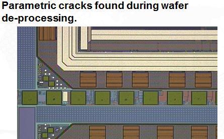
5 Project Objective Evaluate, then release to production a new MEMS vertical probe technology for Al pads Low force probe without sacrificing CCC Contact stability tight planarity and CRES Thermal Agility probe card stability with wide temperature range of -40 o C to 140 o C Minimal pad damage and ILD cracking Production support with field replaceable probes 5

6 Basic Spring Performance Probe Force vs. Over Travel Full Probe cycle of being compressed and released 6 probes measured at once Data after 1.5M cycles 6

7 Basic Spring Performance ISMI Current Carrying Capacity performance of low force vertical spring Data after 1.5M cycles 7
8 Qualification Results

9 Auto Z Performance < 20um planarity Probe card layout x8, 1256 springs, 608 mm 2 array 9


10 Thermal Agility -40 o C 140 o C X, Y and Z optical movement under 10 um across 35 wafers X, Y and Z optical movement under 20 um across 9 wafers Once the card gets to temp, thermal movement is very stable 10

11 Minimal Pad Damage Probing at 80um OT 11

12 AVI Performance (Automated Visual Inspection of Pad Damage) 12


13 Dielectric Cracking & Punch Through 13
14 Max CRES Production Data Much tighter CRES distribution compared to non-mems vertical probe cards 14
15 CRES Over Time 100K TD Life time testing 15

16 Yield Comparison Much tighter yield distribution compared to non-mems vertical probe 16
17 Life Time Data 32 probes measured across array - Very aggressive test Probe Settings: Production wafers in demo mode - 33 TDs per wafer Production cleaning and over travel Number of TD 100,000 Tip Length Loss (um) 2.0 Tip loss for 500k (um) 10.0 Usable Tip Length (um) 19.0 Projected TD Life 950,000 Initial projects of ~1M TD lifetime in production 17
18 Summary Production performance stand out Production performance Planarity Thermal agility over wide temperature range Minimal pad damage, stable AVI and no ILD cracking CRES and Yield Lifetime Compelling new technology to replace existing high volume technologies Flexible MEMS Technology to Reduce Cost of Test for Multi-site Wire Bond Applications 18
19 Acknowledgement Al Wegleitner, Texas Instruments Frank Meza, FormFactor Doug Shuey, FormFactor Kevin Hughes, FormFactor 19
Advance Low Force Probe cards Used on Solder Flip Chip Devices. Daniel Stillman Texas Instruments Kevin Hughes FormFactor
 Advance Low Force Probe cards Used on Solder Flip Chip Devices Daniel Stillman Texas Instruments Kevin Hughes FormFactor Overview Probe Solution Requirements Material Properties and Performance Production
Katana RFx: A New Technology for Testing High Speed RF Applications Within TI
 Katana RFx: A New Technology for Testing High Speed RF Applications Within TI Compan Logo Probe Test Solutions Manager Overview Introduction Objectives Procedures Results Summary Follow-On Work 2 Introduction
Key Considerations to Probe Cu Pillars in High Volume Production
 Key Considerations to Probe Cu Pillars in High Volume Production Alexander Wittig (GLOBALFOUNDRIES) Amy Leong, Tin Nguyen, Tommaso Masi, Jarek Kister, Mike Slessor (Form Factor) Overview Key Industry Trends
Verification of Singulated HBM2 stacks with Die Level Handler. Dave Armstrong Toshiyuki Kiyokawa Quay Nhin
 Verification of Singulated HBM2 stacks with Die Level Handler Dave Armstrong Toshiyuki Kiyokawa Quay Nhin Abstract Background only will delete on final material High-Bandwidth-Memory continues to evolve
Leveraging Multiprobe Probe Card learnings to help Standardize and improve Parametric and WLR Testing
 Leveraging Multiprobe Probe Card learnings to help Standardize and improve Parametric and WLR Testing Company Logo Brandon Mair Dawn Copeland Teas Instruments Agenda Introduction Overview Similarities
A Test-Setup for Probe-Card Characterization
 Contents A test-setup for probe card characterization under Background production-like / Motivation operating conditions Third level 16pt Fourth level 14pt Michael Horn, Stephan Fuchs» Fifth level 12pt
Test and Measurement Challenges for 3D IC Development. R. Robertazzi IBM Research
 Test and Measurement Challenges for 3D IC Development R. Robertazzi IBM Research PFA Bill Price. Pete Sorce. John Ott. David Abraham. Pavan Samudrala Digital Test Kevin Stawaisz. TEL P12 Prober Glen Lansman,
Application Note. Pyramid Probe Cards
 Application Note Pyramid Probe Cards Innovating Test Technologies Pyramid Probe Technology Benefits Design for Test Internal pads, bumps, and arrays High signal integrity Rf and DC on same probe card Small
High Parallelism Memory Test Advances based on MicroSpring Contact Technology
 High Parallelism Memory Test Advances based on MicroSpring Contact Technology Thomas Homorodi- Director of Marketing Robert Martin Technical Sales Eng. Southwest Test Workshop June 2001 Contents Introduction
Rolling Up Solutions of Wafer Probing Technologies Joey Wu
 Rolling Up Solutions of Wafer Probing Technologies Joey Wu Manager, Global Marketing Drivers of Semiconductor Industry Source: Yole, 2016 Source: Yole, 2016 Source: Yole, 2016 Source: Yole, 2016 Form-factor
Low Force MEMS Probe Solution for Full Wafer Single Touch Test
 Matt Losey Yohannes Desta Melvin Khoo Lakshmikanth Namburi Georg Aigeldinger Touchdown Technologies Low Force MEMS Probe Solution for Full Wafer Single Touch Test June 6 to 9, 2010 San Diego, CA USA Towards
3D profiler for contactless probe card inspection. Rob Marcelis
 3D profiler for contactless probe card inspection Rob Marcelis 1 Content Introduction Objectives Challenges Basics DOE Results Data transformation Advantages/disadvantages Summary conclusions Follow up
An Advanced Wafer Probing Characterization Tool for Low CRes at High Current Dr.-Ing. Oliver Nagler Francesco Barbon, Dr.
 An Advanced Wafer Probing Characterization Tool for Low CRes at High Current Dr.-Ing. Francesco Barbon, Dr. Christian Degen Infineon Technologies AG, Germany Dep. of Test Technology & Innovation Overview
High and Low Temperature Wafer Probing Challenges
 High and Low Temperature Wafer Probing Challenges Presenters: Authors: Wei Liang Sio Emanuele Bertarelli Yah Ean Koh Overview Motivation Probing challenges at high/low temperatures Production probing issues
Wafer Probe card solutions
 Wafer Probe card solutions Innovative Solutions to Test Chips in the Semiconductor Industry Our long term experience in the electronic industry and our strong developing and process teams are inspired
Standardizing WSP Wafer Socket Pogo Pin Probe Cards
 John Hite Texas Instruments Standardizing WSP Wafer Socket Pogo Pin Probe Cards June 6 to 9, 2010 San Diego, CA USA Agenda Introduction WLCSP and WSP Probing WSP Standardization Standard Alignment / Mounting
Wafer Probe card solutions
 Wafer Probe card solutions Innovative Solutions to Test Chips in the Semiconductor Industry Our long term experience in the electronic industry and our strong developing and process teams are inspired
PROBE CARD METROLOGY
 PROBE CARD METROLOGY HIGH TEMPERATURE TESTING OF PROBE CARDS Rod Schwartz VP & Technical Director Integrated Technology Corporation Dan Kosecki VP Software Development Integrated Technology Corporation
Panel Discussion Chair: Michael Huebner
 Panel Discussion Chair: Michael Huebner FormFactor Inc. Panel members Panel Discussion Mark Ojeda (Spansion/Cypress) Panel: I/II Rey Rincon (Freescale) Panel: II Al Wegleitner (TI) Panel: I/II Clark Liu
High performance HBM Known Good Stack Testing
 High performance HBM Known Good Stack Testing FormFactor Teradyne Overview High Bandwidth Memory (HBM) Market and Technology Probing challenges Probe solution Power distribution challenges PDN design Simulation
Analysis of probe C.C.C. according to temperature and evaluation method Sanghun Shin, Seongyeon Wi, Yonggeon Shin, Wonha Jeon
 Analysis of probe C.C.C. according to temperature and evaluation method Sanghun Shin, Seongyeon Wi, Yonggeon Shin, Wonha Jeon Willtechnology Co., Ltd. Overview Background Evaluation method Evaluation results
Products, Services & Capabilities
 Products, Services & Capabilities Toll Free: (800) 404-0204 U.S. Only Tel: (952) 229-8200 Fax: (952) 229-8201 email: info@ironwoodelectronics.com Overview Company Overview Founded 1986 Over 5,000 products
Challenges of Integration of Complex FHE Systems. Nancy Stoffel GE Global Research
 Challenges of Integration of Complex FHE Systems Nancy Stoffel GE Global Research Products drive requirements to sub-systems, components and electronics GE PRODUCTS CTQs: SWaP, $$, operating environment,
A Fine Pitch MEMS Probe Card with Built in Active Device for 3D IC Test
 3000.0 2500.0 2000.0 1500.0 1000.0 500.0 0.00-500.0-1000.0-1500.0 OSCILLOSCOPE Design file: MSFT DIFF CLOCK WITH TERMINATORREV2.FFS Designer: Microsoft HyperLynx V8.0 Comment: 650MHz at clk input, J10,
There is a paradigm shift in semiconductor industry towards 2.5D and 3D integration of heterogeneous parts to build complex systems.
 Direct Connection and Testing of TSV and Microbump Devices using NanoPierce Contactor for 3D-IC Integration There is a paradigm shift in semiconductor industry towards 2.5D and 3D integration of heterogeneous
Direct Attach ViProbe Series Probe Cards for Wafer Test
 Direct Attach ViProbe Series Probe Cards for Wafer Test Probe Cards Direct Attach ViProbe Series FEINMETALL Direct Attach ViProbe Series represents a technology in advanced wafer probing. Our Direct Attach
Novel Precision Probe Array for Wafer Level Final Test of WLCSP Jathan Edwards
 Novel Precision Probe Array for Wafer Level Final Test of WLCSP Johnstech International Presentation Outline Introduction to IQtouch Micro Final Test Probe Arrays for 300 500 micron pitch WLCSP Compare/contrast
EE434 ASIC & Digital Systems Testing
 EE434 ASIC & Digital Systems Testing Spring 2015 Dae Hyun Kim daehyun@eecs.wsu.edu 1 Introduction VLSI realization process Verification and test Ideal and real tests Costs of testing Roles of testing A
Production Parametric Test - Challenges and Surprising Outcomes Running in a High Volume Manufacturing Environment
 Production Parametric Test - Challenges and Surprising Outcomes Running in a High Volume Manufacturing Environment Karen Armendariz, Celadon Systems John Reynolds, Freescale Semiconductor Greg Tyrpak,
Using MLOs to Build Vertical Technology Space Transformers
 Presentation to Southwest Test Workshop 2002 Using MLOs to Build Vertical Technology Space Transformers Bill Fulton and Bill Pardee Wentworth Laboratories Overview 1. Terminology 2. Benefits of MLOs vs
Krzysztof Dabrowiecki, Probe2000 Inc Southwest Test Conference, San Diego, CA June 08, 2004
 Structural stability of shelf probe cards Krzysztof Dabrowiecki, Probe2000 Inc Southwest Test Conference, San Diego, CA June 08, 2004 Presentation Outline Introduction Objectives Multi die applications
Socket Technologies
 Socket Technologies Toll Free: (800) 404-0204 U.S. Only Tel: (952) 229-8200 Fax: (952) 229-8201 email: info@ironwoodelectronics.com Introduction Company Overview Over 5,000 products High Performance Adapters
Wafer Level Burn-In and Test System Considerations
 Wafer Level Burn-In and Test System Considerations Mark C. Carbone Program Manager Aehr Test Systems 1667 Plymouth Street Mountain View, CA www.aehr.com Objectives of WLBT Production Burn-in of full wafer
Probing solutions and inherent customization to enable advanced copper-based 3D integration schemes
 Probing solutions and inherent customization to enable advanced copperbased 3D integration schemes Dongpill Yang, SEC Jungwoo Sung, SEC, Technoprobe Raffaele Vallauri, Technoprobe DongHun Lee, Technoprobe
ARCHIVE Multi Level Stacked Socket - Challenges & Solutions Mike Fedde, Ranjit Patil, Ila Pal, Vinayak Panavala Ironwood Electronics
 ARCHIVE 2010 TECHNIQUES, COMPONENTS & ADVANCES FOR NEXT GENERATION TEST Next Generation CiS (Capacitor in Socket) Featuring Discrete Capacitors and Elastomer Hybrid Schemes Shaul Lupo, Omer Vikinski Intel
TSV Test. Marc Loranger Director of Test Technologies Nov 11 th 2009, Seoul Korea
 TSV Test Marc Loranger Director of Test Technologies Nov 11 th 2009, Seoul Korea # Agenda TSV Test Issues Reliability and Burn-in High Frequency Test at Probe (HFTAP) TSV Probing Issues DFT Opportunities
Introduction to Wafer Level Burn-In. William R. Mann General Chairman Southwest Test Workshop
 Introduction to Wafer Level Burn-In William R. Mann General Chairman Southwest Test Workshop Outline Conventional Burn In and Problems Wafer Level BI Driving Factors Initial Die Level BI Technical Challenges
March 4-7, 2018 Hilton Phoenix / Mesa Hotel Mesa, Arizona Archive
 March 4-7, 2018 Hilton Phoenix / Mesa Hotel Mesa, Arizona Archive 2018 BiTS Workshop Image: pilgrims49 / istock COPYRIGHT NOTICE The presentation(s)/poster(s) in this publication comprise the Proceedings
March 6-9, 2016 Hilton Phoenix / Mesa Hotel Mesa, Arizona Archive- Session 5
 Proceedings Archive March 6-9, 2016 Hilton Phoenix / Mesa Hotel Mesa, Arizona Archive- Session 5 2016 BiTS Workshop Image: Stiop / Dollarphotoclub Proceedings Archive Presentation / Copyright Notice The
Probe Card Metrology. Challenges and Solutions. Jim Powell, Applications Engineer Rudolph Technologies
 Probe Card Metrology Challenges and Solutions Jim Powell, Applications Engineer Rudolph Technologies Agenda 1. Overview 2. Cost of Ownership 3. Probe Card Metrology 4. Top Challenges 5. Probe Card Circuit
Impact of DFT Techniques on Wafer Probe
 Impact of DFT Techniques on Wafer Probe Ron Leckie, CEO, INFRASTRUCTURE ron@infras.com Co-author: Charlie McDonald, LogicVision charlie@lvision.com The Embedded Test Company TM Agenda INFRASTRUCTURE Introduction
Autonomous RF Measurement assistant
 Autonomous RF Measurement assistant Gavin Fisher Applications Specialist Customer Application & Product Solutions Why is Device Modeling Critical DEVICE MODELING N+? IC Design IC Fabrication PDK Process
Update: Lambda project
 Update: Lambda project Sabine Lange Detector Group DESY meeting, May 29-31, 2012 s1 Lambda project About Lambda: 2 x 6 3 chips (~28 x 85mm) high frame rate (8 read out lines, 2kHz readout) 10 gigabit Ethernet
300 mm semi-/fully-automated probe system
 300 mm semi-/fully-automated probe system DATA SHEET In device and process development, the right solution helps you handle test requirements that change from day to day. That s why Cascade Microtech developed
Effects of Pad Structure on the Scrub Performance of MEMS Probes for Memory Devices Aaron Woodard
 Effects of Pad Structure on the Scrub Performance of MEMS Probes for Memory Devices Aaron Micron Technology, Inc Outline Background / Trends / Test Requirements Experiment Design Results What Ifs Summary
The Influences of Signal Matching During Multi-site Testing
 Eddie McClanahan and Al Wegleitner Texas Instruments The Influences of Signal Matching During Multi-site Testing 2007 San Diego, CA USA Agenda Background Problem Statement Objective Methodology Results
An integrated solution for KGD: At-speed wafer-level testing and full-contact wafer-level burn-in after flip chip bumping
 An integrated solution for KGD: At-speed wafer-level testing and full-contact wafer-level burn-in after flip chip bumping Yuan-Ping Tseng/ An-Hong Liu TD center ChipMOS Technologies Inc. June 5, 2001 1
Innovative 3D Structures Utilizing Wafer Level Fan-Out Technology
 Innovative 3D Structures Utilizing Wafer Level Fan-Out Technology JinYoung Khim #, Curtis Zwenger *, YoonJoo Khim #, SeWoong Cha #, SeungJae Lee #, JinHan Kim # # Amkor Technology Korea 280-8, 2-ga, Sungsu-dong,
Multi-Die Packaging How Ready Are We?
 Multi-Die Packaging How Ready Are We? Rich Rice ASE Group April 23 rd, 2015 Agenda ASE Brief Integration Drivers Multi-Chip Packaging 2.5D / 3D / SiP / SiM Design / Co-Design Challenges: an OSAT Perspective
SKTM Socket Series Catalog High Speed Compression Mount
 SKTM Socket Series Catalog High Speed Compression Mount Ardent Design Support Sockets Overview Ardent Compliant Contact Technology Socket Types BGA/LGA QFN/QFP/MEMS Optical Plunge to Board Lid Types Ordering
Real Time Contact Resistance Measurement & Control. Tony Schmitz Erwin Barret
 Real Time Contact Resistance Measurement & Control Tony Schmitz Erwin Barret Introduction Agenda Why is CRES control important? Objectives of Real Time Method Offline Method Limitations & Goals of Real
Applications, Processing and Integration Options for High Dielectric Constant Multi-Layer Thin-Film Barium Strontium Titanate (BST) Capacitors
 Capacitors") Applications, Processing and Integration Options for High Dielectric Constant Multi-Layer Thin-Film Barium Strontium Titanate (BST) Capacitors Agenda Introduction What is BST? Unique Characteristics of
Applications, Processing and Integration Options for High Dielectric Constant Multi-Layer Thin-Film Barium Strontium Titanate (BST) Capacitors Agenda Introduction What is BST? Unique Characteristics of
Measuring Z-stage accuracy using a force sensor
 Measuring Z-stage accuracy using a force sensor Sancho Adam Southwest Test Conference June 2007 Contents Introduction / Background Objectives / Goals Methods / Materials / Procedures Results / Relevant
Non-contact Test at Advanced Process Nodes
 Chris Sellathamby, J. Hintzke, B. Moore, S. Slupsky Scanimetrics Inc. Non-contact Test at Advanced Process Nodes June 8-11, 8 2008 San Diego, CA USA Overview Advanced CMOS nodes are a challenge for wafer
High Volume Manufacturing Supply Chain Ecosystem for 2.5D HBM2 ASIC SiPs
 Open-Silicon.com 490 N. McCarthy Blvd, #220 Milpitas, CA 95035 408-240-5700 HQ High Volume Manufacturing Supply Chain Ecosystem for 2.5D HBM2 ASIC SiPs Open-Silicon Asim Salim VP Mfg. Operations 20+ experience
Metrology and Probe Repair challenges with tighter pitch probe cards
 Anil Kaza Intel Corporation Metrology and Probe Repair challenges with tighter pitch probe cards June 6 to 9, 2010 San Diego, CA USA Overview Current trends with technology generation Intel PCM Work Flow
MACHINE VISION FOR SMARTPHONES. Essential machine vision camera requirements to fulfill the needs of our society
 MACHINE VISION FOR SMARTPHONES Essential machine vision camera requirements to fulfill the needs of our society INTRODUCTION With changes in our society, there is an increased demand in stateof-the art
Monday 3/10/14 3:30pm
 Monday 3/10/14 3:30pm DOING THE HEAVY LIFTING Within burn-in and test strategies the heavy lifting that falls to the technologies within test systems is this session's focus. The first paper outlines the
Stacked Silicon Interconnect Technology (SSIT)
") Stacked Silicon Interconnect Technology (SSIT) Suresh Ramalingam Xilinx Inc. MEPTEC, January 12, 2011 Agenda Background and Motivation Stacked Silicon Interconnect Technology Summary Background and Motivation
Stacked Silicon Interconnect Technology (SSIT) Suresh Ramalingam Xilinx Inc. MEPTEC, January 12, 2011 Agenda Background and Motivation Stacked Silicon Interconnect Technology Summary Background and Motivation
Packaging of Selected Advanced Logic in 2x and 1x nodes. 1 I TechInsights
 Packaging of Selected Advanced Logic in 2x and 1x nodes 1 I TechInsights Logic: LOGIC: Packaging of Selected Advanced Devices in 2x and 1x nodes Xilinx-Kintex 7XC 7 XC7K325T TSMC 28 nm HPL HKMG planar
Future Trends One Mann s Opinion
 Future Trends One Mann s Opinion Bill Mann General Chair - SWTW Southwest Test Workshop Newport Beach, CA 92663 949-645-3294 william.mann@ieee.org Future Trends One Mann s Opinion Relative Reduction in
LTCC (Low Temperature Co-fired Ceramic)
") LTCC (Low Temperature Co-fired Ceramic) Design Guide Line. 381, Wonchun-Dong, Paldal-Ku, Suwon City, Kyung Ki-Do, Republic of Korea Tel : 82-31-217-2500 (Ext. 470) Fax : 82-31-217-7316 Homepage : http://www.pilkorcnd.co.kr
LTCC (Low Temperature Co-fired Ceramic) Design Guide Line. 381, Wonchun-Dong, Paldal-Ku, Suwon City, Kyung Ki-Do, Republic of Korea Tel : 82-31-217-2500 (Ext. 470) Fax : 82-31-217-7316 Homepage : http://www.pilkorcnd.co.kr
A Fine Pitch MEMS Probe Card with Built in Ac8ve Device for 3D IC Test
 A Fine Pitch MEMS Probe Card with Built in Ac8ve Device for 3D IC Test Lakshmikanth Namburi Florent Cros Yong Hong Ting Hu Robert Smith ADVANTEST Gary Maier Van Thanh Truong Hsichang Liu Katsuyuki Sakuma
Non-destructive, High-resolution Fault Imaging for Package Failure Analysis. with 3D X-ray Microscopy. Application Note
 Non-destructive, High-resolution Fault Imaging for Package Failure Analysis with 3D X-ray Microscopy Application Note Non-destructive, High-resolution Fault Imaging for Package Failure Analysis with 3D
Additional Slides for Lecture 17. EE 271 Lecture 17
 Additional Slides for Lecture 17 Advantages/Disadvantages of Wire Bonding Pros Cost: cheapest packages use wire bonding Allows ready access to front side of die for probing Cons Relatively high inductance
High Reliability Electronics for Harsh Environments
 High Reliability Electronics for Harsh Environments Core Capabilities API Technologies is a world leader in the supply of microelectronic products and services supporting mission critical applications,
MPI TS150-HP 150 mm High Power Manual Probe System For accurate High Power measurements up to 10 kv, 600 A
 MPI TS15-HP 15 mm High Power Manual Probe System For accurate High Power measurements up to 1 kv, 6 A FEATURES / BENEFITS Universal Use Designed specifically for high power device measurement and wide
Gavin Fisher Cascade Microtech Europe
 Gavin Fisher Cascade Microtech Europe Device measurement at it s simplest requires the following steps Probe and accessory physical Set-up for calibration Calibration instrumentation setting preparation
About the Instructor
 About the Instructor Kwang-Ting (Tim) Cheng PhD, 1988, Univ. of California, Berkeley 1988-1993: AT&T Bell Labs 1993-Present: Professor, Dept. of ECE, Univ. of California, Santa Barbara 1999-2002: Director,
Globalization and its Impact on the Probing Process. Alan Romriell (Spansion) Manish Gulati (FormFactor)
 Manish Gulati (FormFactor)") Globalization and its Impact on the Probing Process Alan Romriell (Spansion) Manish Gulati (FormFactor) Recent article in EE Times Top 20 risk factors for tech companies Junko Yoshida (05/19/2008 3:52
Globalization and its Impact on the Probing Process Alan Romriell (Spansion) Manish Gulati (FormFactor) Recent article in EE Times Top 20 risk factors for tech companies Junko Yoshida (05/19/2008 3:52
BiTS Poster Session. March 5-8, Hilton Phoenix / Mesa Hotel Mesa, Arizona. Archive Poster BiTS Workshop Image: tonda / istock
 March 5-8, 2017 Hilton Phoenix / Mesa Hotel Mesa, Arizona Archive Poster 2017 BiTS Workshop Image: tonda / istock Copyright Notice The presentation(s)/poster(s) in this publication comprise the Proceedings
Total Inspection Solutions Ensuring Known-Good 3DIC Package. Nevo Laron, Camtek USA, Santa Clara, CA
 Total Inspection Solutions Ensuring Known-Good 3DIC Package Nevo Laron, Camtek USA, Santa Clara, CA Density Packaging Trends vs. Defect Costs Functionality Package Yield 3DIC yield statistics 101 1.00
Wafer Level Packaging The Promise Evolves Dr. Thomas Di Stefano Centipede Systems, Inc. IWLPC 2008
 Wafer Level Packaging The Promise Evolves Dr. Thomas Di Stefano Centipede Systems, Inc. IWLPC 2008 / DEVICE 1.E+03 1.E+02 1.E+01 1.E+00 1.E-01 1.E-02 1.E-03 1.E-04 1.E-05 1.E-06 1.E-07 Productivity Gains
ENG04057 Teste de Sistema Integrados. Prof. Eric Ericson Fabris (Marcelo Lubaszewski)
") ENG04057 Teste de Sistema Integrados Prof. Eric Ericson Fabris (Marcelo Lubaszewski) Março 2011 Slides adapted from ABRAMOVICI, M.; BREUER, M.; FRIEDMAN, A. Digital Systems Testing and Testable Design.
ENG04057 Teste de Sistema Integrados Prof. Eric Ericson Fabris (Marcelo Lubaszewski) Março 2011 Slides adapted from ABRAMOVICI, M.; BREUER, M.; FRIEDMAN, A. Digital Systems Testing and Testable Design.
WHICH SIDE ARE YOU ON? DOUBLE SIDED PROBING
 WHICH SIDE ARE YOU ON? DOUBLE SIDED PROBING Traditionally, devices with active regions on both sides of a wafer were limited to discrete devices. With advances in materials, functionality and packaging,
56/80 Gb/s PCB transmission lines. and. 56 Gb/s End-launch GPPO connector
 White paper: WP141-1 56/8 b/s PCB transmission lines and 56 b/s End-launch PPO connector ----- Electrical Interconnection basic technology development ----- Takada RF Labs, Inc. 214/1/2 E-mail: contact@takadarf.com
An Introduction To Area Array Probing
 An Introduction To Area Array Probing Fred Taber IBM Corporation 1998 Southwest Test WorkShop 1 Topics: Introduction & Background Considerations & Experiences Q & A 2 Introduction & Background Vertical
Thin n-in-p planar pixel modules for the ATLAS upgrade at HL-LHC
 Thin n-in-p planar pixel modules for the ATLAS upgrade at HL-LHC A. Macchiolo, J. Beyer, A. La Rosa, R. Nisius, N. Savic Max-Planck-Institut für Physik, Munich 8 th International Workshop on Semiconductor
Advances in Probe Card Analyzers
 Providing Leading Edge Technology to Meet Your Future Requirements Advances in Probe Card Analyzers Test and Maintenance of Very High Pin Count Cards Rod Schwartz VP & Technical Director Integrated Technology
Photonics Integration in Si P Platform May 27 th Fiber to the Chip
 Photonics Integration in Si P Platform May 27 th 2014 Fiber to the Chip Overview Introduction & Goal of Silicon Photonics Silicon Photonics Technology Wafer Level Optical Test Integration with Electronics
2D nano PrintArray Product Data Sheet
 NSCRIPTOR Product Data Sheet Dip Pen Nanolithography (DPN ) is the process of writing nanoscale patterns of molecular "ink" onto a sample substrate via a coated SPM tip. NanoInk s NSCRIPTOR DPN System
DesignCon 2005 Track 5: Chip and Board Interconnect Design (5-TA2)
") DesignCon 2005 Track 5: Chip and Board Interconnect Design (5-TA2) Connector-Less Probing: Electrical and Mechanical Advantages Authors/Presenters: Brock LaMeres, Agilent Technologies Brent Holcombe, Agilent
DesignCon 2005 Track 5: Chip and Board Interconnect Design (5-TA2) Connector-Less Probing: Electrical and Mechanical Advantages Authors/Presenters: Brock LaMeres, Agilent Technologies Brent Holcombe, Agilent
Advanced Packaging For Mobile and Growth Products
 Advanced Packaging For Mobile and Growth Products Steve Anderson, Senior Director Product and Technology Marketing, STATS ChipPAC Growing Needs for Silicon & Package Integration Packaging Trend Implication
Packaging for parallel optical interconnects with on-chip optical access
 Packaging for parallel optical interconnects with on-chip optical access I. INTRODUCTION Parallel optical interconnects requires the integration of lasers and detectors directly on the CMOS chip. In the
Motorola Wafer Level Burn-in and Test
 Motorola Wafer Level Burn-in and Test 00 Southwest Test Workshop Teresa McKenzie, Wafer Level Burn In Engineer Motorola (T.McKenzie@motorola.com) 6501 William Cannon Drive West; Austin, Texas 78735; 51-895-486
12500 TI Boulevard, MS 8640, Dallas, Texas 75243
 2500 TI Boulevard, MS 8640, Dallas, Texas 75243 PN 2060309000 TPS6223TDRYRQ and TPS62234TDRYRQ LLGA to etch and Datasheet update for TPS6223-Q/TPS62234-Q Final hange Notification Date: 3/30/206 To: EBV
Known-Good-Die (KGD) Wafer-Level Packaging (WLP) Inspection Tutorial
 Wafer-Level Packaging (WLP) Inspection Tutorial") Known-Good-Die (KGD) Wafer-Level Packaging (WLP) Inspection Tutorial Approach to Inspection Wafer inspection process starts with detecting defects and ends with making a decision on what to do with both
Known-Good-Die (KGD) Wafer-Level Packaging (WLP) Inspection Tutorial Approach to Inspection Wafer inspection process starts with detecting defects and ends with making a decision on what to do with both
Use of Resource Sharing Techniques to Increase Parallel Test and Test Coverage in Wafer Test Michael Huebner
 Use of Resource Sharing Techniques to Increase Parallel Test and Test Coverage in Wafer Test Michael Huebner FormFactor, Inc Mo>va>on With increasing test >mes/dut and die per wafer, test >me/wafer and
BGA Socketing Systems
 DATA BOOK BGA-TECH04 (REV. 3/04) BGA Socketing Systems Search for a footprint or build a part number online at www.bgasockets.com Solutions for Virtually Any BGA Application BGA Socket Adapter System Designed
Improvement of ELK Reliability in Flip Chip Packages using Bond-on-Lead (BOL) Interconnect Structure
 Interconnect Structure") Improvement of ELK Reliability in Flip Chip Packages using Bond-on-Lead (BOL) Interconnect Structure by Eric Ouyang, MyoungSu Chae, Seng Guan Chow, Roger Emigh, Mukul Joshi, Rob Martin, Raj Pendse STATS
Improvement of ELK Reliability in Flip Chip Packages using Bond-on-Lead (BOL) Interconnect Structure by Eric Ouyang, MyoungSu Chae, Seng Guan Chow, Roger Emigh, Mukul Joshi, Rob Martin, Raj Pendse STATS
Testing Principle Verification Testing
 ECE 553: TESTING AND TESTABLE DESIGN OF DIGITAL SYSTES Test Process and Test Equipment Overview Objective Types of testing Verification testing Characterization testing Manufacturing testing Acceptance
SFC ChipClamp ΤΜ Flip Chip TVS Diode with T-Filter PRELIMINARY Features
 Description The SFC2282-50 is a low pass T-filter with integrated TVS diodes. It is designed to provide bidirectional filtering of EMI/RFI signals and electrostatic discharge (ESD) protection in portable
Extra Large Multi-DUT Array Probing enabling > X100 Parallel Testing
 Extra Large Multi-DUT Array Probing enabling > X100 Parallel Testing Bassam Dabit FAB18 Test Process Integration Trung Nguyen CTM Test Process Integration Intel Corporation 06/06/2005 Introduction Motivation
Vertical Circuits. Small Footprint Stacked Die Package and HVM Supply Chain Readiness. November 10, Marc Robinson Vertical Circuits, Inc
 Small Footprint Stacked Die Package and HVM Supply Chain Readiness Marc Robinson Vertical Circuits, Inc November 10, 2011 Vertical Circuits Building Blocks for 3D Interconnects Infrastructure Readiness
Test Cell Co-planarity Optimization Presenter: Troy Harnisch
 Test Cell Co-planarity Optimization Presenter: Troy Harnisch Teradyne Co-authors: Doug Garrett, NXP Hoang Nguyen, Microsemi What is co-planarity of a test cell Parallel plane between wafer chuck and probe
MPI TS150-THZ 150 mm Manual Probe System
 MPI TS150-THZ 150 mm Manual Probe System Industry s first explicitly designed probe system for accurate measurements at mm-wave and sub-mm wave (THz) frequency range FEATURES / BENEFITS Variety of Applications
Session 4a. Burn-in & Test Socket Workshop Burn-in Board Design
 Session 4a Burn-in & Test Socket Workshop 2000 Burn-in Board Design BURN-IN & TEST SOCKET WORKSHOP COPYRIGHT NOTICE The papers in this publication comprise the proceedings of the 2000 BiTS Workshop. They
Bringing 3D Integration to Packaging Mainstream
 Bringing 3D Integration to Packaging Mainstream Enabling a Microelectronic World MEPTEC Nov 2012 Choon Lee Technology HQ, Amkor Highlighted TSV in Packaging TSMC reveals plan for 3DIC design based on silicon
Advanced Wafer Level Chip Scale Packaging Solution for Industrial CMOS Image Sensors Jérôme Vanrumbeke
 Advanced Wafer Level Chip Scale Packaging Solution for Industrial CMOS Image Sensors Jérôme Vanrumbeke Project Manager, Professional Imaging Agenda Agenda e2v Professional Imaging WLCSP for CIS Background
MPI TS150-AIT 150 mm Manual Probe System
 MPI TS150-AIT 150 mm Manual Probe System Industry s first explicitly designed 150 mm probe system providing accurate tests for mm-wave, THz, and automated impedance tuner applications FEATURES / BENEFITS