Wafer Probe card solutions
|
|
|
- Lee Berniece Floyd
- 6 years ago
- Views:
Transcription

1


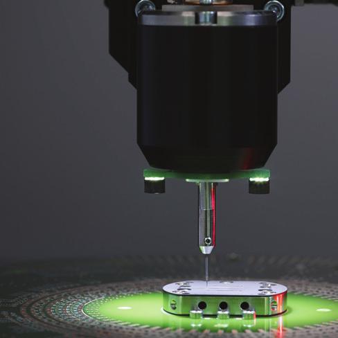
2 Wafer Probe card solutions Innovative Solutions to Test Chips in the Semiconductor Industry Our long term experience in the electronic industry and our strong developing and process teams are inspired to create the future and to support the semiconductor industry. It is our passion to satisfy your demand as our customers with a comprehensive variety of solutions. ViProbe Vertical probe card with buckling beams for contacting on aluminum, copper, gold, palladium and other pads. Page 4 MµProbe / LiProbe Contacting solutions for pads and copper pillars using solid and lamella MEMS beams. Page 5 FeinProbe Probe card with spring contact probes for WLCSP, SiP, analog and mixed signal flip chip applications. Page 6 CiProbe Probe card with cobra like beams for testing of analog and mixed signal, flip chip and grid array solder bump applications. Page 7 Cantilever Probe Cards Probe card with epoxy ring and needles for a wide range of applications. Page 7 2


3 Wafer Probe card Competence Micro-mechanical Processes Manufacturing probe cards for wafer testing is based on handling finest structures and micro-mechanical processes. Our world is to place thousands of contact elements in the size of a human hair exactly on a tiny space in the size of a post stamp. And our manufacturing equipment is optimized for these requirements of the semiconductor industry. We Make the Impossible Possible Innovative technologies meet the extremely high demands of precision and quality for manufacturing our products. Clean rooms and manufacturing facilities, test equipment and specially developed machines combined with consequent and continual process optimization lead to low error rates, short lead times and a high process stability. Core Competence Micro Hole Drilling Finest drillings and highest precision of their position allow an exact placement of the contact elements in a probe card head. The basic material for heads is ceramics, the minimum diameter of drill holes depends on the drilling technology. Mechanical drilling allows diameters down to 40 µm whereas laser drilling even results in diameters down to 30 µm. Outstanding Test Equipment State of the art probe card analyzers guarantee a final inspection of each probe card. A wide variety of testers allow a maximum of test flexibility and reliability. Flying probe testers enable inspections of SMD components on PCBs. Special test equipment has been implemented as inspection gates for high product quality and early failure detection along manufacturing. Flexibility by In-house SMD Assembly Automatic SMD assembly and semiautomatic connector wiring lead to a high degree of flexibility and quality of the electrical performance of a probe card. A jet printer applies solder paste on PCBs up to a size of 500 mm x 600 mm without soldering mask and a placement machine handles even smallest components. 3


4 Vertical Probe Card ViProbe FEINMETALL ViProbe is the buckling beam technology for contacting pads. The contact can be done with and without scrub - depending on the application. It perfectly fits for contacting on aluminum, copper, gold, palladium and other pad materials. Excellent temperature behavior Easy maintenance & service Easy exchange of beams Precise alignment over the entire lifetime Robustness Application Examples ViProbe - SOC Wired connector Head size: 45 mm x 45 mm Pin count: Beam size: 2.5 mil Number of DUTs: 24 Tester: Teradyne J750 ViProbe - Multi DUT MCU MLC Space transformer connector Head size: 40 mm x 40 mm Pin count: Beam size: 1.6 mil Number of DUTs: 32 Tester: Advantest V93000 ViProbe - High Multi DUT Digital Direct Attach connector Head size: 80 mm x 80 mm Pin count: Beam size: 2 mil Number of DUTs: Tester: Advantest J996 Specifications at a glance Contact elements 3 mil mil - 2 mil mil Pitch down to 56 µm Pin count more than Active area up to 100 mm x 100 mm Temperature range -55 C to 180 C 4 Subject to change without notice. Further information at


5 MEMS Probe Cards MµProbe and LiProbe FEINMETALL MEMS probe cards are using latest production processes to obtain the solid and lamella MEMS beams used for contacting even smallest pitches in high-current applications. Compatibility with our well-established probe card setup is thereby guaranteed and ensures a reliable functionality. It is the optimal addition to our product range, especially developed to contact small pitch copper pillars and aluminum pads. Long lifetime due to shimming High density Short beams possible with low force High current in respect to density and pitch Patented lamella design beam Application Examples LiProbe - SOC Hybrid space transformer connector Head size: 30 mm x 30 mm Pin count: Number of DUTs: 9 Tester: Teradyne UltraFlex MµProbe - GPU MLC space transformer connector Head size: 40 mm x 40 mm Pin count: Number of DUTs: 4 Tester: Teradyne J750 Specifications at a glance Contact elements M, N for copper pillars and R, L for pads Pitch 80 µm array for copper pillars and 50 µm for pads Pin count more than Active area up to 100 mm x 100 mm Temperature range - 55 C to 200 C Subject to change without notice. Further information at 5


6 Probe Card FeinProbe FEINMETALL FeinProbe is based on spring contact probes as contact elements. This technology is ideal for fine pitches of WLP applications and can be used for WLCSP, WLAN, RF, SiP, analog and mixed signal flip chip applications. Stable and consistent contact resistance with low bump damage High bandwidth of contact elements (up to 10 GHz and higher) Best for high current applications (up to 2,1 A) Suitable for test of single or multi packages together with manual actuators Low risk of damaging bumps Application Examples FeinProbe X01 - WLCSP Direct Attach connector Head size: 20 mm x 20 mm Pin count: Tester: Teradyne UltraFlex FeinProbe X02 - Sensor Direct Attach connector Head size: 32 mm x 32 mm Pin count: 500 Tester: Teradyne J750 Specifications at a glance Contact elements X01, X02, X03, X04 Pitch down to 250 µm Pin count up to Active area up to 60 mm x 60 mm Temperature range -40 C to 150 C 6 Subject to change without notice. Further information at


7 Probe Card CiProbe FEINMETALL CiProbe is based on preformed wire contact elements. It is ideal for testing CPU or GPU processors, FPGA, analog and mixed signal, flip chip and grid array solder bump applications. Best for contacting on lead free solder bumps Best for high current applications (up to 3 A) Mature and robust technology Application Example CiProbe - CSBGA Substrate connector Pin count: 600 Beam size: 4 mil Tester: Catalyst Cantilever Probe Cards FEINMETALL Cantilever probe cards are based on the approved epoxy ring design. The technology is suitable for pads as well as for bumps. Different needle materials, diameters and tip diameters cover a wide range of applications. Fast lead time High current applications Dual temperature possible - wide temperature range Application Example Single DUT - SOC Needle diameter: 4 mil Needle pitch: 100 μm Tester: MT 256 Specifications at a glance CiProbe Cantilever Probe Cards Contact elements: 5 mil - 4 mil - 3 mil 4 mil - 12 mil (customized) Pitch: down to 150 µm area array down to 65 µm Pin count: up to up to Active Area up to 60 mm x 60 mm - Temperature range: -40 C to 150 c -40 C to 180 C Subject to change without notice. Further information at 7
 408 432 7500 info.us@feinmetall.")
 3 560 15 66 info@tw.feinmetall.")
8 International Wafer Probe card contacts FEINMETALL GMBH Herrenberg, Germany (+49) FEINMETALL USA LLC San Jose, USA (+1) FEINMETALL Singapore Pte Ltd SINGAPORE (+65) FEINMETALL-OCT Hsinchu County, TAIWAN (+886) info@tw.feinmetall.com Version 2
Wafer Probe card solutions
 Wafer Probe card solutions Innovative Solutions to Test Chips in the Semiconductor Industry Our long term experience in the electronic industry and our strong developing and process teams are inspired
Direct Attach ViProbe Series Probe Cards for Wafer Test
 Direct Attach ViProbe Series Probe Cards for Wafer Test Probe Cards Direct Attach ViProbe Series FEINMETALL Direct Attach ViProbe Series represents a technology in advanced wafer probing. Our Direct Attach
Application Note. Pyramid Probe Cards
 Application Note Pyramid Probe Cards Innovating Test Technologies Pyramid Probe Technology Benefits Design for Test Internal pads, bumps, and arrays High signal integrity Rf and DC on same probe card Small
Rolling Up Solutions of Wafer Probing Technologies Joey Wu
 Rolling Up Solutions of Wafer Probing Technologies Joey Wu Manager, Global Marketing Drivers of Semiconductor Industry Source: Yole, 2016 Source: Yole, 2016 Source: Yole, 2016 Source: Yole, 2016 Form-factor
Products, Services & Capabilities
 Products, Services & Capabilities Toll Free: (800) 404-0204 U.S. Only Tel: (952) 229-8200 Fax: (952) 229-8201 email: info@ironwoodelectronics.com Overview Company Overview Founded 1986 Over 5,000 products
Advanced CSP & Turnkey Solutions. Fumio Ohyama Tera Probe, Inc.
 Advanced CSP & Turnkey Solutions Fumio Ohyama Tera Probe, Inc. Tera Probe - Corporate Overview 1. Company : Tera Probe, Inc. 2. Founded : August, 2005 3. Capital : Approx. USD118.2 million (as of March
PROBE CARD METROLOGY
 PROBE CARD METROLOGY HIGH TEMPERATURE TESTING OF PROBE CARDS Rod Schwartz VP & Technical Director Integrated Technology Corporation Dan Kosecki VP Software Development Integrated Technology Corporation
Review of New, Flexible MEMS Technology to Reduce Cost of Test for Multi-site Wire Bond Applications
 Review of New, Flexible MEMS Technology to Reduce Cost of Test for Multi-site Wire Bond Applications Dan Stillman Texas Instruments Ben Eldridge FormFactor Overview Project Background & Objective Probe
Package (1C) Young Won Lim 3/20/13
 Young Won Lim 3/20/13") Copyright (c) 2011-2013 Young W. Lim. Permission is granted to copy, distribute and/or modify this document under the terms of the GNU Free Documentation License, Version 1.2 or any later version published
Copyright (c) 2011-2013 Young W. Lim. Permission is granted to copy, distribute and/or modify this document under the terms of the GNU Free Documentation License, Version 1.2 or any later version published
Socket Technologies
 Socket Technologies Toll Free: (800) 404-0204 U.S. Only Tel: (952) 229-8200 Fax: (952) 229-8201 email: info@ironwoodelectronics.com Introduction Company Overview Over 5,000 products High Performance Adapters
Package (1C) Young Won Lim 3/13/13
 Young Won Lim 3/13/13") Copyright (c) 2011-2013 Young W. Lim. Permission is granted to copy, distribute and/or modify this document under the terms of the GNU Free Documentation License, Version 1.2 or any later version published
Copyright (c) 2011-2013 Young W. Lim. Permission is granted to copy, distribute and/or modify this document under the terms of the GNU Free Documentation License, Version 1.2 or any later version published
Key Considerations to Probe Cu Pillars in High Volume Production
 Key Considerations to Probe Cu Pillars in High Volume Production Alexander Wittig (GLOBALFOUNDRIES) Amy Leong, Tin Nguyen, Tommaso Masi, Jarek Kister, Mike Slessor (Form Factor) Overview Key Industry Trends
Over 5,000 products High Performance Adapters and Sockets Many Custom Designs Engineering Electrical and Mechanical ISO9001:2008 Registration
 Overview Company Overview Over 5,000 products High Performance Adapters and Sockets Many Custom Designs Engineering Electrical and Mechanical ISO9001:2008 Registration Adapter Technology Overview Pluggable
#redcube. REDCUBE PRESS-FIT REDCUBE PLUG REDCUBE SMD REDCUBE THR
 #redcube REDCUBE Terminals are the most reliable high-power contacts on PCB level. Low contact resistance guarantees minimum self-heating. Four different designs cover all leading processing technologies
Company Overview March 12, Company Overview. Tuesday, October 03, 2017
 Company Overview Tuesday, October 03, 2017 HISTORY 1987 2001 2008 2016 Company started to design and manufacture low-cost, highperformance IC packages. Focus on using advanced organic substrates to reduce
High performance HBM Known Good Stack Testing
 High performance HBM Known Good Stack Testing FormFactor Teradyne Overview High Bandwidth Memory (HBM) Market and Technology Probing challenges Probe solution Power distribution challenges PDN design Simulation
Verification of Singulated HBM2 stacks with Die Level Handler. Dave Armstrong Toshiyuki Kiyokawa Quay Nhin
 Verification of Singulated HBM2 stacks with Die Level Handler Dave Armstrong Toshiyuki Kiyokawa Quay Nhin Abstract Background only will delete on final material High-Bandwidth-Memory continues to evolve
Adapter Technologies
 Adapter Technologies Toll Free: (800) 404-0204 U.S. Only Tel: (952) 229-8200 Fax: (952) 229-8201 email: info@ironwoodelectronics.com Introduction Company Overview Over 5,000 products High Performance Adapters
Advance Low Force Probe cards Used on Solder Flip Chip Devices. Daniel Stillman Texas Instruments Kevin Hughes FormFactor
 Advance Low Force Probe cards Used on Solder Flip Chip Devices Daniel Stillman Texas Instruments Kevin Hughes FormFactor Overview Probe Solution Requirements Material Properties and Performance Production
Burn-in & Test Socket Workshop
 Burn-in & Test Socket Workshop IEEE March 4-7, 2001 Hilton Mesa Pavilion Hotel Mesa, Arizona IEEE COMPUTER SOCIETY Sponsored By The IEEE Computer Society Test Technology Technical Council COPYRIGHT NOTICE
Using MLOs to Build Vertical Technology Space Transformers
 Presentation to Southwest Test Workshop 2002 Using MLOs to Build Vertical Technology Space Transformers Bill Fulton and Bill Pardee Wentworth Laboratories Overview 1. Terminology 2. Benefits of MLOs vs
Functional Testing of 0.3mm pitch Wafer Level Packages to Multi- GHz Speed made possible by Innovative Socket Technology
 Functional Testing of 0.3mm pitch Wafer Level Packages to Multi- GHz Speed made possible by Innovative Socket Technology Ila Pal - Ironwood Electronics Introduction Today s electronic packages have high
MPI TS2500-RF 200 mm Fully Automated Probe System For RF Production Test Measurements
 MPI TS2500-RF 200 mm Fully Automated Probe System For RF Production Test Measurements FEATURES / BENEFITS Designed for Wide Variety of RF On-Wafer Production Applications RF applications up to 67 GHz &
Socket Technologies
 Socket Technologies Introduction Company Overview Over 5,000 products High Performance Adapters and Sockets Many Custom Designs Engineering Electrical and Mechanical ISO9001:2008 Registration Socket Technology
Standardizing WSP Wafer Socket Pogo Pin Probe Cards
 John Hite Texas Instruments Standardizing WSP Wafer Socket Pogo Pin Probe Cards June 6 to 9, 2010 San Diego, CA USA Agenda Introduction WLCSP and WSP Probing WSP Standardization Standard Alignment / Mounting
Low Force MEMS Probe Solution for Full Wafer Single Touch Test
 Matt Losey Yohannes Desta Melvin Khoo Lakshmikanth Namburi Georg Aigeldinger Touchdown Technologies Low Force MEMS Probe Solution for Full Wafer Single Touch Test June 6 to 9, 2010 San Diego, CA USA Towards
Wafer Level Packaging The Promise Evolves Dr. Thomas Di Stefano Centipede Systems, Inc. IWLPC 2008
 Wafer Level Packaging The Promise Evolves Dr. Thomas Di Stefano Centipede Systems, Inc. IWLPC 2008 / DEVICE 1.E+03 1.E+02 1.E+01 1.E+00 1.E-01 1.E-02 1.E-03 1.E-04 1.E-05 1.E-06 1.E-07 Productivity Gains
Socket Mounting Recommendations and Reflow Profile
 Purpose This document is meant to serve as a guide for mounting E-tec surface mount device (SMD) sockets to the printed circuit board (PCB). The recommendations described here are guidelines only, and
SKTM Socket Series Catalog High Speed Compression Mount
 SKTM Socket Series Catalog High Speed Compression Mount Ardent Design Support Sockets Overview Ardent Compliant Contact Technology Socket Types BGA/LGA QFN/QFP/MEMS Optical Plunge to Board Lid Types Ordering
S e l e c t i v e S o l d e r i n g S y s t e m S E H O S E L E C TL I N E - C. Total Solutions. SEHO SelectLine-C
 Total Solutions for Soldering Processes and Automated Production Lines SEHO SelectLine-C S e l e c t i v e S o l d e r i n g S y s t e m S E H O S E L E C TL I N E - C Patented by SEHO: Ultrasonic Cleaning
Challenges of Integration of Complex FHE Systems. Nancy Stoffel GE Global Research
 Challenges of Integration of Complex FHE Systems Nancy Stoffel GE Global Research Products drive requirements to sub-systems, components and electronics GE PRODUCTS CTQs: SWaP, $$, operating environment,
Packaging Technology for Image-Processing LSI
 Packaging Technology for Image-Processing LSI Yoshiyuki Yoneda Kouichi Nakamura The main function of a semiconductor package is to reliably transmit electric signals from minute electrode pads formed on
High and Low Temperature Wafer Probing Challenges
 High and Low Temperature Wafer Probing Challenges Presenters: Authors: Wei Liang Sio Emanuele Bertarelli Yah Ean Koh Overview Motivation Probing challenges at high/low temperatures Production probing issues
Embedded Power Dies for System-in-Package (SiP)
") Embedded Power Dies for System-in-Package (SiP) D. Manessis, L. Boettcher, S. Karaszkiewicz, R.Patzelt, D. Schuetze, A. Podlasky, A. Ostmann Fraunhofer Institute for Reliability and Microintegration (IZM),
Embedded Power Dies for System-in-Package (SiP) D. Manessis, L. Boettcher, S. Karaszkiewicz, R.Patzelt, D. Schuetze, A. Podlasky, A. Ostmann Fraunhofer Institute for Reliability and Microintegration (IZM),
Vertical Circuits. Small Footprint Stacked Die Package and HVM Supply Chain Readiness. November 10, Marc Robinson Vertical Circuits, Inc
 Small Footprint Stacked Die Package and HVM Supply Chain Readiness Marc Robinson Vertical Circuits, Inc November 10, 2011 Vertical Circuits Building Blocks for 3D Interconnects Infrastructure Readiness
Wafer Level Packaging & Bumping A view from a European Service Provider
 9 th International IEEE CPMT Symposium on High Density Design, Packaging and Microsystem Integration (HDP 07) 26 th -28 th June 2007 Shanghai, China Wafer Level Packaging & Bumping A view from a European
Area Array Probe Card Interposer. Raphael Robertazzi IBM Research 6/4/01. 6/4/01 IBM RESEARCH Page [1]
![Area Array Probe Card Interposer. Raphael Robertazzi IBM Research 6/4/01. 6/4/01 IBM RESEARCH Page [1]](/thumbs/78/78371092.jpg "Area Array Probe Card Interposer. Raphael Robertazzi IBM Research 6/4/01. 6/4/01 IBM RESEARCH Page [1]") Area Array Probe Card Interposer Raphael Robertazzi IBM Research 6/4/01 6/4/01 IBM RESEARCH Page [1] Motivation: Outline Probe Cards for Testing Complex ICs in the Developmental Stage. Hand Wired Space
Area Array Probe Card Interposer Raphael Robertazzi IBM Research 6/4/01 6/4/01 IBM RESEARCH Page [1] Motivation: Outline Probe Cards for Testing Complex ICs in the Developmental Stage. Hand Wired Space
3D profiler for contactless probe card inspection. Rob Marcelis
 3D profiler for contactless probe card inspection Rob Marcelis 1 Content Introduction Objectives Challenges Basics DOE Results Data transformation Advantages/disadvantages Summary conclusions Follow up
Vincotech's Compliant Pin. Application Note. Advantages of Vincotech's Power Modules with Press-fit Technology
 Application Note Vincotech's Compliant Pin Advantages of Vincotech's Power Modules with Press-fit Technology Application Note no.: AN_2010-10_001-v04 Table of Contents Revision history:... 3 1 Abstract...
I N T E R C O N N E C T A P P L I C A T I O N N O T E. STEP-Z Connector Routing. Report # 26GC001-1 February 20, 2006 v1.0
 I N T E R C O N N E C T A P P L I C A T I O N N O T E STEP-Z Connector Routing Report # 26GC001-1 February 20, 2006 v1.0 STEP-Z CONNECTOR FAMILY Copyright 2006 Tyco Electronics Corporation, Harrisburg,
Stacked Silicon Interconnect Technology (SSIT)
") Stacked Silicon Interconnect Technology (SSIT) Suresh Ramalingam Xilinx Inc. MEPTEC, January 12, 2011 Agenda Background and Motivation Stacked Silicon Interconnect Technology Summary Background and Motivation
Stacked Silicon Interconnect Technology (SSIT) Suresh Ramalingam Xilinx Inc. MEPTEC, January 12, 2011 Agenda Background and Motivation Stacked Silicon Interconnect Technology Summary Background and Motivation
Epigap FAQs Part packges and form factors typical LED packages
 3. packges and form factors 3.1. typical LED packages Radiation from LEDs is generated by a semiconductor chip mounted in a package. LEDs are available in a variety of designs significantly influencing
Non-contact Test at Advanced Process Nodes
 Chris Sellathamby, J. Hintzke, B. Moore, S. Slupsky Scanimetrics Inc. Non-contact Test at Advanced Process Nodes June 8-11, 8 2008 San Diego, CA USA Overview Advanced CMOS nodes are a challenge for wafer
High Parallelism Memory Test Advances based on MicroSpring Contact Technology
 High Parallelism Memory Test Advances based on MicroSpring Contact Technology Thomas Homorodi- Director of Marketing Robert Martin Technical Sales Eng. Southwest Test Workshop June 2001 Contents Introduction
IC Testing and Development in Semiconductor Area
 IC Testing and Development in Semiconductor Area Prepare by Lee Zhang, 2004 Outline 1. Electronic Industry Development 2. Semiconductor Industry Development 4Electronic Industry Development Electronic
TEST SOLUTIONS FOR ARRAY PERIPHERAL WLCSP
 TEST SOLUTIONS FOR SEMICONDUCTOR ARRAY PERIPHERAL WLCSP SMITHS CONNECTORS Smiths Connectors is a leading supplier of application-specific, highreliability electrical interconnect solutions from highly
Lecture 20: Package, Power, and I/O
 Introduction to CMOS VLSI Design Lecture 20: Package, Power, and I/O David Harris Harvey Mudd College Spring 2004 1 Outline Packaging Power Distribution I/O Synchronization Slide 2 2 Packages Package functions
Module 7 Electronics Systems Packaging
 Module 7 Electronics Systems Packaging Component Assembly, materials for assembly and joining methods in electronics -Surface Mount technology- design, fabrication and assembly; -failures library; -materials
Multi-Die Packaging How Ready Are We?
 Multi-Die Packaging How Ready Are We? Rich Rice ASE Group April 23 rd, 2015 Agenda ASE Brief Integration Drivers Multi-Chip Packaging 2.5D / 3D / SiP / SiM Design / Co-Design Challenges: an OSAT Perspective
SEMI 大半导体产业网 MEMS Packaging Technology Trend
 MEMS Packaging Technology Trend Authors Name: KC Yee Company Name: ASE Group Present Date:9/9/2010 1 Overview Market Trend Packaging Technology Trend Summary 2 2 MEMS Applications Across 4C Automotive
E-tec Socketing solutions for BGA, LGA, CGA, CSP, MLF & Gullwing chips
 E-tec Socketing solutions for BGA, LGA, CGA, CSP, MLF & Gullwing chips Available contact styles: Elastomer interposers (10 Ghz & more) Probe pin sockets (generally below 5 Ghz) Other interposer styles
3D & Advanced Packaging
 Tuesday, October 03, 2017 Company Overview March 12, 2015 3D & ADVANCED PACKAGING IS NOW WITHIN REACH WHAT IS NEXT LEVEL INTEGRATION? Next Level Integration blends high density packaging with advanced
Packaging Technology of the SX-9
 UMEZAWA Kazuhiko, HAMAGUCHI Hiroyuki, TAKEDA Tsutomu HOSAKA Tadao, NATORI Masaki, NAGATA Tetsuya Abstract This paper is intended to outline the packaging technology used with the SX-9. With the aim of
Getting Started. 1.3 X-MWsystem Vocabulary. X-MWprobe X-MWanchor X-MWjumper. X-MWblock RF. X-MWblock Bias and Control. X-MWprotoplate X-MWwall X-MWlid
 1. X-Microwave System (X-MWsystem) 1.1 Overview RF and Microwave design and product development is an incredibly interesting and challenging field. The Craft is truly an art and it takes years to learn
Get PCB Prototypes Sooner with In-House Rapid PCB Prototyping
 Get PCB Prototypes Sooner with In-House Rapid PCB Prototyping Save Time with In-House Prototyping In-house circuit board prototyping eliminates waiting for external suppliers. With LPKF systems and solutions,
Excellence. through Experience, Execution and Integrity
 Excellence through Experience, Execution and Integrity Company Background In business for over 16 years Headquartered in Austin, Texas Founding Partners are Test Software & Hardware Engineers with 150+
OPERATIONAL UP TO. 300 c. Microcontrollers Memories Logic
 OPERATIONAL UP TO 300 c Microcontrollers Memories Logic Whether You Need an ASIC, Mixed Signal, Processor, or Peripheral, Tekmos is Your Source for High Temperature Electronics Using either a bulk silicon
Board Design Guidelines for Intel Programmable Device Packages
 Board Design Guidelines for Intel Programmable Device Packages AN-114 2017.02.24 Subscribe Send Feedback Contents Contents 1 Board Design Guidelines for Intel Programmable Device Packages...3 1.1 Overview
Microprobing with the Fine-Pitch Active Probe
 Microprobing with the Fine-Pitch Active Probe A guide to using the Fine-Pitch Active Probe and the Fine-Pitch Dual Positioner for applications where handheld probes are not suitable. This application note
A Test-Setup for Probe-Card Characterization
 Contents A test-setup for probe card characterization under Background production-like / Motivation operating conditions Third level 16pt Fourth level 14pt Michael Horn, Stephan Fuchs» Fifth level 12pt
System Description. FINO Semiautomatic Stencil Printer Version 1.1 July 11 th Modification protocol Version
 FINO Semiautomatic Stencil Printer Version 1.1 July 11 th 2012 Modification protocol Version Date Modification 1.00 29.05.2012 Release 1.01 11.07.2012 Dimension Drawings changed Essemtec AG Mosenstrasse
AT&S Company. Presentation. 3D Component Packaging. in Organic Substrate. Embedded Component. Mark Beesley IPC Apex 2012, San Diego.
 3D Component Packaging AT&S Company in Organic Substrate Presentation Embedded Component Mark Beesley IPC Apex 2012, San Diego www.ats.net Austria Technologie & Systemtechnik Aktiengesellschaft Fabriksgasse13
Comparison & highlight on the last 3D TSV technologies trends Romain Fraux
 Comparison & highlight on the last 3D TSV technologies trends Romain Fraux Advanced Packaging & MEMS Project Manager European 3D Summit 18 20 January, 2016 Outline About System Plus Consulting 2015 3D
Power Matters. TM. Why Embedded Die? Piers Tremlett Microsemi 22/9/ Microsemi Corporation. Company Proprietary 1
 Power Matters. TM Why Embedded Die? Piers Tremlett Microsemi 22/9/16 1 Introduction This presentation: Outlines our journey to make miniaturised SiP modules Compares : Embedded Die Technology (EDT) With
Achieving GHz Speed in Socketed BGA Devices
 IC INTERCONNECT TOPIC #102 Technical Information from Ironwood Electronics Achieving GHz Speed in Socketed BGA Devices Ila Pal Director of R&D Ironwood Electronics Background For many products designed
WaferBoard Rapid Prototyping
 WaferBoard Rapid Prototyping WaferBoard (cover not shown) 1. Select components that are packaged in ball grid array, QFP, TSOP, etc. 2. Place the packaged components FPGAs, ASICs, processors, memories,
Innovative 3D Structures Utilizing Wafer Level Fan-Out Technology
 Innovative 3D Structures Utilizing Wafer Level Fan-Out Technology JinYoung Khim #, Curtis Zwenger *, YoonJoo Khim #, SeWoong Cha #, SeungJae Lee #, JinHan Kim # # Amkor Technology Korea 280-8, 2-ga, Sungsu-dong,
N2870A Series Passive Probes and Accessories
 N2870A Series Passive Probes and Accessories Data Sheet Introduction The N2870A Series passive probe family sets new standards in high performance probing of up to 1.5 GHz bandwidth. These general purpose
N2870A Series Passive Probes and Accessories
 N2870A Series Passive Probes and Accessories Data Sheet Introduction The N2870A Series passive probe family sets new standards in high performance probing of up to 1.5 GHz bandwidth. These general purpose
FUSION- Modular Interchangeable Lens System
 Illuminators Video Tunable FUSION- Modular Interchangeable Lens System High-Magnification Imaging Wafer Processing MEMS Development Non-Contact Metrology Fiber Alignment Analytical Probing Solder Bump
A Fine Pitch MEMS Probe Card with Built in Active Device for 3D IC Test
 3000.0 2500.0 2000.0 1500.0 1000.0 500.0 0.00-500.0-1000.0-1500.0 OSCILLOSCOPE Design file: MSFT DIFF CLOCK WITH TERMINATORREV2.FFS Designer: Microsoft HyperLynx V8.0 Comment: 650MHz at clk input, J10,
ARCHIVE 2008 COPYRIGHT NOTICE
 Keynote Speaker ARCHIVE 2008 Packaging & Assembly in Pursuit of Moore s Law and Beyond Karl Johnson Ph.D. Vice President and Senior Fellow Advanced Packaging Systems Integration Laboratory Freescale Semiconductor
About the Instructor
 About the Instructor Kwang-Ting (Tim) Cheng PhD, 1988, Univ. of California, Berkeley 1988-1993: AT&T Bell Labs 1993-Present: Professor, Dept. of ECE, Univ. of California, Santa Barbara 1999-2002: Director,
Patented socketing system for the BGA/CSP technology
 Patented socketing system for the BGA/CSP technology Features: ZIF handling & only 40 grams per contact after closing the socket Sockets adapt to all package styles (at present down to 0.40mm pitch): Ceramic
Catalog Snapshot.
 Catalog Snapshot EMC Shielding Board Level Shielding EMC SHIELDING EMC shielding products improve PCB layouts by eliminating the need for soldering cans to the board. This wide range of products is suitable
Next Generation High Density SMT Solderless Edge Card Connector System
 Next Generation High Density SMT Solderless Edge Card Connector System An Interplex Press-fit Product This Tech Bulletin provides an overview of evolving market requirements for interconnecting more compact
Packaging Challenges for High Performance Mixed Signal Products. Caroline Beelen-Hendrikx, Eef Bagerman Semi Networking Day Porto, June 27, 2013
 Packaging Challenges for High Performance Mixed Signal Products Caroline Beelen-Hendrikx, Eef Bagerman Semi Networking Day Porto, June 27, 2013 Content HPMS introduction Assembly technology drivers for
Advanced Heterogeneous Solutions for System Integration
 Advanced Heterogeneous Solutions for System Integration Kees Joosse Director Sales, Israel TSMC High-Growth Applications Drive Product and Technology Smartphone Cloud Data Center IoT CAGR 12 17 20% 24%
ACCURACY, SPEED, RELIABILITY. Turnkey Production for: MEMS. Multi-Chip Modules. Semiconductor Packaging. Microwave Modules.
 >> Turnkey Production for: MEMS Multi-Chip Modules Semiconductor Packaging Microwave Modules Flip Chip Photonics Packaging ACCURACY, SPEED, RELIABILITY ULTRA-PRECISION ASSEMBLY WORK CELL Turnkey production
Katana RFx: A New Technology for Testing High Speed RF Applications Within TI
 Katana RFx: A New Technology for Testing High Speed RF Applications Within TI Compan Logo Probe Test Solutions Manager Overview Introduction Objectives Procedures Results Summary Follow-On Work 2 Introduction
SMAFTI Package Technology Features Wide-Band and Large-Capacity Memory
 SMAFTI Package Technology Features Wide-Band and Large-Capacity Memory KURITA Yoichiro, SOEJIMA Koji, KAWANO Masaya Abstract and NEC Corporation have jointly developed an ultra-compact system-in-package
FACTORY AUTOMATION EASY DETECTION OF SMALL PARTS SLOT AND SLOT GRID SENSORS
 FACTORY AUTOMATION EASY DETECTION OF SMALL PARTS SLOT AND SLOT GRID SENSORS 2 SLOT AND SLOT GRID SENSORS Slot and slot grid sensors work according to the familiar principle of thru-beam sensors and are
Get PCB Prototypes Sooner with In-House Rapid PCB Prototyping
 Get PCB Prototypes Sooner with In-House Rapid PCB Prototyping Save Time with In-House Prototyping In-house circuit board prototyping eliminates waiting for external suppliers. With LPKF systems and solutions,
Your Microelectronic Package Assembly Solution for MEMS Sensors. SMART Microsystems Ltd.
 Your Microelectronic Package Assembly Solution for MEMS Sensors Why MEMS is Important Growing Industry Segments About SMART Microsystems What We Do How We Do It Working with SMART 2 Why MEMS is Important
Product Catalogue
 www.htmicron.com.br Product Catalogue The largest factory of semiconductor packaging and testing in Latin America HT Micron has the most modern factory for semiconductor packaging and testing in Latin
FACTORY AUTOMATION SAFETY LIGHT CURTAINS SLCS AND SLCT SERIES
 FACTORY AUTOMATION SAFETY LIGHT CURTAINS SLCS AND SLCT SERIES 2 THE SERIES SLCS AND SLCT - SAFETY LIGHT CURTAINS OF THE SLIM MEST DIMENSION High resolution, ultra-slim profile safety light curtains are
LTCC (Low Temperature Co-fired Ceramic)
") LTCC (Low Temperature Co-fired Ceramic) Design Guide Line. 381, Wonchun-Dong, Paldal-Ku, Suwon City, Kyung Ki-Do, Republic of Korea Tel : 82-31-217-2500 (Ext. 470) Fax : 82-31-217-7316 Homepage : http://www.pilkorcnd.co.kr
LTCC (Low Temperature Co-fired Ceramic) Design Guide Line. 381, Wonchun-Dong, Paldal-Ku, Suwon City, Kyung Ki-Do, Republic of Korea Tel : 82-31-217-2500 (Ext. 470) Fax : 82-31-217-7316 Homepage : http://www.pilkorcnd.co.kr
Connectors. product catalog no. 26
 Connectors product catalog no. 26 ept GmbH I Tel. +49 (0) 88 61 / 25 01 0 I Fax +49 (0) 88 61 / 55 07 I E-Mail sales@ept.de I www.ept.de Product Groups Overview Explanation of Symbols Termination Application
Spring Probes and Probe Cards for Wafer-Level Test. Jim Brandes Multitest. A Comparison of Probe Solutions for an RF WLCSP Product
 AND, AT THE WAFER LEVEL For many in the industry, performing final test at the wafer level is still a novel idea. While providing some much needed solutions, it also comes with its own set of challenges.
Pogo Pin / Spring Probe. Custom Configurations. Test & Burn-in (ZIF) SOCKET SOLUTIONS. Up to 40 GHz. Prototyping. Production.
 SOCKET SOLUTIONS. Up to 40 GHz. Prototyping. Production.") , PROTOTYPING How to Choose The Right Socket Finding the right socket for your project is easy. Gathering the following key characteristics will assist you in finding the correct ET part number: 1. Pin
, PROTOTYPING How to Choose The Right Socket Finding the right socket for your project is easy. Gathering the following key characteristics will assist you in finding the correct ET part number: 1. Pin
200 mm Semi-automated Probe System with BlueRay Technology
 PA200BlueRay 200 mm Semi-automated Probe System with BlueRay Technology DATA SHEET The sets a new standard for high-speed accuracy. Its precision ensures smooth probe landing with safe, repeatable electrical
Custom Connectors Overview
 Company Overview March 12, 2015 Custom Connectors Overview Tuesday, October 03, 2017 CONNECTOR OVERVIEW Engineering Manufacturing Connector Products HiLo FlexFrame Custom Connectors Standard Connectors
V.6-17 Colibri for COM Express
 V.6-17 Colibri for COM Express 0.5 mm SMT Board-to-Board Connector System Introduction Colibri 0.5 mm SMT for 10+ Gbit/s Applications Connectors for COM Express Key Features: Termination ept s Colibri
Packaging for parallel optical interconnects with on-chip optical access
 Packaging for parallel optical interconnects with on-chip optical access I. INTRODUCTION Parallel optical interconnects requires the integration of lasers and detectors directly on the CMOS chip. In the
Mass Flow Meters, Controllers and Manifolds
 to get there. together. Mass Flow Meters, Controllers and Manifolds Swiss made High-performance gas flow control for OEMs Overview Axetris offers OEM Mass Flow Meters (MFM), Controllers (MFC) and Manifolds
TEST SOLUTIONS FOR SEMICONDUCTOR
 TEST SOLUTIONS FOR SEMICONDUCTOR A R R AY P E R I P H E R A L W L C S P SMITHS CONNECTORS Smiths Connectors is a leading supplier of application-specific, highreliability electrical interconnect solutions
Ideal for a wide range of applications such as wafer test or PCB test for mm-wave, Microwave, RF or Automotive applications
 Data Sheet The W2.5 x L6.5 mini probe station is a manual probe station designed for a versatile and comfortable operation on up to 2.5 wafers or 2.5 x 6.5 printed circuit board assemblies. This mini probe
WLSI Extends Si Processing and Supports Moore s Law. Douglas Yu TSMC R&D,
 WLSI Extends Si Processing and Supports Moore s Law Douglas Yu TSMC R&D, chyu@tsmc.com SiP Summit, Semicon Taiwan, Taipei, Taiwan, Sep. 9 th, 2016 Introduction Moore s Law Challenges Heterogeneous Integration
MPI TS150-HP 150 mm High Power Manual Probe System For accurate High Power measurements up to 10 kv, 600 A
 MPI TS15-HP 15 mm High Power Manual Probe System For accurate High Power measurements up to 1 kv, 6 A FEATURES / BENEFITS Universal Use Designed specifically for high power device measurement and wide
1.27 mm. HARTING har-flexicon. Mini I/O pluggable SMD terminal block for rapid termination of single wires
 1.27 mm Mini I/O pluggable SMD terminal block for rapid termination of single wires single wire with 1.27 mm pitch quickly onto the PCB Product benefits at a glance Rapid, tool-less connection of single