Session 4a. Burn-in & Test Socket Workshop Burn-in Board Design
|
|
|
- Ethel Bathsheba West
- 6 years ago
- Views:
Transcription
1 Session 4a Burn-in & Test Socket Workshop 2000 Burn-in Board Design
2 BURN-IN & TEST SOCKET WORKSHOP COPYRIGHT NOTICE The papers in this publication comprise the proceedings of the 2000 BiTS Workshop. They reflect the authors opinions and are reproduced as presented, without change. Their inclusion in this publication does not constitute an endorsement by the BiTS Workshop, the sponsors, or the Institute of Electrical and Electronic Engineers, Inc. There is NO copyright protection claimed by this publication. However, each presentation is the work of the authors and their respective companies: as such, proper acknowledgement should be made to the appropriate source. Any questions regarding the use of any materials presented should be directed to the author/s or their companies.
3 Presentations Burn-in Board Design For Manufacturing Aamir Jamil Pycon, Inc. Burn-in Board Design Consideration For High Speed & High Power Devices Aamir Jamil Pycon, Inc. Burn-in Board Design Considerations Tony Valente Unisys Unigen
4 Burn-In Board Design For Manufacturing 2000 Burn-in and Test Sockets Workshop Aamir Jamil
5 Agenda Transition in Design Constraints SMT (Surface Mount Technology) contact: Case study Step board: Case Study 10/11/99 2
6 Transition in Design BIB(Burn-in Board) Devices require Higher speed Lower voltage Design file: 5ZONE2DUT.TLN BoardSim/LineSim, HyperLynx volts Probe 1:C(G0).1 1 V/div 0.0 volts volts 0.000ns 50 nsec/div ns Date: Tuesday Dec. 14,1999 Cursor 1, Voltage = 2.52 V, Time = ns Cursor 2, Voltage = mv, Time = ns Delta Voltage = 2.24 V, Delta Time = ns 10/11/99 3

7 Transition in Design Cont BIB(Burn-in Board) Devices require Sockets with Higher pin count BIB design with higher density 10/11/99 4

8 Transition in Design Cont BIB(Burn-in Board) Devices require More Layers Matched impedance Shorter cycle time Higher efficiencies = better reliability 10/11/99 5
 Devices")
 BGA (Ball Grid")
9 Transition in Design Cont BIB(Burn-in Board) Devices require SMT(Surface Mount Technology) BGA (Ball Grid array) 10/11/99 6
10 Constraints Board size & thickness Dedicated to 62 mils(10layer MAX with 50 Imped.) BURN-IN BOARD MECHANICAL SPEC. OF THE CIRCUIT BOARD STANDARD 10 LAYER CONSTRUCTION FOR RELIABILITY STYLE OVEN LAYER 1 COMP 50 OHM 5 MIL LAYER 2 PWR 5 MIL LAYER 3 INR 1 46 OHM 5 MIL LAYER 4 INR 2 46 OHM 5 MIL LAYER 5 PWR 5 MIL LAYER 6 PWR 5 MIL LAYER 7 INR3 46 OHM 5 MIL LAYER 8 INR4 46 OHM 5 MIL LAYER 9 PWR 5 MIL LAYER 10 SOLD 50 OHM 1. All Cores are of 1oz Cu 2. Trace Width = 8 Mils 3. Over all board thicknes 62 MILS +/- 10% 4. Impedance is 50 OHMS 5. Material is POLYIMIDE 6. Traces must be running Perpendicular to the adjacent layers in the Dual Stripline only. 10/11/99 7


11 Constraints Cont SMT Sockets Device contact reliability Socket contact reliability Top probe for testing 10/11/99 8


12 Constraints Cont Thru-hole sockets Higher drill count Increases layer count Higher aspect ratio required 10/11/99 9


13 Constraints Cont SMT Components Vias too close to Pads, causes solder bridge and Solder Escape 10/11/99 10


14 Constraints Cont SMT Components Assembly to use Re-Flow for SMT and Wave solder for Through Hole components. Wave Solder Re-flow Chamber 10/11/99 11
15 Constraints Cont Power planes Require higher CU count Additional Power planes Signal Layer Require higher number of signal layers Require smaller trace width and line spacing 10/11/99 12

16 SMT contact: Case study Problem Devices fail randomly in SMT sockets. Diagnosis Contact issues b/w BIB Pads and socket pins Contact issues b/w socket pins and DUT contacts Oxidation on BIB SMT pads 10/11/99 13

17 SMT contact: Case study Solution High pressure wash and bake BIB BIB Pad cleaning using Alcohol before installing sockets 10/11/99 14
18 2 Step Board: Case Study Problem Need 70+ Mils of layers on a 62 Mil BIB Non-Solutions Squeezing design creates crosstalk issue Squeezing layers creates impedance issue Step-board Solution 70+ Mils in socket area, 62 Mils connector area Add signal layers only under the socket area 10/11/ BIB Thickness BIB Thickness TOP VIEW 3 SIDE VIEW
19 Burn-In Board Design consideration for High Speed & High Power Devices 2000 Burn-in and Test Sockets Workshop Aamir Jamil
20 Agenda Introduction to Design Memory Board Design Logic Board Design Simulation Fabrication & Assembly 10/11/99 2
21 Introduction to Design Static/Dynamic Static: Constant power to device Dynamic: Signals toggling TDBI (Test During Burn-In) Monitor sign of life from device Compare actual vs. expected Memory/Logic Memory: Read & Write on the same channel Logic: Dedicated output 10/11/99 3
22 MEM DUT 2 Memory Board Design Device Address inputs I/O Bi-Directional Small Foot Print - High Density Design 150+ devices per bib Load per channel is higher Isolation recommended Rise time controlled by routing techniques ADD I/O /11/
23 Memory cont Routing & Termination Parallel routing yields equal delay AC termination yields low signal loss Yields 10Mhz frequencies Isolation protects from interference AC Term. Parallel Routing Serial Routing 10/11/99 5
24 2 Logic Board Design Device BIST (Built-In Self Test) Unidirectional channels CLK parameters critical PLL: Noise, Tr, Tf, Jitter Design Large device - Low density Density = Channels dedicated for output Skew: Clocks synchronized with inputs for expected output CLK INPUT OUT DUT 10/11/
25 Logic Board Design Cont Routing & Termination Pre design simulation for routing technique CLK routing point to point for Tr Serpentine routing for limited channels DC termination for better Tr AC termination avoids signal attenuation Impedance matched for device load Serpentine Routing 10/11/99 7
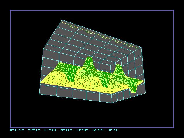
26 Simulation Specification Rise/Fall time Over/Under shoot Signal Losses Design file: 5ZONE3DUT_NOR.TLN BoardSim/LineSim, HyperLynx volts 1 V/div 0.0 volts Probe 1:C(J1) volts 0.000ns 50 nsec/div ns Date: Wednesday Dec. 15,1999 Cursor 1, Voltage = 3.41 V, Time = ns Cursor 2, Voltage = 3.03 V, Time = ns Delta Voltage = mv, Delta Time = ns 10/11/99 8
27 Simulation Cont Pre-Fabrication Simulation V/T graphs for all critical pins Adjust termination values Measure skew between signals Calculate Signal Integrity crosstalk 5% Accuracy between simulated and actual design Design file: 5ZONE3DUT_NOR.TLN BoardSim/LineSim, HyperLynx volts 1 V/div 0.0 volts Probe 1:C(J1) volts 0.000ns 50 nsec/div ns Date: Wednesday Dec. 15,1999 Cursor 1, Voltage = 3.41 V, Time = ns Cursor 2, Voltage = 3.03 V, Time = ns Delta Voltage = mv, Delta Time = ns 10/11/99 9
28 Simulation Cont 10/11/99 10
29 Simulation Cont 10/11/99 11
30 Simulation Cont 10/11/99 12
31 Simulation Cont BURN-IN BOARD MECHANICAL SPEC. OF THE CIRCUIT BOARD LAYER CONSTRUCTION LAYER 1 COMP 51 OHM 5 MIL PREPREG LAYER 2 GND 8 MIL CORE LAYER 3 INR 1 54 OHM 25 MIL PREPREG LAYER 4 INR 2 54 OHM 8 MIL CORE LAYER 5 VCC 5 MIL PREPREG LAYER 6 SOLD 51 OHM 1. All Cores are of 1oz Cu 2. Trace Width = 8 MILS 4. Over all board thickness 62 MILS +/-10% 5. Impedance is 50 Ohms +/-10% 6. Material is POLYIMIDE 7. Minimum distance b/w the Traces on COMP is 15 MILS 8. Minimum distance b/w the Traces on INR 1 & INR 2 is 25 MILS 9. Direction of Traces on INR 1 & INR 2 must be Perpendicular 10/11/99 13
32 Simulation Cont Pre-layout simulation What-if scenario Routing methodology for critical parameters Termination selection Component value estimation AC Term. DUT 500 Ohm PIN 10/11/99 14
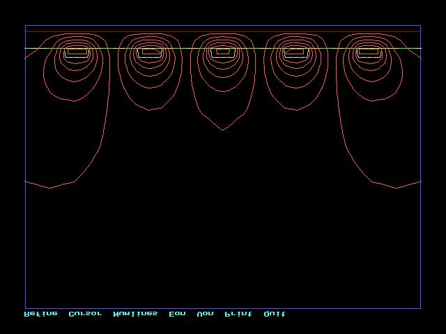
33 Simulation Cont Data Td = 2.15nS Clock Td = 3.45nS Skew = 1.3nS Data Td = 1.72nS Clock Td = 2.76nS Skew = 1.04nS Data Td = 1.23nS Clock Td = 2.1nS Skew = 0.87nS Data Td = 0.86nS Clock Td = 1.4nS Skew = 0.54nS Data Td = 0.43nS Clock Td = 0.72nS Skew = 0.29nS 15 MIL 15 MIL 15 MIL 15 MIL 15 MIL L=2" L=2.75" L=2" ck L=2.75" L=2" ck L=2.75" L=2" L=2.75" L=2" ck ck ck 15MIL L=5" CLOCK 1 50 GND 15 MILL L = 26" 15 MILL L = 42" CLOCK 2 CLOCK 3 12 MIL 15MIL 12 MIL 15MIL 12 MIL 15MIL 12 MIL 15MIL 12 MIL L=2" L=2.75" L=2" ck L=2.75" L=2" ck L=2.75" L=2" L=2.75" L=2" Data Td = 3.01nS Clock Td = 3.7nS Skew = 0.69nS ck ck ck Data Td = 3.44nS Clock Td = 4.38nS Skew = 0.94nS Data Td = 3.84nS Clock Td = 5.06nS Skew = 1.22nS Data Td = 4.3nS Clock Td = 5.75nS Skew = 1.45nS Data Td = 4.73nS Clock Td = 6.43nS Skew = 1.7nS 50 GND 15 MIL 13 MIL 13MIL 13 MIL 13 MIL 13 MIL 13 MIL 13 MIL 13 MIL 13 MIL L=2" L=2.75" L=2" ck L=2.75" L=2" ck L=2.75" L=2" L=2.75" L=2" ck ck ck 50 GND Data Td = 7.31nS Clock Td = 8.73nS Skew = 1.42nS Data Td = 6.88nS Clock Td = 8.05nS Skew = 1.17nS Data Td = 6.45nS Clock Td = 7.36nS Skew = 0.91nS Data Td = 6.02nS Clock Td = 6.68nS Skew = 0.66nS Data Td = 5.59nS Clock Td = 6nS Skew = 0.41nS 10/11/99 15
34 FAT Fabrication Number of layers, drill count/size and impedance requirement add to complexity Assembly Pin count, pin length and mounting affect assembly Test Design probe Verify actual board with schematic 10/11/99 16
35 Burn-In Board Design Considerations 2000 Burn-in and Test Sockets Workshop Tony Valente PCB Design Manager unisys
36 Agenda Mechanical Structures Clam shell ( shadow spacing ) Mounting hardware Electrical impact Pitch of pins Routing layers Through Hole Clam shell ( shadow spacing ) More stable mounting structure Surface Mount Buried vias Open routing paths Testability 10/11/9912/29/99 2 unisys
37 Mechanical Structures Clam Shell Shadow spacing Open Top Ability to move sockets closer than Clam Shell Creates access to heat removal Mounting Hardware Especially needed for SMT devices. Pin pitch Reduces manufacturability 10/11/9912/29/99 3 unisys
38 Calculating Shadow Spacing X = COS 85⁰ * X =.087 * X =.146 Shadow Spacing = Shadow Spacing =.540 Total distance between sockets would the length of the socket (1.555) plus the shadow spacing (.540). In this example the distance is minimum between sockets. 10/11/9912/29/99 4 unisys
39 Electrical Impact Pin pitch Tighter pitch decreases trace width (signal and power) Spacing between rows of pins (in QFPs) decreases routing space Hole diameter for pins (and pad size needed) decrease routing space Routing Layers Decreased trace width may mean using multiple routing layers for Power and Ground. With increased layer counts, overall board thickness will be effected. 10/11/9912/29/99 5 unisys
40 Through Hole vs. Surface Mount PROs More stable structure (pin vs vias) Access for all pins for testing. CONs Pin lead length Holes for all pins through board. PROs Blind vias would increase routing paths Easier to drill tolerance for vias vs pin diameter. Not limited by board thickness CONs Blind vias limit accessibility for test. More handling needed in assembly. 10/11/9912/29/99 6 unisys
March 4-7, 2018 Hilton Phoenix / Mesa Hotel Mesa, Arizona Archive
 March 4-7, 2018 Hilton Phoenix / Mesa Hotel Mesa, Arizona Archive 2018 BiTS Workshop Image: pilgrims49 / istock COPYRIGHT NOTICE The presentation(s)/poster(s) in this publication comprise the Proceedings
Session 2. Burn-in & Test Socket Workshop Socket Design
 Session 2 Burn-in & Test Socket Workshop 2000 Socket Design BURN-IN & TEST SOCKET WORKSHOP COPYRIGHT NOTICE The papers in this publication comprise the proceedings of the 2000 BiTS Workshop. They reflect
Board Design Guidelines for PCI Express Architecture
 Board Design Guidelines for PCI Express Architecture Cliff Lee Staff Engineer Intel Corporation Member, PCI Express Electrical and Card WGs The facts, techniques and applications presented by the following
I N T E R C O N N E C T A P P L I C A T I O N N O T E. STEP-Z Connector Routing. Report # 26GC001-1 February 20, 2006 v1.0
 I N T E R C O N N E C T A P P L I C A T I O N N O T E STEP-Z Connector Routing Report # 26GC001-1 February 20, 2006 v1.0 STEP-Z CONNECTOR FAMILY Copyright 2006 Tyco Electronics Corporation, Harrisburg,
Burn-in & Test Socket Workshop
 Burn-in & Test Socket Workshop IEEE March 4-7, 2001 Hilton Mesa Pavilion Hotel Mesa, Arizona IEEE COMPUTER SOCIETY Sponsored By The IEEE Computer Society Test Technology Technical Council COPYRIGHT NOTICE
Spring Probes and Probe Cards for Wafer-Level Test. Jim Brandes Multitest. A Comparison of Probe Solutions for an RF WLCSP Product
 AND, AT THE WAFER LEVEL For many in the industry, performing final test at the wafer level is still a novel idea. While providing some much needed solutions, it also comes with its own set of challenges.
Open NAND Flash Interface Specification: NAND Connector
 Open NAND Flash Interface Specification: NAND Connector Connector Revision 1.0 23-April-2008 Hynix Semiconductor Intel Corporation Micron Technology, Inc. Phison Electronics Corp. Sony Corporation Spansion
BGA Fanout Patterns. Charles Pfeil. Engineering Director Systems Design Division
 BGA Fanout Patterns Charles Pfeil Engineering Director Systems Design Division IPC Irvine Charles Pfeil Background 1966-1987 PCB Designer 1978-1987 Founder of Computer Circuits Inc., Fairfax VA, PCB Design
Burn-in & Test Socket Workshop WELCOME. March 2-5, 2003 Hilton Phoenix East / Mesa Hotel Mesa, Arizona
 Burn-in & Test Socket Workshop WELCOME March 2-5, 2003 Hilton Phoenix East / Mesa Hotel Mesa, Arizona Sponsored By The IEEE Computer Society Test Technology Technical Council tttc COPYRIGHT NOTICE The
Application Note 1242
 HFBR-5701L/5710L/5720L/5730L and HDMP-1687 Reference Design for 1.25 GBd Gigabit Ethernet and 1.0625 GBd Fiber Channel Applications Application Note 1242 Introduction Avago s objective in creating this
Best practices for EMI filtering and IC bypass/decoupling applications
 X2Y Component Connection and PCB Layout Guidelines Best practices for EMI filtering and IC bypass/decoupling applications X2Y Attenuators, LLC 1 Common X2Y Circuit Uses EMI FILTERING Conducted and Radiated
Celadon, Inc. TRX Series Infrared Remote and Receiver Assembly and Operation Instruction Manual
 Celadon, Inc. TRX Series Infrared Remote and Receiver Assembly and Operation Instruction Manual REV 2.1 COPYRIGHT 2001 I. Introduction Thank you for purchasing your infrared remote control transmitter
BiTS Poster Session. March 5-8, Hilton Phoenix / Mesa Hotel Mesa, Arizona. Archive Poster BiTS Workshop Image: tonda / istock
 March 5-8, 2017 Hilton Phoenix / Mesa Hotel Mesa, Arizona Archive Poster 2017 BiTS Workshop Image: tonda / istock Copyright Notice The presentation(s)/poster(s) in this publication comprise the Proceedings
2:1 MULTIPLEXER CHIP FOR PCI-EXPRESS ICS Description. Features. Block Diagram DATASHEET
 DATASHEET 2:1 MULTIPLEXER CHIP FOR PCI-EXPRESS ICS557-08 Description The ICS557-08 is a 2:1 multiplexer chip that allows the user to select one of the two HCSL (Host Clock Signal Level) or LVDS input pairs
User s Guide. Mixed Signal DSP Solutions SLLU011
 User s Guide July 2000 Mixed Signal DSP Solutions SLLU011 IMPORTANT NOTICE Texas Instruments and its subsidiaries (TI) reserve the right to make changes to their products or to discontinue any product
Lab 9 PCB Design & Layout
 Lab 9 PCB Design & Layout ECT 224L Department of Engineering Technology Lab 9 PCB Traces Size dependent upon electrical requirements, design constraints (routing space and clearance), and trace/space resolution
Preliminary Product Overview
 Preliminary Product Overview Features 1.0 A per channel / 3.0 A Total Current Maximum Voltage (AC or DC): +150 V Low On-State Resistance < 1.0 Ω 10 GΩ Input to Output Isolation < 10us Switching Time High
DAC348x PCB Layout Guidelines for the Multi-Row QFN package
 Texas Instruments Application Report DAC348x PCB Layout Guidelines for the Multi-Row QFN package Russell Hoppenstein Revision 1.0 Abstract This document provides additional information related to the multi-row
Probing Solutions for Logic Analyzers
 Probing Solutions for Logic Analyzers Catalog Create a Quality Connection to Your Target System To make sure you have the tools for dependable state and timing measurements, no matter what mix of chip
2:1 MULTIPLEXER CHIP FOR PCI-EXPRESS ICS Features
 DATASHEET 2:1 MULTIPLEXER CHIP FOR PCI-EXPRESS ICS557-08 Description The ICS557-08 is a 2:1 multiplexer chip that allows the user to select one of the two HCSL (Host Clock Signal Level) input pairs and
Hybrid Couplers 3dB, 90º Type PC2025A2100AT00
 GENERAL DESCRIPTION The PC2025A2100AT00 is a RoHS compliant low profile wideband 3dB hybrid coupler which can support mobile applications, including PCS and DCS applications. The power coupler series of
CENG 4480 Lecture 11: PCB
 CENG 4480 Lecture 11: PCB Bei Yu Reference: Chapter 5 of Ground Planes and Layer Stacking High speed digital design by Johnson and Graham 1 Introduction What is a PCB Why we need one? For large scale production/repeatable
I N T E R C O N N E C T A P P L I C A T I O N N O T E. STRADA Whisper 4.5mm Connector Enhanced Backplane and Daughtercard Footprint Routing Guide
 I N T E R C O N N E C T A P P L I C A T I O N N O T E STRADA Whisper 4.5mm Connector Enhanced Backplane and Daughtercard Footprint Routing Guide Report # 32GC001 01/26/2015 Rev 3.0 STRADA Whisper Connector
for Summit Analyzers Installation and Usage Manual
 Protocol Solutions Group PCI Express 2.0 Mid-Bus Probe for Summit Analyzers Installation and Usage Manual Manual Version 1.1 Generated on: 2/7/2018 6:25 PM Document Disclaimer The information contained
The System of Readout Boards for ALICE TRD
 PRESENTATION The System of Readout Boards for ALICE TRD Dr. Ivan Rusanov Physics Institute, Uni - Heidelberg ALICE TRD: Charge Sensitive Preamplifier (PASA Measurements - Dr. Ivan Rusanov; PI, Uni-Heidelberg)
I N T E R C O N N E C T A P P L I C A T I O N N O T E. Z-PACK TinMan Connector Routing. Report # 27GC001-1 May 9 th, 2007 v1.0
 I N T E R C O N N E C T A P P L I C A T I O N N O T E Z-PACK TinMan Connector Routing Report # 27GC001-1 May 9 th, 2007 v1.0 Z-PACK TinMan Connectors Copyright 2007 Tyco Electronics Corporation, Harrisburg,
Design For Manufacture
 Design For Manufacture Presented by Bill Frank Multek Applications Engineer Discussion Agenda Goals and Objectives DFM Process Flow Board Layout Analysis of Features Board Layout Yield Drivers Electrical
Area Array Probe Card Interposer. Raphael Robertazzi IBM Research 6/4/01. 6/4/01 IBM RESEARCH Page [1]
![Area Array Probe Card Interposer. Raphael Robertazzi IBM Research 6/4/01. 6/4/01 IBM RESEARCH Page [1]](/thumbs/78/78371092.jpg "Area Array Probe Card Interposer. Raphael Robertazzi IBM Research 6/4/01. 6/4/01 IBM RESEARCH Page [1]") Area Array Probe Card Interposer Raphael Robertazzi IBM Research 6/4/01 6/4/01 IBM RESEARCH Page [1] Motivation: Outline Probe Cards for Testing Complex ICs in the Developmental Stage. Hand Wired Space
Area Array Probe Card Interposer Raphael Robertazzi IBM Research 6/4/01 6/4/01 IBM RESEARCH Page [1] Motivation: Outline Probe Cards for Testing Complex ICs in the Developmental Stage. Hand Wired Space
Platform Design Guide
 Platform Design Guide Revision 1.1A Intel Corporation September 1997 THIS SPECIFICATION IS PROVIDED AS IS WITH NO WARRANTIES WHATSOEVER, INCLUDING ANY WARRANTY OF MERCHANTABILITY, NONINFRINGEMENT, FITNESS
Complete PCB Design Using OrCad Capture and Layout
 Complete PCB Design Using OrCad Capture and Layout By Kraig Mitzner Amsterdam Boston Heidelberg London New York Oxford Paris San Diego San Francisco Singapore Sydney Tokyo Newnes is an imprint of Elsevier
Revolutionary High Performance Interconnect Which Maximizes Signal Density
 Revolutionary High Performance Interconnect Which Maximizes Signal Density Tom Cohen and Gautam Patel Teradyne Connection Systems 44 Simon St. Nashua, New Hampshire 03060 Phone: 603-791-3383, 603-791-3164
Lecture 14: Prototyping and Schematics
 Lecture 14: Prototyping and Schematics Breadboards have some limitations They have high parasitic inductance and capacitance, limiting high frequency signal transfer to about 50MHz. Wire connections
Report # 20GC004-1 November 15, 2000 v1.0
 I N T E R C O N N E C T A P P L I C A T I O N N O T E Z-PACK HS3 Connector Routing Report # 20GC004-1 November 15, 2000 v1.0 Z-PACK HS3 6 Row 60 Position and 30 Position Connectors Copyright 2000 Tyco
ECE 5745 Complex Digital ASIC Design Topic 7: Packaging, Power Distribution, Clocking, and I/O
 ECE 5745 Complex Digital ASIC Design Topic 7: Packaging, Power Distribution, Clocking, and I/O Christopher Batten School of Electrical and Computer Engineering Cornell University http://www.csl.cornell.edu/courses/ece5745
Technical Note. Design Considerations when using NOR Flash on PCBs. Introduction and Definitions
 Technical Note Design Considerations when using NOR Flash on PCBs Introduction and Definitions TN-13-30: NOR Flash Memory: PCB Design Considerations Introduction and Definitions Table 1: Definitions Term
Burn-in & Test Socket Workshop
 Burn-in & Test Socket Workshop March 6-9, 2005 Hilton Phoenix East / Mesa Hotel Mesa, Arizona ARCHIVE TM Burn-in & Test Socket Workshop TM COPYRIGHT NOTICE The papers in this publication comprise the proceedings
IP1001 LF DESIGN & LAYOUT GUIDELINES
 Index 1 Purpose...2 2 Magnetic trace routing...2 3 Power Supply Plane & GND Plane...3 4 PHY interface...3 5 Trace routing & Placement...3 6 ESD protection...3 7 EMI Supression...3 1/7 April 17 2008. Ver:1.5
High-Speed Layout Guidelines for Reducing EMI for LVDS SerDes Designs. I.K. Anyiam
 High-Speed Layout Guidelines for Reducing EMI for LVDS SerDes Designs I.K. Anyiam 1 Introduction LVDS SerDes helps to reduce radiated emissions, but does not completely eliminate them EMI prevention must
Scope adapters and probes. Surface mount QFP Logic Analyzer adapters
 Logic Analyzer Adapters Logic Analyzer and scope adapters are designed to give access to each signal pin on a high-density IC. Some variations are specifically adapted to connect to a specific logic analyzer
KK1L 2x6 Antenna Switch Relay Controller / Dual Band Decoder Basic Assembly Version 4.8 (new 24-Aug-2009) Parts List updated 19-AUG-2016
 Parts List updated 19-AUG-2016") KK1L 2x6 Antenna Switch Relay Controller / Dual Band Decoder Basic Assembly Version 4.8 (new 24-Aug-2009) Parts List updated 19-AUG-2016 Ronald Rossi, KK1L http://home.comcast.net/~kk1l Design Features:
KK1L 2x6 Antenna Switch Relay Controller / Dual Band Decoder Basic Assembly Version 4.8 (new 24-Aug-2009) Parts List updated 19-AUG-2016 Ronald Rossi, KK1L http://home.comcast.net/~kk1l Design Features:
2 TO 4 DIFFERENTIAL CLOCK MUX ICS Features
 DATASHEET 2 TO 4 DIFFERENTIAL CLOCK MUX ICS557-06 Description The ICS557-06 is a two to four differential clock mux designed for use in PCI-Express applications. The device selects one of the two differential
250 Mbps Transceiver in LC FB2M5LVR
 250 Mbps Transceiver in LC FB2M5LVR DATA SHEET 650 nm 250 Mbps Fiber Optic Transceiver with LC Termination LVDS I/O IEC 61754-20 Compliant FEATURES LC click lock mechanism for confident connections Compatible
Orcad Layout Plus Tutorial
 Orcad Layout Plus Tutorial Layout Plus is a circuit board layout tool that accepts a layout-compatible circuit netlist (ex. from Capture CIS) and generates an output layout files that suitable for PCB
ST SPC58 B Line Emulation Adapter System
 _ V1.1 Hardware Reference ST SPC58 B Line Emulation Adapter ST SPC58 B Line Emulation Adapter System ST SPC58 B line emulation adapter primary use case is providing Nexus trace functionality for the SPC58
Symbol Parameter Min Typ Max VDD_CORE Core power 0.9V 1.0V 1. 1V. VDD33 JTAG/FLASH power 2.97V 3.3V 3.63V
 1 Introduction The user guide provides guidelines on how to help you successfully design the CME-M7 board which includes the power supply, configuration, clock, DDR2 or DDR3, high speed USB, LVDS and ADC
Keysight Technologies How to build a fixture for use with the Keysight Cover-Extend Technology. Application Note
 Keysight Technologies How to build a fixture for use with the Keysight Cover-Extend Technology Application Note Introduction Cover-Extend Technology (CET) is Keysight s latest limited access solution for
100GbE Architecture - Getting There... Joel Goergen Chief Scientist
 100GbE Architecture - Getting There... Joel Goergen Chief Scientist April 26, 2005 100GbE Architecture - Getting There Joel Goergen Force10 Networks joel@force10networks.com Subject : 100GbE Architecture
ARCHIVE Kelvin Contacting Jim Brandes Everett Charles Technologies
 Poster Session ARCHIVE 8 Kelvin Contacting Jim Brandes Everett Charles Technologies Use Simulation to Obtain S Parameters and Network Parameters for Sockets and PCB/Connectors Sultan Faiz, Mike Fedde Ironwood
Vertical Conductive Structures
 Vertical Conductive Structures A new Interconnect Technique Agenda The need for an alternative PCB technology Introduction of VeCS Technology comparison Cost comparison State of VeCS technology Application
Multi-Drop LVDS with Virtex-E FPGAs
 Multi-Drop LVDS with Virtex-E FPGAs XAPP231 (Version 1.0) September 23, 1999 Application Note: Jon Brunetti & Brian Von Herzen Summary Introduction Multi-Drop LVDS Circuits This application note describes
NB3H83905CDGEVB. NB3H83905CDGEVB Evaluation Board User's Manual EVAL BOARD USER S MANUAL
 NB3H83905CDGEVB Evaluation Board User's Manual EVAL BOARD USER S MANUAL Device Description The NB3H83905CDG device is a 1.8 V, 2.5 V or 3.3 V VDD core Crystal input 1:6 LVTTL/LVCMOS fanout buffer with
Board Design Guidelines for Intel Programmable Device Packages
 Board Design Guidelines for Intel Programmable Device Packages AN-114 2017.02.24 Subscribe Send Feedback Contents Contents 1 Board Design Guidelines for Intel Programmable Device Packages...3 1.1 Overview
ONE STOP SOLUTION FOR YOUR EMBEDDED SYSTEMS NEEDS
 ONE STOP SOLUTION FOR YOUR EMBEDDED SYSTEMS NEEDS 39/B, Yogashram Society, Behind Manekbaug Society, Ahmedabad 380015, INDIA TEL - +91-9825366832 EMAIL: gaurav_jogi@yahoo.co.in URL: http://gjmicrosys.tripod.com
Physical Implementation
 CS250 VLSI Systems Design Fall 2009 John Wawrzynek, Krste Asanovic, with John Lazzaro Physical Implementation Outline Standard cell back-end place and route tools make layout mostly automatic. However,
- create new schematic to the new project, PCB design begins with a schematic diagram, which present how components are connected
 Eagle 8.x tutorial - create a new project, Eagle designs are organized as projects - create new schematic to the new project, PCB design begins with a schematic diagram, which present how components are
Transcendent Frequency Counter
 Transcendent Frequency Counter with blue 2 x 16 LCD display This manual will guide you how to assemble, test and operate this frequency counter KIT. Features: The transcendent counter has two input channels
SFC ChipClamp ΤΜ Flip Chip TVS Diode with T-Filter PRELIMINARY Features
 Description The SFC2282-50 is a low pass T-filter with integrated TVS diodes. It is designed to provide bidirectional filtering of EMI/RFI signals and electrostatic discharge (ESD) protection in portable
Socket Mounting Recommendations and Reflow Profile
 Purpose This document is meant to serve as a guide for mounting E-tec surface mount device (SMD) sockets to the printed circuit board (PCB). The recommendations described here are guidelines only, and
Wafer Level Packaging The Promise Evolves Dr. Thomas Di Stefano Centipede Systems, Inc. IWLPC 2008
 Wafer Level Packaging The Promise Evolves Dr. Thomas Di Stefano Centipede Systems, Inc. IWLPC 2008 / DEVICE 1.E+03 1.E+02 1.E+01 1.E+00 1.E-01 1.E-02 1.E-03 1.E-04 1.E-05 1.E-06 1.E-07 Productivity Gains
IDT PEB383 QFP Board Design Guidelines
 IDT PEB383 QFP Board Design Guidelines February 2010 6024 Silver Creek Valley Road, San Jose, California 95138 Telephone: (800) 345-7015 (408) 284-8200 FAX: (408) 284-2775 Printed in U.S.A. 2009 GENERAL
DM9051NP Layout Guide
 NP Version: 1.1 Technical Reference Manual Davicom Semiconductor, Inc Version: NP-LG-V11 1 1. Placement, Signal and Trace Routing Place the 10/100M magnetic as close as possible to the (no more than 20mm)
Using Valor Trilogy to Generate 5DX Program Files
 Using Valor Trilogy to Generate 5DX Program Files Introduction NBS > Printed Circuit Board Design > Printed Circuit Board Assembly > Printed Circuit Board Test 5DX Programming 5DX Board Testing Agenda
Over 5,000 products High Performance Adapters and Sockets Many Custom Designs Engineering Electrical and Mechanical ISO9001:2008 Registration
 Overview Company Overview Over 5,000 products High Performance Adapters and Sockets Many Custom Designs Engineering Electrical and Mechanical ISO9001:2008 Registration Adapter Technology Overview Pluggable
Skill Development Centre by AN ISO CERTIFIED COMPANY
 Skill Development Centre by AN ISO CERTIFIED COMPANY Industrial Automation Training Embedded/ VLSI system design Electrical control panel Design Product Development Fiber optics Technician Electrician
Joe Birtola CMR Summit Technologies. High Frequency PCB Material Characterization and Simulation. Ryan Satrom Multitest
 BRING IT TO THE BOARD (PCB) The device under test (DUT) board is sometimes overlooked as a critical element in test-and burn-in strategies. This session brings PCBs into the limelight. The first presentation
March 15-18, 2015 Hilton Phoenix / Mesa Hotel Mesa, Arizona Archive Session 8
 Proceedings March 15-18, 2015 Hilton Phoenix / Mesa Hotel Mesa, Arizona Archive Session 8 2015 BiTS Workshop Image: BCFC/iStock Proceedings Session 8 Morten Jensen Session Chair BiTS Workshop 2015 Schedule
Products, Services & Capabilities
 Products, Services & Capabilities Toll Free: (800) 404-0204 U.S. Only Tel: (952) 229-8200 Fax: (952) 229-8201 email: info@ironwoodelectronics.com Overview Company Overview Founded 1986 Over 5,000 products
Elma Bustronic CompactPCI Reference Sheet
 Elma Bustronic CompactPCI Reference Sheet Rev. 4 5.10.10 The cpci reference sheet provides relevant reference material for the CompactPCI product line. The information provided may change at anytime. Elma
Adapter Technologies
 Adapter Technologies Toll Free: (800) 404-0204 U.S. Only Tel: (952) 229-8200 Fax: (952) 229-8201 email: info@ironwoodelectronics.com Introduction Company Overview Over 5,000 products High Performance Adapters
PCIe 3.0 Clock Generator with 4 HCSL Outputs. Description OE VDDXD S0 S1 S2 X1 X2 PD OE GNDXD IREF CLK0 CLK0 CLK1 CLK1 CLK2 CLK2 CLK3 CLK3
 PCIe 3.0 Clock Generator with 4 HCSL Outputs Features PCIe 3.0 complaint PCIe 3.0 Phase jitter: 0.48ps RMS (High Freq. Typ.) LVDS compatible outputs Supply voltage of 3.3V ±5% 25MHz crystal or clock input
PRODUCT SPECIFICATION
 SIM Card Connector, Hinged Type, 8 Pin, SMT, 1.50mm Profile. Page 1 SIM Card Connector, Hinged Type, 8 Pin, SMT, 1.50mm Profile. Page 2 1.0 SCOPE. This specification covers performance, tests and quality
E-tec Socketing solutions for BGA, LGA, CGA, CSP, MLF & Gullwing chips
 E-tec Socketing solutions for BGA, LGA, CGA, CSP, MLF & Gullwing chips Available contact styles: Elastomer interposers (10 Ghz & more) Probe pin sockets (generally below 5 Ghz) Other interposer styles
PI6C557-01BQ. PCIe 3.0 Clock Generator with 1 HCSL Outputs. Features. Description. Pin Configuration (16-Pin TQFN) Block Diagram
 Block Diagram") s Features ÎÎPCIe 3.0 compliant à à Phase jitter - 0.45ps RMS (High Freq. Typ.) ÎÎLVDS compatible output ÎÎSupply voltage of 3.3V ±10% ÎÎ25MHz crystal or clock input frequency ÎÎHCSL outputs, 0.8V Current
s Features ÎÎPCIe 3.0 compliant à à Phase jitter - 0.45ps RMS (High Freq. Typ.) ÎÎLVDS compatible output ÎÎSupply voltage of 3.3V ±10% ÎÎ25MHz crystal or clock input frequency ÎÎHCSL outputs, 0.8V Current
24DSI16WRC Wide-Range 24-Bit, 16-Channel, 105KSPS Analog Input Module With 16 Wide-Range (High-Level, Low-Level) Delta-Sigma Input Channels
 Delta-Sigma Input Channels") 24DSI16WRC Wide-Range 24-Bit, 16-Channel, 105KSPS Analog Input Module With 16 Wide-Range (High-Level, Low-Level) Delta-Sigma Input Channels Features Include: Available in PMC, PCI, cpci and PC104-Plus
24DSI16WRC Wide-Range 24-Bit, 16-Channel, 105KSPS Analog Input Module With 16 Wide-Range (High-Level, Low-Level) Delta-Sigma Input Channels Features Include: Available in PMC, PCI, cpci and PC104-Plus
Patented socketing system for the BGA/CSP technology
 Patented socketing system for the BGA/CSP technology Features: ZIF handling & only 40 grams per contact after closing the socket Sockets adapt to all package styles (at present down to 0.40mm pitch): Ceramic
Introduction to Wafer Level Burn-In. William R. Mann General Chairman Southwest Test Workshop
 Introduction to Wafer Level Burn-In William R. Mann General Chairman Southwest Test Workshop Outline Conventional Burn In and Problems Wafer Level BI Driving Factors Initial Die Level BI Technical Challenges
HSP061-4M10. 4-line ESD protection for high speed lines. Datasheet. Features. Applications. Description
 Datasheet 4-line ESD protection for high speed lines Features I/O I/O 2 GND 3 I/O 3 I/O 4 2 4 µqfn-0l package Functional schematic (top view) 0 9 8 7 5 6 Product status HSP06-4M0 Internal ly not connected
High-Speed DDR4 Memory Designs and Power Integrity Analysis
 High-Speed DDR4 Memory Designs and Power Integrity Analysis Cuong Nguyen Field Application Engineer cuong@edadirect.com www.edadirect.com 2014 1 PCB Complexity is Accelerating Use of Advanced Technologies
MDI for 4x25G Copper and Fiber Optic IO. Quadra (CFP4 proposal) Connector System
 Connector System") MDI for 4x25G Copper and Fiber Optic IO Quadra (CFP4 proposal) Connector System Nov 7, 2011 Nathan Tracy, TE Connectivity Tom Palkert, Molex 4x25Gb/s MDI Potential Requirements Critical Needs: Excellent
MDI for 4x25G Copper and Fiber Optic IO Quadra (CFP4 proposal) Connector System Nov 7, 2011 Nathan Tracy, TE Connectivity Tom Palkert, Molex 4x25Gb/s MDI Potential Requirements Critical Needs: Excellent
Control Circuitry 2 M1. Micrel Inc Fortune Drive San Jose, CA USA tel +1 (408) fax + 1 (408)
 fax + 1 (408)") Crystal-less Configurable Clock Generator General Description The is a programmable, high performance dual LVDS output oscillator utilizing Micrel's proven silicon MEMS technology to provide excellent
Crystal-less Configurable Clock Generator General Description The is a programmable, high performance dual LVDS output oscillator utilizing Micrel's proven silicon MEMS technology to provide excellent
PRA Inc th Place NE Arlington, WA U.S.A.
 2360 Series Quartz Crystal - Oscillator Aging and Aging Measurement Test System Devices are operating while aging Frequency Measurement made while aging Up to 4000 devices simultaneously in a Model 2360
GuitarPCB.com Mini-Me Chorus Build Instructions
 GuitarPCB.com Mini-Me Chorus Build Instructions This compares to the popular Small Clone TM chorus, but includes modifications. The major difference between this circuit and the commercial pedal on which
Model XDL S Rev A
 Delay Line DESCRIPTION The XDL15-3-030S can be used in amplifier linearization applications from 135 2700Mhz. Small form factor of XDL15-3-030S is ideal for cascading to obtain longer delay. The Xinger
Frequency Generator for Pentium Based Systems
 Integrated Circuit Systems, Inc. ICS969C-23 Frequency Generator for Pentium Based Systems General Description The ICS969C-23 is a low-cost frequency generator designed specifically for Pentium-based chip
Implementing Bus LVDS Interface in Cyclone III, Stratix III, and Stratix IV Devices
 Implementing Bus LVDS Interface in Cyclone III, Stratix III, and Stratix IV Devices November 2008, ver. 1.1 Introduction LVDS is becoming the most popular differential I/O standard for high-speed transmission
VITA 67 Series. Ideal For Blind Mate Applications. Electrical, Mechanical & Environmental Specifications
 VITA 67 Series Delta Electronics Manufacturing Corp. introduces 4 position (VITA 67.1) and 8 position (VITA 67.2) RF connector housings designed for 3U and 6U formats within the OpenVPX architecture. Ideal
6 Channel EMI Filter Array with ESD Protection
 6 Channel EMI Filter Array with ESD Protection Features Six channels of EMI filtering for data ports Pi-style EMI filters in a capacitor-resistor-capacitor (C-R-C) network Greater than 32dB attenuation
OSFP Connector Cage & Cable System
 PAGE /6 /5/7 UNRESTRICTED OSFP Connector Cage & Cable System PAGE /6 /5/7 UNRESTRICTED.0 SCOPE This Product Specification covers performance, test and quality requirements for the JPC Quad Small Form Factor
RClamp3328P. Low Capacitance RClamp. 8-Line Protection PRELIMINARY
 PROTECTION PRODUCTS - RailClamp Description The RClamp provides low voltage ESD protection for high-speed ports. It features a high maximum ESD withstand voltage of ±25kV contact and ±3kV air discharge
2.5 V/3.3 V, 8-Bit, 2-Port Level Translating, Bus Switch ADG3245
 V/3.3 V, 8-Bit, 2-Port Level Translating, Bus Switch ADG3245 FEATURES 225 ps Propagation Delay through the Switch 4.5 Switch Connection between Ports Data Rate 1.244 Gbps V/3.3 V Supply Operation Selectable
Additional Slides for Lecture 17. EE 271 Lecture 17
 Additional Slides for Lecture 17 Advantages/Disadvantages of Wire Bonding Pros Cost: cheapest packages use wire bonding Allows ready access to front side of die for probing Cons Relatively high inductance
PRODUCT SPECIFICATION
 SIM Card Connector, Hinged Type, 6 Pin, SMT, 1.85mm Profile. Page 1 SIM Card Connector, Hinged Type, 6 Pin, SMT, 1.85mm Profile. Page 2 1.0 SCOPE. This specification covers performance, tests and quality
HSP line ESD protection for high speed lines. Applications. Description. Features. µqfn 4 leads. Benefits. Complies with following standards
 2-line ESD protection for high speed lines Datasheet - production data Benefits High ESD robustness of the equipment Suitable for high density boards Complies with following standards MIL-STD 883G Method
TF90LVDS047-6CG. Quad LVDS Line Driver with Flow-Through Pinout. Description. Features. Applications. Function Diagram. Ordering Information
 Features Companion driver to Quad Extended Common Mode LVDS Receiver TF0LVDS048 DC to 400 Mbps / 200 MHz low noise, low skew, low power operation t 350 ps (max) channel-to-channel skew t 250 ps (max) pulse
I N T E R C O N N E C T A P P L I C A T I O N N O T E. Advanced Mezzanine Card (AMC) Connector Routing. Report # 26GC011-1 September 21 st, 2006 v1.
 Connector Routing. Report # 26GC011-1 September 21 st, 2006 v1.") I N T E R C O N N E C T A P P L I C A T I O N N O T E Advanced Mezzanine Card (AMC) Connector Routing Report # 26GC011-1 September 21 st, 2006 v1.0 Advanced Mezzanine Card (AMC) Connector Copyright 2006
I N T E R C O N N E C T A P P L I C A T I O N N O T E Advanced Mezzanine Card (AMC) Connector Routing Report # 26GC011-1 September 21 st, 2006 v1.0 Advanced Mezzanine Card (AMC) Connector Copyright 2006
Achieving EMV Electrical Compliance with the Teridian 73S8024RN
 August 2005 Achieving EMV Electrical Compliance with the Teridian 1 Introduction This application note highlights particular testing considerations required to achieve compliance for payment systems smart
Bolero Nexus Emulation Adapter 208BGA 100TQ
 _ V1.5 Adapters Bolero Nexus Emulation Adapter 208BGA 100TQ Ordering code IA208BGA100TQ-5607B Supported microcontrollers: Freescale MPC5605B, MPC5605BK, MPC5606BK ST equivalent devices (SPC560B54, SPC560B60)
MIPI D-PHY REFERENCE TERMINATION BOARD (RTB) OVERVIEW AND DATASHEET
 OVERVIEW AND DATASHEET") The InterOperability Laboratory MIPI D-PHY REFERENCE TERMINATION BOARD (RTB) OVERVIEW AND DATASHEET Abstract: This document serves as the primary documentation for the MIPI D-PHY Reference Termination
The InterOperability Laboratory MIPI D-PHY REFERENCE TERMINATION BOARD (RTB) OVERVIEW AND DATASHEET Abstract: This document serves as the primary documentation for the MIPI D-PHY Reference Termination
W5100 Layout Guide version 1.0
 version 1.0 2009 WIZnet Co., Inc. All Rights Reserved. For more information, visit our website at http://www.wiznet.co.kr Copyright 2009 WIZnet Co., Inc. All rights reserved. Table of Contents 1 Goal...
ECE 497 JS Lecture - 21 Noise in Digital Circuits
 ECE 497 JS Lecture - 21 Noise in Digital Circuits Spring 2004 Jose E. Schutt-Aine Electrical & Computer Engineering University of Illinois jose@emlab.uiuc.edu 1 Announcements - NL05 program available -