Advanced Packaging For Mobile and Growth Products
|
|
|
- Dorothy Powers
- 5 years ago
- Views:
Transcription

1 Advanced Packaging For Mobile and Growth Products Steve Anderson, Senior Director Product and Technology Marketing, STATS ChipPAC
2 Growing Needs for Silicon & Package Integration Packaging Trend Implication to OSAT Computing US$125.4B US$136.1B % CAGR Communication US$70.3B US$80.9B % CAGR Converged Market Mobile Computing Convergent Products US$28.8B 37.5% CAGR 2D SoC QFN, FBGA, fcbga, fcfbga, ewlb, WLCSP 3D SIP PoP/PiP, FBGA-SD, ISM, Module Pressure on packaging cost Needs for best valued BOM More flip chip & WLP (capital intensive) Yield & cycle time Die thinning & stacking Advanced multi-tiers wire bonding Passives discrete handling or IPD Yield & cycle time 3D IC F/BGA-TSV-SD, PoP- TSV, ewlb, IPD Capital intensive Silicon interface know-how 2.5D IC using Si interposer Yield & cycle time New converged applications require more complex & customized packaging solutions 2


3 Heterogeneous integration; advanced 3D PKG solutions Micro Electronics Die Area Reduction MEMS RF Photonics CMOS IC to 22nm & Beyond IC & 3D Module & 3D IC Pkg: ewlb/ Fanout Wafer Level PKG 3D IC Systems with TSV Sensors Design Nano-Materials & Components System Interconnections Thermal Consumer Electronics Energy Automotive Healthcare Computing & Communications 3


4 Drivers for Mobile /Portable Device Packaging Size (area and thickness) Performance Cost Standardized Reliability Environmental 4
 Many Billions of Packages Shipped")


5 More and More WLCSPs in mobile phones WLCSP (wafer level CSP) Many Billions of Packages Shipped Established worldwide Industry Infrastructure Lead free & MSL1 I/O ranging Smart Phone WLCSP Statistics Apple iphone 48 dies - 21% are WLCSP RIM Blackberry Storm 42 dies - 29% are WLCSP Nokia dies - 50% are WLCSP 5

6 Advanced Wafer Level Integration Technology Evolution LEADED PACKAGING ARRAY PACKAGING EMBEDDED & 3D PACKAGING Advanced node compatibility Large Scale Low cost ewlb 3D TSV ICs Higher integration Performance Reliability Design Flexibility TSV Interposer 6

")
 & PiP")


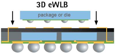
7 Evolu&on of 3D Packages TSV stacked 8G DDR3, 2011 Integration, Density, Performance (24 die-stack) Stacked Die Stacked Packages PoP (ewlb) & PiP Ultra low profile ewlb+mlp Stacked die 2.5D/3D TSV 3D ewlb TSV interposer 2011 Production Development Manufacturing Maturity 7 7
8 Portable/Mobile Electronics- Package Trends - Stacked Die Packages - Package on Package (PoP) - ewlb / FO-WLP / EDS - Through Silicon Vias (TSV) 3D Chip Packaging Solutions SiP System in package SoP System on package (High Density Heterogeneous / Modular Chips Integration) SoC System on chip (Single Chip- Chip Level Integration) Chip packaging compatibility with SMT assembly process 3S Reliability 3S Assembly process, material and rework 8

9 Silicon Interposer Delivers High Interconnect Density 9

10 ewlb and Wafer Level Packaging Technology 10
 Lateral dimensions (ò ) I/O Density Pitches (ò ) Min pitches No standards Small chips/ high no. of I/Os Wafer Level Packages Min line length Multilayer RDL Reduced no.")
11 Driving Forces to Wafer Level Package Cost Packaging cost Test cost Batch processing High parallelism Improved test concepts Smallest package heights Minimum lateral area Dimensions Package height (ò ) Lateral dimensions (ò ) I/O Density Pitches (ò ) Min pitches No standards Small chips/ high no. of I/Os Wafer Level Packages Min line length Multilayer RDL Reduced no. of interconnects Electrical Performance Interconnect line length (ò ) Operating frequencies (ñ ) Package Speed (ñ ) Parasitics Functionality (Integration) Integrated Passives (R, L, C) System in Package 3D Integrated passives in RDL SiP/ 3D capability Improved chip to board coupling Thermal Performance Power consumption (ñ ) Package Density (ñ ) 11

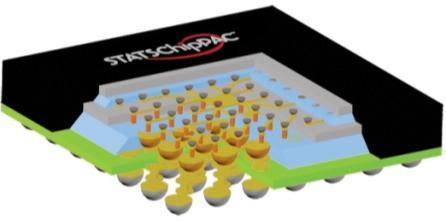
12 What is ewlb? A new Wafer Level Packaging technology, utilizes well developed wafer bumping infrastructure, with an innovative wafer reconstitution process to package Known Good Dice. Wafer level package, uses mold compound to support the fan-out I/Os. Fan-In WLP PKG size = Chip size ewlb/fan-out WLP PKG size > Chip size chip chip Fan-In Interconnects only - Number and pitch of Interconnects must be adapted to the chip size Only Single chip packaging solution ewlb expands the application space for Wafer Level Packaging! 12 Fan-out Interconnects - #, Pitch of Interconnect is INDEPENDENT of chip size Single/Multi/3D chip packaging solution Improved Yield with KGD


 Cu/ELK compatible")
 Green")
 Superior board level")


13 Advantages of ewlb Technology Thinner & smaller package solution Ideal for mobile applications and meeting future roadmaps Package robustness (vs. LF flip chip + advanced fab nodes with ELK) Cu/ELK compatible packaging technology (65nm in HVM, 40nm in Qualification) Green packaging (Generic Pb-free, Halogen free) Superior board level reliability proven for mobile applications Proven lower cost path using a batch process & simpler supply chain Next generation ewlb technology with 3D ewlb joint development No substrate or bumping; Simple logistics and supply chain 13 Solder ball Cu-RDL Si Chip EMC


14 ewlb Products Portfolio 2D ewll 2.5D / Extended ewlb ewlb- MLP 14


 Plated Cu")


")
15 Next Generation ewlb 10 m/10 m line width and line spacing Thin packaging solution (<0.5mm) Plated Cu RDL 10 m 250 m thin ewlb for more design and routing flexibility Embedded Passives 3D (double-side) ewlb Multi-die ewlb 15
 + 3x4mm) I/O Count: 396 1-L RDL 2-die ewlb PKG: 12x12sqmm,")


16 Multi-Die ewlb (Side-by-side) 3-die ewlb PKG: 12x12sqmm, 0.5mm ball pitch Die : 3-die, 2 (3x3mm) + 3x4mm) I/O Count: L RDL 2-die ewlb PKG: 12x12sqmm, 0.4mm ball pitch Die: 4x4mm (2 dies) I/O Count: L RDL Reliability Test Pre-condition Test Condition Read-out Pass Multiple Reflow - LF 260 o C 5x, 10x, 20x passed Unbiased HAST MSL1 130 o C, 85%RH 96hr passed Temperature Cyc ling MSL1-55 o C/125 o C (G) 500x, 850x passed 2-die ewlb PKG: 8x8 sqmm, 0.5mm ball pitch Die : 2-die, 2 (5x2.5 mm) I/O Count: L RDL High Temp. Stor age MSL1 150 o C 500, 1000hr passed TCoB -40/125C 500x passed Drop test Nokia Spec - passed Highly integrated SiP or side-by-side packaging solution with multidie. Can be integrated with IPD, RDL passives or discrete MLCCs. 16
 + 3x4mm) I/O Count: 396 1-L RDL (Top and Bottom both) Thickness 450um / 250um Passed")
 with less than 1mm thickness including solder balls.")
17 Double-side 3D ewlb Package Specification PKG: 12x12sqmm, 0.5mm ball pitch Die : 3-die, 2 (3x3mm) + 3x4mm) I/O Count: L RDL (Top and Bottom both) Thickness 450um / 250um Passed JEDEC component level and board level reliability tests 1.2mm 250um Thin Bottom 3D PKG 450um 250um <1.0mm Low profile 3D ewlb PoP (12x12mm PoP-bottom package) with less than 1mm thickness including solder balls. 17 Picture of 3D ewlb PoP packages; Total less than 1.0 mm package height (including solder balls)
 Low warpage during solder reflow cycles Larger Si die")
 Q JB 3~7( o C/W) for 12x12mm ewmlp) 18 Memory")
18 Ultra Low Profile ewlb PoP: ewlb-mlp (embedded Wafer level Molded Laser PoP) ewlb MLP ewlb-mlp Thin POP (250um pkg body thickness) Low warpage during solder reflow cycles Larger Si die cavity Flexibility in memory interface High routing density: L/S=10/10 (um) Compatible with ELK Good thermal performance Q JA 18~22( o C/W) Q JB 3~7( o C/W) for 12x12mm ewmlp) 18 Memory + Si RDL
19 ewlb : Themo-Moire, High Temperature Warpage Measurement fcvfbga,7x7mm, 191LD NSP PKG height 0.95 mm Die 4.46 x 5.65 x 0.19 mm ewlb 8x8mm, 182I/O PKG height 0.7 mm Die 5 x 5 x 0.45 mm 19


20 TSV Technology 3D IC TSV 2.5D Interposer 20

: Thermal Compression with NCP Thin wafer handling and packaging")
21 TSV Technology for mobile devices (Logic + Memory) Wide I/O memory interface in mobile - Examples: AP+DRAM or AP/BB combo+dram in mobile devices High Performance Devices High electrical performance solution : Increasing number of I/Os Power effective solution : Minimized output loading with CtC connection TSV for shorter interconnection length for better performance Micro-bump Micro-bump bonding (50/40um pitch): Thermal Compression with NCP Thin wafer handling and packaging TSV 21
 & higher performance For embedded memory; Nominal LSI Memory capacity 2X per node edram shrinks <")
 Heterogeneous integration in Pkg 2D - SoC 2.")
22 TSV Technology for high performance processors: Examples: GPU + DRAM, MPU + DRAM, Logic + Analog, sliced FPGA integration Lower cost (High yield) & higher performance For embedded memory; Nominal LSI Memory capacity 2X per node edram shrinks < 40% per node Total memory area grows node to node edram capacity (Mb) needs 130nm 90nm 65nm 45nm De-couple functional blocks in SoC (analogue, memory, I/O, RF, ) Heterogeneous integration in Pkg 2D - SoC 2.5D TSV interposer 3D TSV in Device 22
 of 40um pitch with Cu column")


23 Thermo-compression Bonding Thermo-compression Bonding (TCB) of 40um pitch with Cu column and NCP (non-conductive paste) Chip-to-Chip 40/50um pad pitch with ENIG pad finish on Cu pad Chip-to-Substrate 40um pitch Cu column on Substrate 23 No void observed after TCB with NCP)

24 TSV Silicon Interposer (TSI) Technology Provide High Complexity, High Performance ASICs with Dependable Predictability Technology Disaggregation Optimization of Silicon Technology for Individual IP Higher Levels of System Integration Wider Product Capability Offering to Customers Lower Total System Power 24

25 TSV Silicon Interposer (TSI) Technology - Con&nued External Memory Solutions Increase Memory Options for Customers Increase Memory Storage per ASIC Low Power and Higher Bandwidth Leverage Industry Standard Memories Die Separation Decrease Yield Losses of Large Die Decrease Yield Losses Early in 25


26 Func&onal Par&&oning with TSI Heterogeneous Integration Silicon interposer advantages Reduced die complexity Mixed technologies Source: Xilinx 2.5D FPGA 26
27 2.5D and 3D will Coexist? 3D especially with TSVs is a revolutionary change requiring significant infrastructure additions. 2.5D allows use of mixed interconnect ICs from different sources and is evolutionary. 2.5D may become as essential within a package assembly as underfill epoxy for both single chips and stacked 3D chips. 2.5D is not limited to silicon glass and even organic solutions provide economical benefits in applications where silicon is inappropriate. 27
28 Summary Wafer level packaging is a key technology enabler for future heterogeneous integration. Next generation and 3D ewlbs would be a good solution for future needs in mobile/portable applications, such as PoP and 3D SiP. With scale-up and higher throughput, large panel approach is next step for further market-penentration as cost-effective packaging solutions. TSV technology is critical for continued evolution of semiconductor industry. TSV interposer technology is one of early application of TSV technology. As with all new technologies for 2.5D/3D TSV wafer level integration; Product applications & drivers are critical. Alternative technology, ewlb technology, wafer level packaging solution enabling 3D wafer level integration with low cost solution. More collaborative cost/ performance analysis across FE-BE FAB, EDA, Assembly, Reliability, Metrology & Test are needed for successful TSV biz establishment. 28
29 Thank You
TechSearch International, Inc.
 Alternatives on the Road to 3D TSV E. Jan Vardaman President TechSearch International, Inc. www.techsearchinc.com Everyone Wants to Have 3D ICs 3D IC solves interconnect delay problem bandwidth bottleneck
Multi-Die Packaging How Ready Are We?
 Multi-Die Packaging How Ready Are We? Rich Rice ASE Group April 23 rd, 2015 Agenda ASE Brief Integration Drivers Multi-Chip Packaging 2.5D / 3D / SiP / SiM Design / Co-Design Challenges: an OSAT Perspective
Vertical Circuits. Small Footprint Stacked Die Package and HVM Supply Chain Readiness. November 10, Marc Robinson Vertical Circuits, Inc
 Small Footprint Stacked Die Package and HVM Supply Chain Readiness Marc Robinson Vertical Circuits, Inc November 10, 2011 Vertical Circuits Building Blocks for 3D Interconnects Infrastructure Readiness
TechSearch International, Inc.
 On the Road to 3D ICs: Markets and Solutions E. Jan Vardaman President TechSearch International, Inc. www.techsearchinc.com High future cost of lithography Severe interconnect delay Noted in ITRS roadmap
Advanced Flip Chip Package on Package Technology for Mobile Applications
 Advanced Flip Chip Package on Package Technology for Mobile Applications by Ming-Che Hsieh Product and Technology Marketing STATS ChipPAC Pte. Ltd. Singapore Originally published in the 17 th International
Packaging Innovation for our Application Driven World
 Packaging Innovation for our Application Driven World Rich Rice ASE Group March 14 th, 2018 MEPTEC / IMAPS Luncheon Series 1 What We ll Cover Semiconductor Roadmap Drivers Package Development Thrusts Collaboration
Bringing 3D Integration to Packaging Mainstream
 Bringing 3D Integration to Packaging Mainstream Enabling a Microelectronic World MEPTEC Nov 2012 Choon Lee Technology HQ, Amkor Highlighted TSV in Packaging TSMC reveals plan for 3DIC design based on silicon
Ultra Fine Pitch RDL Development in Multi-layer ewlb (embedded Wafer Level BGA) Packages
 Packages") Ultra Fine Pitch RDL Development in Multi-layer ewlb (embedded Wafer Level BGA) Packages Won Kyoung Choi*, Duk Ju Na*, Kyaw Oo Aung*, Andy Yong*, Jaesik Lee**, Urmi Ray**, Riko Radojcic**, Bernard Adams***
Ultra Fine Pitch RDL Development in Multi-layer ewlb (embedded Wafer Level BGA) Packages Won Kyoung Choi*, Duk Ju Na*, Kyaw Oo Aung*, Andy Yong*, Jaesik Lee**, Urmi Ray**, Riko Radojcic**, Bernard Adams***
3-D Package Integration Enabling Technologies
 3-D Package Integration Enabling Technologies Nanium - Semi Networking Day David Clark - Choon Heung Lee - Ron Huemoeller June 27th, 2013 Enabling a Microelectronic World Mobile Communications Driving
WLSI Extends Si Processing and Supports Moore s Law. Douglas Yu TSMC R&D,
 WLSI Extends Si Processing and Supports Moore s Law Douglas Yu TSMC R&D, chyu@tsmc.com SiP Summit, Semicon Taiwan, Taipei, Taiwan, Sep. 9 th, 2016 Introduction Moore s Law Challenges Heterogeneous Integration
Innovative 3D Structures Utilizing Wafer Level Fan-Out Technology
 Innovative 3D Structures Utilizing Wafer Level Fan-Out Technology JinYoung Khim #, Curtis Zwenger *, YoonJoo Khim #, SeWoong Cha #, SeungJae Lee #, JinHan Kim # # Amkor Technology Korea 280-8, 2-ga, Sungsu-dong,
Packaging Technology for Image-Processing LSI
 Packaging Technology for Image-Processing LSI Yoshiyuki Yoneda Kouichi Nakamura The main function of a semiconductor package is to reliably transmit electric signals from minute electrode pads formed on
Wafer Level Packaging The Promise Evolves Dr. Thomas Di Stefano Centipede Systems, Inc. IWLPC 2008
 Wafer Level Packaging The Promise Evolves Dr. Thomas Di Stefano Centipede Systems, Inc. IWLPC 2008 / DEVICE 1.E+03 1.E+02 1.E+01 1.E+00 1.E-01 1.E-02 1.E-03 1.E-04 1.E-05 1.E-06 1.E-07 Productivity Gains
Advanced CSP & Turnkey Solutions. Fumio Ohyama Tera Probe, Inc.
 Advanced CSP & Turnkey Solutions Fumio Ohyama Tera Probe, Inc. Tera Probe - Corporate Overview 1. Company : Tera Probe, Inc. 2. Founded : August, 2005 3. Capital : Approx. USD118.2 million (as of March
Physical Design Implementation for 3D IC Methodology and Tools. Dave Noice Vassilios Gerousis
 I NVENTIVE Physical Design Implementation for 3D IC Methodology and Tools Dave Noice Vassilios Gerousis Outline 3D IC Physical components Modeling 3D IC Stack Configuration Physical Design With TSV Summary
TechSearch International, Inc.
 Silicon Interposers: Ghost of the Past or a New Opportunity? Linda C. Matthew TechSearch International, Inc. www.techsearchinc.com Outline History of Silicon Carriers Thin film on silicon examples Multichip
Advanced Wafer Level Technology: Enabling Innovations in Mobile, IoT and Wearable Electronics
 Advanced Wafer Level Technology: Enabling Innovations in Mobile, IoT and Wearable Electronics Seung Wook Yoon, *Boris Petrov, **Kai Liu STATS ChipPAC Ltd. 10 #04-08/09 Techpoint Singapore 569059 *STATS
Advanced Heterogeneous Solutions for System Integration
 Advanced Heterogeneous Solutions for System Integration Kees Joosse Director Sales, Israel TSMC High-Growth Applications Drive Product and Technology Smartphone Cloud Data Center IoT CAGR 12 17 20% 24%
3D SYSTEM INTEGRATION TECHNOLOGY CHOICES AND CHALLENGE ERIC BEYNE, ANTONIO LA MANNA
 3D SYSTEM INTEGRATION TECHNOLOGY CHOICES AND CHALLENGE ERIC BEYNE, ANTONIO LA MANNA OUTLINE 3D Application Drivers and Roadmap 3D Stacked-IC Technology 3D System-on-Chip: Fine grain partitioning Conclusion
SYSTEM INTEGRATION & PORTABLE/WEARABLE/IOT DEVICES
 AGENDA RECON PACKAGING TECHNOLOGY FOR SYSTEM INTEGRATION & PORTABLE/WEARABLE/IOT DEVICES Edward Law Senior Director Package Engineering, Operations and Central Engineering 1 OUTLINE Market dynamics Connectivity
Packaging Challenges for High Performance Mixed Signal Products. Caroline Beelen-Hendrikx, Eef Bagerman Semi Networking Day Porto, June 27, 2013
 Packaging Challenges for High Performance Mixed Signal Products Caroline Beelen-Hendrikx, Eef Bagerman Semi Networking Day Porto, June 27, 2013 Content HPMS introduction Assembly technology drivers for
ARCHIVE 2008 COPYRIGHT NOTICE
 Keynote Speaker ARCHIVE 2008 Packaging & Assembly in Pursuit of Moore s Law and Beyond Karl Johnson Ph.D. Vice President and Senior Fellow Advanced Packaging Systems Integration Laboratory Freescale Semiconductor
Interposer Technology: Past, Now, and Future
 Interposer Technology: Past, Now, and Future Shang Y. Hou TSMC 侯上勇 3D TSV: Have We Waited Long Enough? Garrou (2014): A Little More Patience Required for 2.5/3D All things come to those who wait In 2016,
3D Integration & Packaging Challenges with through-silicon-vias (TSV)
") NSF Workshop 2/02/2012 3D Integration & Packaging Challenges with through-silicon-vias (TSV) Dr John U. Knickerbocker IBM - T.J. Watson Research, New York, USA Substrate IBM Research Acknowledgements IBM
NSF Workshop 2/02/2012 3D Integration & Packaging Challenges with through-silicon-vias (TSV) Dr John U. Knickerbocker IBM - T.J. Watson Research, New York, USA Substrate IBM Research Acknowledgements IBM
The Ascendance of Advanced Packaging: The Future is Now. Byong-Jin Kim I Sr. Director and RD Department Manager, Amkor Technology Malaysia.
 The Ascendance of Advanced Packaging: The Future is Now Byong-Jin Kim I Sr. Director and RD Department Manager, Amkor Technology Malaysia. Market Dynamics Market Trends Package Opportunities Summary Economics
FO-WLP: Drivers for a Disruptive Technology
 FO-WLP: Drivers for a Disruptive Technology Linda Bal, Senior Analyst w w w. t e c h s e a r c h i n c. c o m Outline Industry drivers for IC package volumes WLP products and drivers Fan-in WLP FO-WLP
Comparison & highlight on the last 3D TSV technologies trends Romain Fraux
 Comparison & highlight on the last 3D TSV technologies trends Romain Fraux Advanced Packaging & MEMS Project Manager European 3D Summit 18 20 January, 2016 Outline About System Plus Consulting 2015 3D
Material technology enhances the density and the productivity of the package
 Material technology enhances the density and the productivity of the package May 31, 2018 Toshihisa Nonaka, Ph D. Packaging Solution Center Advanced Performance Materials Business Headquarter Hitachi Chemical
High Volume Manufacturing Supply Chain Ecosystem for 2.5D HBM2 ASIC SiPs
 Open-Silicon.com 490 N. McCarthy Blvd, #220 Milpitas, CA 95035 408-240-5700 HQ High Volume Manufacturing Supply Chain Ecosystem for 2.5D HBM2 ASIC SiPs Open-Silicon Asim Salim VP Mfg. Operations 20+ experience
Stacked Silicon Interconnect Technology (SSIT)
") Stacked Silicon Interconnect Technology (SSIT) Suresh Ramalingam Xilinx Inc. MEPTEC, January 12, 2011 Agenda Background and Motivation Stacked Silicon Interconnect Technology Summary Background and Motivation
Stacked Silicon Interconnect Technology (SSIT) Suresh Ramalingam Xilinx Inc. MEPTEC, January 12, 2011 Agenda Background and Motivation Stacked Silicon Interconnect Technology Summary Background and Motivation
SMAFTI Package Technology Features Wide-Band and Large-Capacity Memory
 SMAFTI Package Technology Features Wide-Band and Large-Capacity Memory KURITA Yoichiro, SOEJIMA Koji, KAWANO Masaya Abstract and NEC Corporation have jointly developed an ultra-compact system-in-package
Advancing high performance heterogeneous integration through die stacking
 Advancing high performance heterogeneous integration through die stacking Suresh Ramalingam Senior Director, Advanced Packaging European 3D TSV Summit Jan 22 23, 2013 The First Wave of 3D ICs Perfecting
3DIC & TSV interconnects
 3DIC & TSV interconnects 2012 Business update Semicon Taiwan 2012 baron@yole.fr Infineon VTI Xilinx Synopsys Micron CEA LETI 2012 Copyrights Yole Developpement SA. All rights reserved. Semiconductor chip
IMEC CORE CMOS P. MARCHAL
 APPLICATIONS & 3D TECHNOLOGY IMEC CORE CMOS P. MARCHAL OUTLINE What is important to spec 3D technology How to set specs for the different applications - Mobile consumer - Memory - High performance Conclusions
From 3D Toolbox to 3D Integration: Examples of Successful 3D Applicative Demonstrators N.Sillon. CEA. All rights reserved
 From 3D Toolbox to 3D Integration: Examples of Successful 3D Applicative Demonstrators N.Sillon Agenda Introduction 2,5D: Silicon Interposer 3DIC: Wide I/O Memory-On-Logic 3D Packaging: X-Ray sensor Conclusion
SiP Catalyst for Innovation. SWDFT Conference Calvin Cheung ASE Group
 SiP Catalyst for Innovation SWDFT Conference Calvin Cheung ASE Group May 31, 2007 Outline Consumer Electronic Market > Consumer Electronics Market Trends > SiP Drives Innovation > SiP Category SiP - Challenges
Shaping Solutions in Advanced Semiconductor Assembly and Test. Pranab Sarma, Product Engineering Manager
 Shaping Solutions in Advanced Semiconductor Assembly and Test Pranab Sarma, Product Engineering Manager STATS ChipPAC Overview 2 What we do total turnkey solutions Wafer design Outsourced Semiconductor
E. Jan Vardaman President & Founder TechSearch International, Inc.
 J Wednesday 3/12/14 11:30am Kiva Ballroom TRENDS IN WAFER LEVEL PACKAGING: THIN IS IN! by E. Jan Vardaman President & Founder TechSearch International, Inc. an Vardaman, President and Founder of TechSearch
Xilinx SSI Technology Concept to Silicon Development Overview
 Xilinx SSI Technology Concept to Silicon Development Overview Shankar Lakka Aug 27 th, 2012 Agenda Economic Drivers and Technical Challenges Xilinx SSI Technology, Power, Performance SSI Development Overview
SYSTEM IN PACKAGE AND FUNCTIONAL MODULE FOR MOBILE AND IoT DEVICE ASSEMBLY
 SYSTEM IN PACKAGE AND FUNCTIONAL MODULE FOR MOBILE AND IoT DEVICE ASSEMBLY W. Koh, PhD Huawei Technologies JEDEC Mobile & IOT Forum Copyright 2017 Huawei Technologies, Ltd. OUTLINE Mobile and IoT Device
Technology Platform and Trend for SiP Substrate. Steve Chiang, Ph.D CSO of Unimicron Technology
 Technology Platform and Trend for SiP Substrate Steve Chiang, Ph.D CSO of Unimicron Technology Contents Unimicron Introduction SiP Evolution Unimicron SiP platform - PCB, RF, Substrate, Glass RDL Connector.
Burn-in & Test Socket Workshop
 Burn-in & Test Socket Workshop IEEE March 4-7, 2001 Hilton Mesa Pavilion Hotel Mesa, Arizona IEEE COMPUTER SOCIETY Sponsored By The IEEE Computer Society Test Technology Technical Council COPYRIGHT NOTICE
Near Term Solutions for 3D Memory Stacking (DRAM) Wael Zohni, Invensas Corporation
 Wael Zohni, Invensas Corporation") Near Term Solutions for 3D Memory Stacking (DRAM) Wael Zohni, Invensas Corporation 1 Contents DRAM Packaging Paradigm Dual-Face-Down (DFD) Package DFD-based 4R 8GB RDIMM Invensas xfd Technology Platform
Near Term Solutions for 3D Memory Stacking (DRAM) Wael Zohni, Invensas Corporation 1 Contents DRAM Packaging Paradigm Dual-Face-Down (DFD) Package DFD-based 4R 8GB RDIMM Invensas xfd Technology Platform
Ultra Thin Substrate Assembly Challenges for Advanced Flip Chip Package
 Ultra Thin Substrate Assembly Challenges for Advanced Flip Chip Package by Fred Lee*, Jianjun Li*, Bindu Gurram* Nokibul Islam, Phong Vu, KeonTaek Kang**, HangChul Choi** STATS ChipPAC, Inc. *Broadcom
3DIC & TSV interconnects business update
 3DIC & TSV interconnects business update ASET presentation. Infineon VTI Xilinx Synopsys Micron CEA LETI 2012 Copyrights Yole Developpement SA. All rights reserved. Fields of Expertise Yole Developpement
SEMI 大半导体产业网 MEMS Packaging Technology Trend
 MEMS Packaging Technology Trend Authors Name: KC Yee Company Name: ASE Group Present Date:9/9/2010 1 Overview Market Trend Packaging Technology Trend Summary 2 2 MEMS Applications Across 4C Automotive
Next-Generation Electronic Packaging: Trend & Materials Challenges. Lai Group R&D ASE
 Next-Generation Electronic Packaging: Trend & Materials Challenges Yi-Shao Lai Group R&D ASE Jun 26, 2010 Evolution & Growth of Electronics 2 Evolution of Electronic Products Audion Tube (1906) Transistor
From Advanced Package to 2.5D/3D IC. Amkor Technology : Choon Lee
 From Advanced Package to 2.5D/3D IC Amkor Technology : Choon Lee History says Low pin High pin & Integration As Multi-function pager City phone / PCS Feature Phone Smart Phone SOIC QFP PBGA Package-on-Package
3D Hetero-Integration Technology for Future Automotive Smart Vehicle System
 3D Hetero-Integration Technology for Future Automotive Smart Vehicle System Kangwook Lee, Ph.D Professor, NICHe, Tohoku University Deputy Director, Global INTegration Initiative (GINTI) Kangwook Lee, Tohoku
3D technology for Advanced Medical Devices Applications
 3D technology for Advanced Medical Devices Applications By, Dr Pascal Couderc,Jerome Noiray, Dr Christian Val, Dr Nadia Boulay IMAPS MEDICAL WORKSHOP DECEMBER 4 & 5,2012 P.COUDERC 3D technology for Advanced
The Rejuvenation of the Semiconductor Industry Ride the New Wave
 The Rejuvenation of the Semiconductor Industry Ride the New Wave Rozalia Beica CTO Yole Developpement 1 1 Presentation Outline Yole Intro Market Drivers Advanced Packaging Global Trends Conclusions 2 2
Power Matters. TM. Why Embedded Die? Piers Tremlett Microsemi 22/9/ Microsemi Corporation. Company Proprietary 1
 Power Matters. TM Why Embedded Die? Piers Tremlett Microsemi 22/9/16 1 Introduction This presentation: Outlines our journey to make miniaturised SiP modules Compares : Embedded Die Technology (EDT) With
3D systems-on-chip. A clever partitioning of circuits to improve area, cost, power and performance. The 3D technology landscape
 Edition April 2017 Semiconductor technology & processing 3D systems-on-chip A clever partitioning of circuits to improve area, cost, power and performance. In recent years, the technology of 3D integration
3D & Advanced Packaging
 Tuesday, October 03, 2017 Company Overview March 12, 2015 3D & ADVANCED PACKAGING IS NOW WITHIN REACH WHAT IS NEXT LEVEL INTEGRATION? Next Level Integration blends high density packaging with advanced
2.5D FPGA-HBM Integration Challenges
 2.5D FPGA-HBM Integration Challenges Jaspreet Gandhi, Boon Ang, Tom Lee, Henley Liu, Myongseob Kim, Ho Hyung Lee, Gamal Refai-Ahmed, Hong Shi, Suresh Ramalingam Xilinx Inc., San Jose CA Page 1 Presentation
New Technology Release Huatian-Sumacro Embedded Silicon Fan-out (esifo ) Technology and Product Dr. Daquan Yu Huatian Group
 Technology and Product Dr. Daquan Yu Huatian Group") HUATIAN TECHNOLOGY(KUNSHAN) New Technology Release Huatian-Sumacro Embedded Silicon Fan-out (esifo ) Technology and Product Dr. Daquan Yu Huatian Group Mr. Yichen Zhao Sumacro 2018 March 16 HUATIAN Information
HUATIAN TECHNOLOGY(KUNSHAN) New Technology Release Huatian-Sumacro Embedded Silicon Fan-out (esifo ) Technology and Product Dr. Daquan Yu Huatian Group Mr. Yichen Zhao Sumacro 2018 March 16 HUATIAN Information
Next Generation Package on Package
 Next Generation Package on Package Alternative PoP with Routable Substrate Interposer for Stacking Solution Steven(Jui Cheng) Lin, Siliconware Precision Industries Co., Ltd Outline High IO / Wide IO Market
Challenges of Integration of Complex FHE Systems. Nancy Stoffel GE Global Research
 Challenges of Integration of Complex FHE Systems Nancy Stoffel GE Global Research Products drive requirements to sub-systems, components and electronics GE PRODUCTS CTQs: SWaP, $$, operating environment,
TechSearch International, Inc.
 Packaging and Assembly for Wearable Electronics Timothy G. Lenihan, Ph.D. Senior Analyst TechSearch International, Inc. www.techsearchinc.com What s Wearable Electronics? Wearable electronics not clearly
The Evolution of Multi-Chip Packaging: from MCMs to 2.5/3D to Photonics. David McCann November 14, 2016
 The Evolution of Multi-Chip Packaging: from MCMs to 2.5/3D to Photonics David McCann November 14, 2016 Outline Multi-Chip Module Evolution We had MCM s. What Happened? What Have we Learned? Trends and
----- Meeting Notes (10/8/13 10:34) The mobile market is driving growth and inovation in packaging.
 The mobile market is driving growth and inovation in packaging.") ----- Meeting Notes (10/8/13 10:34) ----- The mobile market is driving growth and inovation in packaging. 2 Mobile drives growth and the future of computing Dynamic of industry is quickly changing Devices
----- Meeting Notes (10/8/13 10:34) ----- The mobile market is driving growth and inovation in packaging. 2 Mobile drives growth and the future of computing Dynamic of industry is quickly changing Devices
Thermal Management Challenges in Mobile Integrated Systems
 Thermal Management Challenges in Mobile Integrated Systems Ilyas Mohammed March 18, 2013 SEMI-THERM Executive Briefing Thermal Management Market Visions & Strategies, San Jose CA Contents Mobile computing
Vinayak Pandey, Vice President Product & Technology Marke8ng. May, 2017
 Vinayak Pandey, Vice President Product & Technology Marke8ng May, 2017 Overview of JCET Group Founded in 1972 and listed on Shanghai Stock Exchange in 2003 Largest OSAT in China and 3 rd largest OSAT in
LQFP. Thermal Resistance. Body Size (mm) Pkg. 32 ld 7 x 7 5 x ld 7 x 7 5 x ld 14 x 14 8 x ld 20 x x 8.5
 Pkg. 32 ld 7 x 7 5 x ld 7 x 7 5 x ld 14 x 14 8 x ld 20 x x 8.5") LQFP Low Profile Quad Flat Pack Packages (LQFP) Amkor offers a broad line of LQFP IC packages designed to provide the same great benefits as MQFP packaging with a 1.4 mm body thickness. These packages
LQFP Low Profile Quad Flat Pack Packages (LQFP) Amkor offers a broad line of LQFP IC packages designed to provide the same great benefits as MQFP packaging with a 1.4 mm body thickness. These packages
Company Overview March 12, Company Overview. Tuesday, October 03, 2017
 Company Overview Tuesday, October 03, 2017 HISTORY 1987 2001 2008 2016 Company started to design and manufacture low-cost, highperformance IC packages. Focus on using advanced organic substrates to reduce
Technology and Manufacturing
 Technology and Manufacturing Executive Vice President Field Trip 2006 - London, May 23rd Field Trip 2006 - London, May 23rd Technology Technology Development Centers and Main Programs CMOS Logic Platform
3D technology evolution to smart interposer and high density 3D ICs
 3D technology evolution to smart interposer and high density 3D ICs Patrick Leduc, Jean Charbonnier, Nicolas Sillon, Séverine Chéramy, Yann Lamy, Gilles Simon CEA-Leti, Minatec Campus Why 3D integration?
EECS 598: Integrating Emerging Technologies with Computer Architecture. Lecture 10: Three-Dimensional (3D) Integration
 Integration") 1 EECS 598: Integrating Emerging Technologies with Computer Architecture Lecture 10: Three-Dimensional (3D) Integration Instructor: Ron Dreslinski Winter 2016 University of Michigan 1 1 1 Announcements
1 EECS 598: Integrating Emerging Technologies with Computer Architecture Lecture 10: Three-Dimensional (3D) Integration Instructor: Ron Dreslinski Winter 2016 University of Michigan 1 1 1 Announcements
Samsung emcp. WLI DDP Package. Samsung Multi-Chip Packages can help reduce the time to market for handheld devices BROCHURE
 Samsung emcp Samsung Multi-Chip Packages can help reduce the time to market for handheld devices WLI DDP Package Deliver innovative portable devices more quickly. Offer higher performance for a rapidly
Opportunities & Challenges: 28nm & 2.5/3-D IC Design and Manufacturing
 Opportunities & Challenges: 28nm & 2.5/3-D IC Design and Manufacturing Vincent Tong Senior Vice President & Asia Pacific Executive Leader Copyright 2011 Xilinx Agenda Xilinx Business Drivers All in at
Fine Pitch High Bandwidth Flip Chip Package-on-Package Development
 Fine Pitch High Bandwidth Flip Chip Package-on-Package Development by Ming-Che Hsieh, STATS ChipPAC Pte. Ltd. Stanley Lin, MediaTek, Inc. Ian Hsu, MediaTek, Inc. Chi-Yuan Chen, MediaTek, Inc. NamJu Cho,
Heterogeneous Integration and the Photonics Packaging Roadmap
 Heterogeneous Integration and the Photonics Packaging Roadmap Presented by W. R. Bottoms Packaging Photonics for Speed & Bandwidth The Functions Of A Package Protect the contents from damage Mechanical
Japanese two Samurai semiconductor ventures succeeded in near 3D-IC but failed the business, why? and what's left?
 Japanese two Samurai semiconductor ventures succeeded in near 3D-IC but failed the business, why? and what's left? Liquid Design Systems, Inc CEO Naoya Tohyama Overview of this presentation Those slides
Embedded UTCP interposers for miniature smart sensors
 Embedded UTCP interposers for miniature smart sensors T. Sterken 1,2, M. Op de Beeck 2, Tom Torfs 2, F. Vermeiren 1,2, C. Van Hoof 2, J. Vanfleteren 1,2 1 CMST (affiliated with Ugent and IMEC), Technologiepark
inemi Roadmap Packaging and Component Substrates TWG
 inemi Roadmap Packaging and Component Substrates TWG TWG Leaders: W. R. Bottoms William Chen Presented by M. Tsuriya Agenda Situation Everywhere in Electronics Evolution & Blooming Drivers Changing inemi
Interconnect Challenges in a Many Core Compute Environment. Jerry Bautista, PhD Gen Mgr, New Business Initiatives Intel, Tech and Manuf Grp
 Interconnect Challenges in a Many Core Compute Environment Jerry Bautista, PhD Gen Mgr, New Business Initiatives Intel, Tech and Manuf Grp Agenda Microprocessor general trends Implications Tradeoffs Summary
Direct Imaging Solutions for Advanced Fan-Out Wafer-Level and Panel-Level Packaging
 Semicon Europe 2018 Direct Imaging Solutions for Advanced Fan-Out Wafer-Level and Panel-Level Packaging November 16, 2018 by Mark Goeke SCREEN SPE Germany GmbH 1 SCREEN Semiconductor s Target Market Target
A Highly Integrated and Comprehensive SiP Solutions for IoT
 A Highly Integrated and Comprehensive SiP Solutions for IoT Teck Lee Senior Technical Manager, ASE Group, Taiwan. Introduction IoT Segmentation Source: Yole, 2016/10 SAW Filter SAW Filter SiP Heterogeneous
TSV Test. Marc Loranger Director of Test Technologies Nov 11 th 2009, Seoul Korea
 TSV Test Marc Loranger Director of Test Technologies Nov 11 th 2009, Seoul Korea # Agenda TSV Test Issues Reliability and Burn-in High Frequency Test at Probe (HFTAP) TSV Probing Issues DFT Opportunities
DEPARTMENT WAFER LEVEL SYSTEM INTEGRATION
 FRAUNHOFER INSTITUTE FOR RELIABILITY AND MICROINTEGRATION IZM DEPARTMENT WAFER LEVEL SYSTEM INTEGRATION ALL SILICON SYSTEM INTEGRATION DRESDEN ASSID ALL SILICON SYSTEM INTEGRATION DRESDEN FRAUNHOFER IZM-ASSID
3D TECHNOLOGIES: SOME PERSPECTIVES FOR MEMORY INTERCONNECT AND CONTROLLER
 3D TECHNOLOGIES: SOME PERSPECTIVES FOR MEMORY INTERCONNECT AND CONTROLLER CODES+ISSS: Special session on memory controllers Taipei, October 10 th 2011 Denis Dutoit, Fabien Clermidy, Pascal Vivet {denis.dutoit@cea.fr}
Keynote Speaker. Matt Nowak Senior Director Advanced Technology Qualcomm CDMA Technologies
 Keynote Speaker Emerging High Density 3D Through Silicon Stacking (TSS) What s Next? Matt Nowak Senior Director Advanced Technology Qualcomm CDMA Technologies 8 Emerging High Density 3D Through Silicon
TechSearch International, Inc.
 IoT and the Impact on MEMS and Sensors Packaging E. Jan Vardaman President and Founder TechSearch International, Inc. www.techsearchinc.com What is IoT? Internet of Things..Cisco s Internet of Everything
ARCHIVE Brandon Prior Senior Consultant Prismark Partners ABSTRACT
 ARCHIVE IC PACKAGE MINIATURIZATION AND SYSTEM IN PACKAGE (SIP) TRENDS by Brandon Prior Senior Consultant Prismark Partners T ABSTRACT his brief packaging market overview presentation will provide a perspective
Advanced Wafer Level Chip Scale Packaging Solution for Industrial CMOS Image Sensors Jérôme Vanrumbeke
 Advanced Wafer Level Chip Scale Packaging Solution for Industrial CMOS Image Sensors Jérôme Vanrumbeke Project Manager, Professional Imaging Agenda Agenda e2v Professional Imaging WLCSP for CIS Background
Chapter 1 Introduction of Electronic Packaging
 Chapter 1 Introduction of Electronic Packaging 1 Introduction of Electronic Packaging 2 Why Need Package? IC Foundry Packaging house Module Sub-system Product 3 Concept of Electric Packaging 4 Moore s
TABLE OF CONTENTS III. Section 1. Executive Summary
 Section 1. Executive Summary... 1-1 Section 2. Global IC Industry Outlook and Cycles... 2-1 IC Insights' Forecast Methodology... 2-1 Overview... 2-1 Worldwide GDP... 2-1 Electronic System Sales... 2-2
2.5D interposer, 3DIC and TSV Interconnects Applications, market trends and supply chain evolutions
 2.5D interposer, 3DIC and TSV Interconnects Applications, market trends and supply chain evolutions Dr Lionel Cadix cadix@yole.fr CEA LETI Infineon VTI Synopsys Xilinx Micron 2012 Outline Introduction
An integrated solution for KGD: At-speed wafer-level testing and full-contact wafer-level burn-in after flip chip bumping
 An integrated solution for KGD: At-speed wafer-level testing and full-contact wafer-level burn-in after flip chip bumping Yuan-Ping Tseng/ An-Hong Liu TD center ChipMOS Technologies Inc. June 5, 2001 1
Emerging IC Packaging Platforms for ICT Systems - MEPTEC, IMAPS and SEMI Bay Area Luncheon Presentation
 Emerging IC Packaging Platforms for ICT Systems - MEPTEC, IMAPS and SEMI Bay Area Luncheon Presentation Dr. Li Li Distinguished Engineer June 28, 2016 Outline Evolution of Internet The Promise of Internet
DFT-3D: What it means to Design For 3DIC Test? Sanjiv Taneja Vice President, R&D Silicon Realization Group
 I N V E N T I V E DFT-3D: What it means to Design For 3DIC Test? Sanjiv Taneja Vice President, R&D Silicon Realization Group Moore s Law & More : Tall And Thin More than Moore: Diversification Moore s
Fine Line Panel Level Fan-Out
 Fine Line Panel Level Fan-Out David Fang CTO, Vice President of Powertech Technology Inc. P - 1 Outline 1. Brief Introduction of PTI 2. Moore s Law Challenges & Solutions Moore s Law Challenges Highly
Ultra-thin Capacitors for Enabling Miniaturized IoT Applications
 Ultra-thin Capacitors for Enabling Miniaturized IoT Applications Fraunhofer Demo Day, Oct 8 th, 2015 Konrad Seidel, Fraunhofer IPMS-CNT 10/15/2015 1 CONTENT Why we need thin passive devices? Integration
Chapter 0 Introduction
 Chapter 0 Introduction Jin-Fu Li Laboratory Department of Electrical Engineering National Central University Jhongli, Taiwan Applications of ICs Consumer Electronics Automotive Electronics Green Power
Thermal Management of Mobile Electronics: A Case Study in Densification. Hongyu Ran, Ilyas Mohammed, Laura Mirkarimi. Tessera
 Thermal Management of Mobile Electronics: A Case Study in Densification Hongyu Ran, Ilyas Mohammed, Laura Mirkarimi Tessera MEPTEC Thermal Symposium: The Heat is On February 2007 Outline Trends in mobile
Photonics Integration in Si P Platform May 27 th Fiber to the Chip
 Photonics Integration in Si P Platform May 27 th 2014 Fiber to the Chip Overview Introduction & Goal of Silicon Photonics Silicon Photonics Technology Wafer Level Optical Test Integration with Electronics
Package (1C) Young Won Lim 3/20/13
 Young Won Lim 3/20/13") Copyright (c) 2011-2013 Young W. Lim. Permission is granted to copy, distribute and/or modify this document under the terms of the GNU Free Documentation License, Version 1.2 or any later version published
Copyright (c) 2011-2013 Young W. Lim. Permission is granted to copy, distribute and/or modify this document under the terms of the GNU Free Documentation License, Version 1.2 or any later version published
September 13, 2016 Keynote
 BiTS China 2016 Premium Archive 2016 BiTS Workshop Image: 一花一菩提 /HuiTu.com September 13, 2016 Keynote Burn-in & Test Strategies Workshop www.bitsworkshop.org September 13, 2016 BiTS China 2016 Premium
All Programmable: from Silicon to System
 All Programmable: from Silicon to System Ivo Bolsens, Senior Vice President & CTO Page 1 Moore s Law: The Technology Pipeline Page 2 Industry Debates Variability Page 3 Industry Debates on Cost Page 4
New Era of Panel Based Technology for Packaging, and Potential of Glass. Shin Takahashi Technology Development General Division Electronics Company
 New Era of Panel Based Technology for Packaging, and Potential of Glass Shin Takahashi Technology Development General Division Electronics Company Connecting the World Connecting the World Smart Mobility