Vertical Circuits. Small Footprint Stacked Die Package and HVM Supply Chain Readiness. November 10, Marc Robinson Vertical Circuits, Inc
|
|
|
- Rose Ferguson
- 6 years ago
- Views:
Transcription


1 Small Footprint Stacked Die Package and HVM Supply Chain Readiness Marc Robinson Vertical Circuits, Inc November 10, 2011 Vertical Circuits Building Blocks for 3D Interconnects

2 Infrastructure Readiness Multi-Die Packaging HVM Market Process Equipment Materials Importance of KGD for HVM 2
3 Vertical Circuits A leading developer of low cost semiconductor device stacking and interconnect technology enabling the thinnest, smallest and highest performance form factor for 3D IC components 3


4 Vertical Circuits A Brief History A developer of low cost semiconductor device stacking and interconnect technology enabling the thinnest, smallest and highest performance form factor for 3D IC components: 1989: Memory Wafer Stacks with TSV for SSD 1996: 32 Die DRAM Stacks with redundancy for solid state recorders 1998: Low cost mixed die flip chip package 2001: 2 & 4 DRAM stacked die BGA components for servers 2007: Low cost HVM process for 8 and 16 die flash components 2010: Low cost HVM process for mixed-die stacks 4
 3D")

5 Core Technology DIELECTRIC COATINGS Protective 5-Sided Conformal Dielectric Coating VERTICAL CONDUCTORS (VIP TM ) 3D Conductive Polymer Interconnects 8 Die NAND Wire Bond 8-Die NAND Vertical Circuits Smaller Size Increased Perf Higher Yield Lower Cost 5


6 VCI Value Proposition VCI Technology Enables Smaller, Denser Packaging Solutions Vertical Structure - cost effective & reliable 3D structure 6
7 VCI Value Proposition Performance: Significant lower inductance (0.09nH vs. 1.5nH) in a 8H+ flash stack structure resulting in improve signal integrity Application: Higher flash speed required in new flash standard such as USB3.0 or SATA6.0 Cost: based on our cost analysis, VCI assembly cost is 20-30% lower. For example: a 8H usd card ($0.8 vs. $1.09) Yield: Improve test yield (reduce micro cracks induces in assembly process) Density: through VCI technology, flash vendors can place larger monolithic flash dies into a standard form factor resulting in 2X density. Simplicity: Gang assembly process simplify high density, tight form factor design resulting in higher overall yield and reducing assembly cycle time 7

8 Vertical Circuits Business Model Commercialize and license IP to IDM s, OEM s and high volume IC assembly houses Drive vertical interconnect IP development roadmap create a new industry standard Offer low volume prototyping from the US and high volume manufacturing services through out-sourced assembly partnerships 8
9 Customer Applications 9


10 VCI Technology Applications Smart Devices VCI 3D Values: Lower Cost Higher Performance Innovative features Longer battery life Smaller size Lighter weight Shorter time to market 10

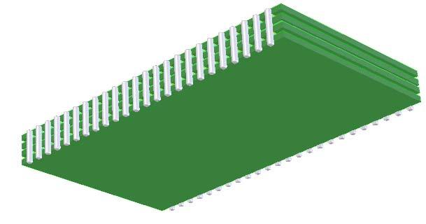
11 Mobile Product Vertical Interconnect Pillar (ViP) mddr mddr Processor mddr Processor Vertical Interconnect Substrate 11


12 VCI Enabled Solid State Drive Continued miniaturization GB VCI Stacked Die WLCSP Engineering SSD Hybrid Drive, 32GB
13 64GB usd (Next Generation Design) 13


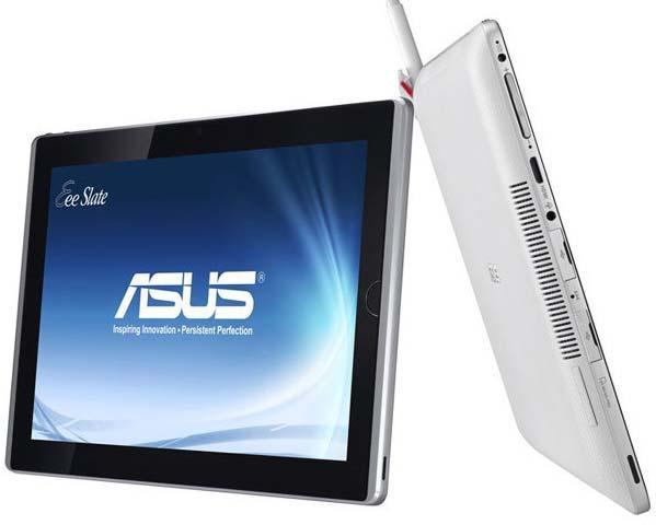

14 SSD Market Focus msata SSD Key Growth Area msata (a small flash module for tablet and Ultra-Portable) Apple Asus Samsung Lenovo 14
15 VCI Markets Solid States Drives Reference Gartner/iSuppli reports SSD adoption continues to grow with projected ~ 60 to 90M SSD in 2012 SSD units CAGR is ~85% In 2012, ~18% of global PC will have SSD installed at POS VCI performance + density solution provide unique value to SSD OEMs 15


16 WLCSP VIP WLCSP ViP Edge WLCSP ViP Foot 16


17 Stackable Leadframe Package 17
 - WiFi / Analog / Bluetooth module package stack - - High density sensor / ASIC MEMS fingerprint, CMOS")
18 Broad Market Applications Vast market potential through broad 3D application - Smallest, highest density memory 8H vertical stack WLCSP - Low power, high speed CPU ASIC SiP (system in package) - WiFi / Analog / Bluetooth module package stack - - High density sensor / ASIC MEMS fingerprint, CMOS sensor 18
19 Technology Summary 19
20 DAG VERTICAL STACK PROCESS FLOW WAFER DIELECTRIC COAT WAFER LASER ABLATION DAF LAMINATION, WAFER MOUNT & BG TAPE REMOVAL WAFER BACKGRIND & POLISH BG TAPE LAMINATION WAFER SCREENPRINT next page 20
21 DAG VERTICAL STACK PROCESS FLOW WAFER DAF TAPE SINGLE- CHANNEL SCRIBE (HALF-CUT DAF) WAFER DAF TAPE 2 ND COAT DICING WAFER DAF TAPE SUBSTRATE VIP & CURE SUBSTRATE DIE STACK WAFER DAF TAPE CODE LASE next page 21


22 DAG VERTICAL STACK PROCESS FLOW MOLD & CURE MARK, SINGULATION & TEST 22

 at fine pitch")

23 VCI Material Selection: Fine Nano Ag Particle Inks Fine line dispense (<40µm) at fine pitch (<65µm) required serial or parallel bus SiP solutions. 23


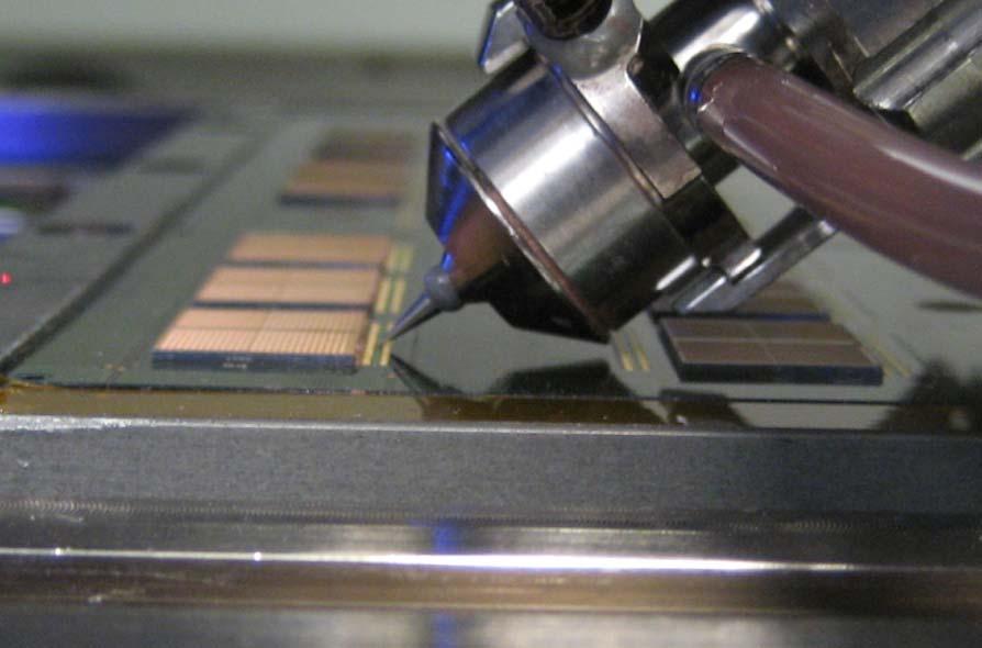
24 Equipment / Material Support HVM Equipment Partnership Creation of HVM system geared toward inkjet printing with high output. 3 separate systems enabling parallel development efforts: a.software b.hardware c.peripherals d.printing capability. Validation of printer settings supplied by VCI and transfer to Q-Class print head. 24 Scanned_printing.MOV

25 Stacking Structures Staggered Edges Aligned Edges Offset Edges 25


26 Vertical Interconnect Structures 100um Conformal Conductors at 200um Pitch on 8-die Stack 16-die NAND Flash Terraced Stack 26 30um Conductors at 200um Pitch on 4-die Stack Arrow Stack with Conformal Interconnect
27 VCI Reliability VCI DRAM (BGA) Server Level Reliability VCI FLASH (µsd) VCI FLASH (LGA) VCI SiP (BGA) Moisture Resist Test: JEDEC Level C JEDEC Level C JEDEC Level C JEDEC Level C Biased HAST: Bias 3.6V, 130 C, 85% RH, 144 hours Bias 3.6V, 130 C, 85% RH, 96 hours Bias 3.6V, 130 C, 85% RH, 96 hours Bias 3.6V, 130 C, 85% RH, 96 hours Autoclave/PCT: Unbiased, 121 C, 2atm, 100%RH, 96 hours NO Unbiased, 121 C, 2atm, 100%RH, 96 hours Unbiased, 121 C, 2atm, 100%RH, 96 hours High Temp Storage: 150 C, 1000 hours 150 C, 1000 hours 150 C, 1000 hours 150 C, 1000 hours Temp Cycle: 55/+125 C, 1000 cycles (B) 55/+125 C, 1000 cycles (B) 55/+125 C, 1000 cycles (B) 55/+125 C, 1000 cycles (B) Card Tests: (DBT/Insert/Salt) N/A SDI Spec. N/A N/A 27 DDR-SDRAM parts tested at Server Level Reliability Specifications. Flash products are simpler and larger, meeting the above specifications for cards and components.

28 Technology Roadmap Trace 1.0mm 2011 key focus: <100um pitch Stagger stack development Embedded ASIC / Controller WLCSP 28
29 KGD A Key Link in The Supply Chain KGD is an enabling building block in the HVM supply chain for multi chip packaging. Is the supply chain getting ahead of KGD? KGD capabilities? KGD costs? Equipment? Operational? Testing does not add value, but is driven by supply chain segmentation. If KGD implementation is too expensive, will other solutions prevail? (eg. Self repair, redundancy) Test cost must be less than yield cost! 29
30 At What Level in the Heirarchy? Interconnect Functional Blocks System Testing Functionality or Construction? Encouraging standards between die suppliers 30
31 Summary 31
32 Summary The Market is Ready! Market applications are demanding multi-die solutions for form factor, functionality, and cost. (Homogeneous & Heterogeneous) Processes are Ready! Multiple solutions to multi die packaging For VCI, Simple Gang/Parallel processing approach facilitates a simple line with reduced logistics and operations, and hence lower cost. Manufacturing Equipment is Ready Some of the Approaches Materials Suppliers are Ready for Some of the Approaches For VCI Conductive Polymers Allow A Near-TSV Edge-Conductor Solution Enabling Chip-Scale Form-Factor Die and Package Stacking. Is KGD ready? Supply chain benefits from KGD infrastructure: Yield & Cost KGD can be an enabler, or an obstacle. If it remains an obstacle, other solutions will prevail. 32
33 THANK YOU 33
Multi-Die Packaging How Ready Are We?
 Multi-Die Packaging How Ready Are We? Rich Rice ASE Group April 23 rd, 2015 Agenda ASE Brief Integration Drivers Multi-Chip Packaging 2.5D / 3D / SiP / SiM Design / Co-Design Challenges: an OSAT Perspective
Advanced Packaging For Mobile and Growth Products
 Advanced Packaging For Mobile and Growth Products Steve Anderson, Senior Director Product and Technology Marketing, STATS ChipPAC Growing Needs for Silicon & Package Integration Packaging Trend Implication
Wafer Level Packaging The Promise Evolves Dr. Thomas Di Stefano Centipede Systems, Inc. IWLPC 2008
 Wafer Level Packaging The Promise Evolves Dr. Thomas Di Stefano Centipede Systems, Inc. IWLPC 2008 / DEVICE 1.E+03 1.E+02 1.E+01 1.E+00 1.E-01 1.E-02 1.E-03 1.E-04 1.E-05 1.E-06 1.E-07 Productivity Gains
Near Term Solutions for 3D Memory Stacking (DRAM) Wael Zohni, Invensas Corporation
 Wael Zohni, Invensas Corporation") Near Term Solutions for 3D Memory Stacking (DRAM) Wael Zohni, Invensas Corporation 1 Contents DRAM Packaging Paradigm Dual-Face-Down (DFD) Package DFD-based 4R 8GB RDIMM Invensas xfd Technology Platform
Near Term Solutions for 3D Memory Stacking (DRAM) Wael Zohni, Invensas Corporation 1 Contents DRAM Packaging Paradigm Dual-Face-Down (DFD) Package DFD-based 4R 8GB RDIMM Invensas xfd Technology Platform
EECS 598: Integrating Emerging Technologies with Computer Architecture. Lecture 10: Three-Dimensional (3D) Integration
 Integration") 1 EECS 598: Integrating Emerging Technologies with Computer Architecture Lecture 10: Three-Dimensional (3D) Integration Instructor: Ron Dreslinski Winter 2016 University of Michigan 1 1 1 Announcements
1 EECS 598: Integrating Emerging Technologies with Computer Architecture Lecture 10: Three-Dimensional (3D) Integration Instructor: Ron Dreslinski Winter 2016 University of Michigan 1 1 1 Announcements
SEMI 大半导体产业网 MEMS Packaging Technology Trend
 MEMS Packaging Technology Trend Authors Name: KC Yee Company Name: ASE Group Present Date:9/9/2010 1 Overview Market Trend Packaging Technology Trend Summary 2 2 MEMS Applications Across 4C Automotive
Company Overview March 12, Company Overview. Tuesday, October 03, 2017
 Company Overview Tuesday, October 03, 2017 HISTORY 1987 2001 2008 2016 Company started to design and manufacture low-cost, highperformance IC packages. Focus on using advanced organic substrates to reduce
3D systems-on-chip. A clever partitioning of circuits to improve area, cost, power and performance. The 3D technology landscape
 Edition April 2017 Semiconductor technology & processing 3D systems-on-chip A clever partitioning of circuits to improve area, cost, power and performance. In recent years, the technology of 3D integration
BRIDGING THE GLOBE WITH INNOVATIVE TECHNOLOGY
 BRIDGING THE GLOBE WITH INNOVATIVE TECHNOLOGY Semiconductor Link Processing & Ultra-Thin Semi Wafer Dicing Louis Vintro VP & General Manager, Semiconductor Products Division Semiconductor Link Processing
Packaging Challenges for High Performance Mixed Signal Products. Caroline Beelen-Hendrikx, Eef Bagerman Semi Networking Day Porto, June 27, 2013
 Packaging Challenges for High Performance Mixed Signal Products Caroline Beelen-Hendrikx, Eef Bagerman Semi Networking Day Porto, June 27, 2013 Content HPMS introduction Assembly technology drivers for
Bringing 3D Integration to Packaging Mainstream
 Bringing 3D Integration to Packaging Mainstream Enabling a Microelectronic World MEPTEC Nov 2012 Choon Lee Technology HQ, Amkor Highlighted TSV in Packaging TSMC reveals plan for 3DIC design based on silicon
Burn-in & Test Socket Workshop
 Burn-in & Test Socket Workshop IEEE March 4-7, 2001 Hilton Mesa Pavilion Hotel Mesa, Arizona IEEE COMPUTER SOCIETY Sponsored By The IEEE Computer Society Test Technology Technical Council COPYRIGHT NOTICE
Packaging Technology for Image-Processing LSI
 Packaging Technology for Image-Processing LSI Yoshiyuki Yoneda Kouichi Nakamura The main function of a semiconductor package is to reliably transmit electric signals from minute electrode pads formed on
TechSearch International, Inc.
 Alternatives on the Road to 3D TSV E. Jan Vardaman President TechSearch International, Inc. www.techsearchinc.com Everyone Wants to Have 3D ICs 3D IC solves interconnect delay problem bandwidth bottleneck
3D & Advanced Packaging
 Tuesday, October 03, 2017 Company Overview March 12, 2015 3D & ADVANCED PACKAGING IS NOW WITHIN REACH WHAT IS NEXT LEVEL INTEGRATION? Next Level Integration blends high density packaging with advanced
Packaging Innovation for our Application Driven World
 Packaging Innovation for our Application Driven World Rich Rice ASE Group March 14 th, 2018 MEPTEC / IMAPS Luncheon Series 1 What We ll Cover Semiconductor Roadmap Drivers Package Development Thrusts Collaboration
Samsung emcp. WLI DDP Package. Samsung Multi-Chip Packages can help reduce the time to market for handheld devices BROCHURE
 Samsung emcp Samsung Multi-Chip Packages can help reduce the time to market for handheld devices WLI DDP Package Deliver innovative portable devices more quickly. Offer higher performance for a rapidly
There is a paradigm shift in semiconductor industry towards 2.5D and 3D integration of heterogeneous parts to build complex systems.
 Direct Connection and Testing of TSV and Microbump Devices using NanoPierce Contactor for 3D-IC Integration There is a paradigm shift in semiconductor industry towards 2.5D and 3D integration of heterogeneous
Innovative 3D Structures Utilizing Wafer Level Fan-Out Technology
 Innovative 3D Structures Utilizing Wafer Level Fan-Out Technology JinYoung Khim #, Curtis Zwenger *, YoonJoo Khim #, SeWoong Cha #, SeungJae Lee #, JinHan Kim # # Amkor Technology Korea 280-8, 2-ga, Sungsu-dong,
High Volume Manufacturing Supply Chain Ecosystem for 2.5D HBM2 ASIC SiPs
 Open-Silicon.com 490 N. McCarthy Blvd, #220 Milpitas, CA 95035 408-240-5700 HQ High Volume Manufacturing Supply Chain Ecosystem for 2.5D HBM2 ASIC SiPs Open-Silicon Asim Salim VP Mfg. Operations 20+ experience
Comparison & highlight on the last 3D TSV technologies trends Romain Fraux
 Comparison & highlight on the last 3D TSV technologies trends Romain Fraux Advanced Packaging & MEMS Project Manager European 3D Summit 18 20 January, 2016 Outline About System Plus Consulting 2015 3D
Advanced Heterogeneous Solutions for System Integration
 Advanced Heterogeneous Solutions for System Integration Kees Joosse Director Sales, Israel TSMC High-Growth Applications Drive Product and Technology Smartphone Cloud Data Center IoT CAGR 12 17 20% 24%
Advancing high performance heterogeneous integration through die stacking
 Advancing high performance heterogeneous integration through die stacking Suresh Ramalingam Senior Director, Advanced Packaging European 3D TSV Summit Jan 22 23, 2013 The First Wave of 3D ICs Perfecting
TechSearch International, Inc.
 Packaging and Assembly for Wearable Electronics Timothy G. Lenihan, Ph.D. Senior Analyst TechSearch International, Inc. www.techsearchinc.com What s Wearable Electronics? Wearable electronics not clearly
3D SYSTEM INTEGRATION TECHNOLOGY CHOICES AND CHALLENGE ERIC BEYNE, ANTONIO LA MANNA
 3D SYSTEM INTEGRATION TECHNOLOGY CHOICES AND CHALLENGE ERIC BEYNE, ANTONIO LA MANNA OUTLINE 3D Application Drivers and Roadmap 3D Stacked-IC Technology 3D System-on-Chip: Fine grain partitioning Conclusion
From 3D Toolbox to 3D Integration: Examples of Successful 3D Applicative Demonstrators N.Sillon. CEA. All rights reserved
 From 3D Toolbox to 3D Integration: Examples of Successful 3D Applicative Demonstrators N.Sillon Agenda Introduction 2,5D: Silicon Interposer 3DIC: Wide I/O Memory-On-Logic 3D Packaging: X-Ray sensor Conclusion
Application Development for Flexible Hybrid Printed Electronics
 Application Development for Flexible Hybrid Printed Electronics Lok Boon Keng, Yusoff Bin Ismail, Joseph Chen Sihan, Cheng Ge, Ronnie Teo Large Area Processing Programme Emerging Application Division Outline
SYSTEM IN PACKAGE AND FUNCTIONAL MODULE FOR MOBILE AND IoT DEVICE ASSEMBLY
 SYSTEM IN PACKAGE AND FUNCTIONAL MODULE FOR MOBILE AND IoT DEVICE ASSEMBLY W. Koh, PhD Huawei Technologies JEDEC Mobile & IOT Forum Copyright 2017 Huawei Technologies, Ltd. OUTLINE Mobile and IoT Device
WLSI Extends Si Processing and Supports Moore s Law. Douglas Yu TSMC R&D,
 WLSI Extends Si Processing and Supports Moore s Law Douglas Yu TSMC R&D, chyu@tsmc.com SiP Summit, Semicon Taiwan, Taipei, Taiwan, Sep. 9 th, 2016 Introduction Moore s Law Challenges Heterogeneous Integration
Challenges of Integration of Complex FHE Systems. Nancy Stoffel GE Global Research
 Challenges of Integration of Complex FHE Systems Nancy Stoffel GE Global Research Products drive requirements to sub-systems, components and electronics GE PRODUCTS CTQs: SWaP, $$, operating environment,
Monolithic 3D Integration using Standard Fab & Standard Transistors. Zvi Or-Bach CEO MonolithIC 3D Inc.
 Monolithic 3D Integration using Standard Fab & Standard Transistors Zvi Or-Bach CEO MonolithIC 3D Inc. 3D Integration Through Silicon Via ( TSV ), Monolithic Increase integration Reduce interconnect total
3D Integration & Packaging Challenges with through-silicon-vias (TSV)
") NSF Workshop 2/02/2012 3D Integration & Packaging Challenges with through-silicon-vias (TSV) Dr John U. Knickerbocker IBM - T.J. Watson Research, New York, USA Substrate IBM Research Acknowledgements IBM
NSF Workshop 2/02/2012 3D Integration & Packaging Challenges with through-silicon-vias (TSV) Dr John U. Knickerbocker IBM - T.J. Watson Research, New York, USA Substrate IBM Research Acknowledgements IBM
LQFP. Thermal Resistance. Body Size (mm) Pkg. 32 ld 7 x 7 5 x ld 7 x 7 5 x ld 14 x 14 8 x ld 20 x x 8.5
 Pkg. 32 ld 7 x 7 5 x ld 7 x 7 5 x ld 14 x 14 8 x ld 20 x x 8.5") LQFP Low Profile Quad Flat Pack Packages (LQFP) Amkor offers a broad line of LQFP IC packages designed to provide the same great benefits as MQFP packaging with a 1.4 mm body thickness. These packages
LQFP Low Profile Quad Flat Pack Packages (LQFP) Amkor offers a broad line of LQFP IC packages designed to provide the same great benefits as MQFP packaging with a 1.4 mm body thickness. These packages
SMAFTI Package Technology Features Wide-Band and Large-Capacity Memory
 SMAFTI Package Technology Features Wide-Band and Large-Capacity Memory KURITA Yoichiro, SOEJIMA Koji, KAWANO Masaya Abstract and NEC Corporation have jointly developed an ultra-compact system-in-package
TABLE OF CONTENTS III. Section 1. Executive Summary
 Section 1. Executive Summary... 1-1 Section 2. Global IC Industry Outlook and Cycles... 2-1 IC Insights' Forecast Methodology... 2-1 Overview... 2-1 Worldwide GDP... 2-1 Electronic System Sales... 2-2
Package (1C) Young Won Lim 3/20/13
 Young Won Lim 3/20/13") Copyright (c) 2011-2013 Young W. Lim. Permission is granted to copy, distribute and/or modify this document under the terms of the GNU Free Documentation License, Version 1.2 or any later version published
Copyright (c) 2011-2013 Young W. Lim. Permission is granted to copy, distribute and/or modify this document under the terms of the GNU Free Documentation License, Version 1.2 or any later version published
TechSearch International, Inc.
 On the Road to 3D ICs: Markets and Solutions E. Jan Vardaman President TechSearch International, Inc. www.techsearchinc.com High future cost of lithography Severe interconnect delay Noted in ITRS roadmap
Advanced CSP & Turnkey Solutions. Fumio Ohyama Tera Probe, Inc.
 Advanced CSP & Turnkey Solutions Fumio Ohyama Tera Probe, Inc. Tera Probe - Corporate Overview 1. Company : Tera Probe, Inc. 2. Founded : August, 2005 3. Capital : Approx. USD118.2 million (as of March
TechSearch International, Inc.
 Silicon Interposers: Ghost of the Past or a New Opportunity? Linda C. Matthew TechSearch International, Inc. www.techsearchinc.com Outline History of Silicon Carriers Thin film on silicon examples Multichip
Package (1C) Young Won Lim 3/13/13
 Young Won Lim 3/13/13") Copyright (c) 2011-2013 Young W. Lim. Permission is granted to copy, distribute and/or modify this document under the terms of the GNU Free Documentation License, Version 1.2 or any later version published
Copyright (c) 2011-2013 Young W. Lim. Permission is granted to copy, distribute and/or modify this document under the terms of the GNU Free Documentation License, Version 1.2 or any later version published
Empowering the Industrial Internet of Things with 3D Printed Sensors and Antennas
 Empowering the Industrial Internet of Things with 3D Printed Sensors and Antennas Agenda! What is the Industrial Internet of Things (IIoT)! Focus on Structural Health Monitoring! Benefits of Structural
Comparison of Singulation Techniques
 Comparison of Singulation Techniques Electronic Packaging Society, Silicon Valley Chapter Sept. 28, 2017 ANNETTE TENG Sept 28, 2017 1 Definition of Singulation 9/28/2017 Annetteteng@promex-ind.com 2 www.cpmt.org/scv
3DIC & TSV interconnects
 3DIC & TSV interconnects 2012 Business update Semicon Taiwan 2012 baron@yole.fr Infineon VTI Xilinx Synopsys Micron CEA LETI 2012 Copyrights Yole Developpement SA. All rights reserved. Semiconductor chip
Introduction. SK hynix
 It was very informative. I had a lot of questions answered. It was a good assembly of design and manufacturing elements. I learned a lot that I didn t know. It s good to hear that TSVs are ready for HBM.
Embedded Power Dies for System-in-Package (SiP)
") Embedded Power Dies for System-in-Package (SiP) D. Manessis, L. Boettcher, S. Karaszkiewicz, R.Patzelt, D. Schuetze, A. Podlasky, A. Ostmann Fraunhofer Institute for Reliability and Microintegration (IZM),
Embedded Power Dies for System-in-Package (SiP) D. Manessis, L. Boettcher, S. Karaszkiewicz, R.Patzelt, D. Schuetze, A. Podlasky, A. Ostmann Fraunhofer Institute for Reliability and Microintegration (IZM),
Emerging IC Packaging Platforms for ICT Systems - MEPTEC, IMAPS and SEMI Bay Area Luncheon Presentation
 Emerging IC Packaging Platforms for ICT Systems - MEPTEC, IMAPS and SEMI Bay Area Luncheon Presentation Dr. Li Li Distinguished Engineer June 28, 2016 Outline Evolution of Internet The Promise of Internet
CMOSETR Session C1, July 7 (Macroelectronics)
") Universal Flexible Hybrid System Development Kit including MCU, ADC and RFIC Prepared for: CMOSETR Session C1, July 7 (Macroelectronics) Doug Hackler President & CEO doughackler@americansemi.com 208 336-2773
Universal Flexible Hybrid System Development Kit including MCU, ADC and RFIC Prepared for: CMOSETR Session C1, July 7 (Macroelectronics) Doug Hackler President & CEO doughackler@americansemi.com 208 336-2773
Dispensing Applications and Methods. August, 2014 Mani Ahmadi, Director of Technical Services Nordson, Advanced Technology Systems
 Dispensing Applications and Methods August, 2014 Mani Ahmadi, Director of Technical Services Nordson, Advanced Technology Systems 1 August 2014 Agenda Introduction Dispensing method and technologies for
Applications, Processing and Integration Options for High Dielectric Constant Multi-Layer Thin-Film Barium Strontium Titanate (BST) Capacitors
 Capacitors") Applications, Processing and Integration Options for High Dielectric Constant Multi-Layer Thin-Film Barium Strontium Titanate (BST) Capacitors Agenda Introduction What is BST? Unique Characteristics of
Applications, Processing and Integration Options for High Dielectric Constant Multi-Layer Thin-Film Barium Strontium Titanate (BST) Capacitors Agenda Introduction What is BST? Unique Characteristics of
Material technology enhances the density and the productivity of the package
 Material technology enhances the density and the productivity of the package May 31, 2018 Toshihisa Nonaka, Ph D. Packaging Solution Center Advanced Performance Materials Business Headquarter Hitachi Chemical
Beyond Chip Stacking---Quilt Packaging Enabled 3D Systems
 Beyond Chip Stacking---Quilt Packaging Enabled 3D Systems Jason Kulick, President & Co-Founder jason.kulick@indianaic.com 574-217-4612 (South Bend, IN) May 3, 2016 2016 New England IMAPS Symposium Presentation
3D technology for Advanced Medical Devices Applications
 3D technology for Advanced Medical Devices Applications By, Dr Pascal Couderc,Jerome Noiray, Dr Christian Val, Dr Nadia Boulay IMAPS MEDICAL WORKSHOP DECEMBER 4 & 5,2012 P.COUDERC 3D technology for Advanced
Interposer Technology: Past, Now, and Future
 Interposer Technology: Past, Now, and Future Shang Y. Hou TSMC 侯上勇 3D TSV: Have We Waited Long Enough? Garrou (2014): A Little More Patience Required for 2.5/3D All things come to those who wait In 2016,
Verification of Singulated HBM2 stacks with Die Level Handler. Dave Armstrong Toshiyuki Kiyokawa Quay Nhin
 Verification of Singulated HBM2 stacks with Die Level Handler Dave Armstrong Toshiyuki Kiyokawa Quay Nhin Abstract Background only will delete on final material High-Bandwidth-Memory continues to evolve
Wafer Probe card solutions
 Wafer Probe card solutions Innovative Solutions to Test Chips in the Semiconductor Industry Our long term experience in the electronic industry and our strong developing and process teams are inspired
E. Jan Vardaman President & Founder TechSearch International, Inc.
 J Wednesday 3/12/14 11:30am Kiva Ballroom TRENDS IN WAFER LEVEL PACKAGING: THIN IS IN! by E. Jan Vardaman President & Founder TechSearch International, Inc. an Vardaman, President and Founder of TechSearch
3-D Package Integration Enabling Technologies
 3-D Package Integration Enabling Technologies Nanium - Semi Networking Day David Clark - Choon Heung Lee - Ron Huemoeller June 27th, 2013 Enabling a Microelectronic World Mobile Communications Driving
The Ascendance of Advanced Packaging: The Future is Now. Byong-Jin Kim I Sr. Director and RD Department Manager, Amkor Technology Malaysia.
 The Ascendance of Advanced Packaging: The Future is Now Byong-Jin Kim I Sr. Director and RD Department Manager, Amkor Technology Malaysia. Market Dynamics Market Trends Package Opportunities Summary Economics
Advances in Flexible Hybrid Electronics Reliability
 Advances in Flexible Hybrid Electronics Reliability LOPEC Smart & Hybrid Systems Munich 3/29/17 This work sponsored in part by Air Force Research Laboratory, Wright-Patterson AFB, for supporting reliability
Product Catalogue
 www.htmicron.com.br Product Catalogue The largest factory of semiconductor packaging and testing in Latin America HT Micron has the most modern factory for semiconductor packaging and testing in Latin
Stacked Silicon Interconnect Technology (SSIT)
") Stacked Silicon Interconnect Technology (SSIT) Suresh Ramalingam Xilinx Inc. MEPTEC, January 12, 2011 Agenda Background and Motivation Stacked Silicon Interconnect Technology Summary Background and Motivation
Stacked Silicon Interconnect Technology (SSIT) Suresh Ramalingam Xilinx Inc. MEPTEC, January 12, 2011 Agenda Background and Motivation Stacked Silicon Interconnect Technology Summary Background and Motivation
Non-contact Test at Advanced Process Nodes
 Chris Sellathamby, J. Hintzke, B. Moore, S. Slupsky Scanimetrics Inc. Non-contact Test at Advanced Process Nodes June 8-11, 8 2008 San Diego, CA USA Overview Advanced CMOS nodes are a challenge for wafer
Moore s Law: Alive and Well. Mark Bohr Intel Senior Fellow
 Moore s Law: Alive and Well Mark Bohr Intel Senior Fellow Intel Scaling Trend 10 10000 1 1000 Micron 0.1 100 nm 0.01 22 nm 14 nm 10 nm 10 0.001 1 1970 1980 1990 2000 2010 2020 2030 Intel Scaling Trend
Solving Integration Challenges for Flexible Hybrid Electronics
 Solving Integration Challenges for Flexible Hybrid Electronics Nano for Defense Conference November 17, 2015 Approved for Public Release What are Flexible Hybrid Electronics? Printed Electronics Low Cost,
Heterogeneous Integration and the Photonics Packaging Roadmap
 Heterogeneous Integration and the Photonics Packaging Roadmap Presented by W. R. Bottoms Packaging Photonics for Speed & Bandwidth The Functions Of A Package Protect the contents from damage Mechanical
Interconnect Challenges in a Many Core Compute Environment. Jerry Bautista, PhD Gen Mgr, New Business Initiatives Intel, Tech and Manuf Grp
 Interconnect Challenges in a Many Core Compute Environment Jerry Bautista, PhD Gen Mgr, New Business Initiatives Intel, Tech and Manuf Grp Agenda Microprocessor general trends Implications Tradeoffs Summary
Power Matters. TM. Why Embedded Die? Piers Tremlett Microsemi 22/9/ Microsemi Corporation. Company Proprietary 1
 Power Matters. TM Why Embedded Die? Piers Tremlett Microsemi 22/9/16 1 Introduction This presentation: Outlines our journey to make miniaturised SiP modules Compares : Embedded Die Technology (EDT) With
Next-Generation Electronic Packaging: Trend & Materials Challenges. Lai Group R&D ASE
 Next-Generation Electronic Packaging: Trend & Materials Challenges Yi-Shao Lai Group R&D ASE Jun 26, 2010 Evolution & Growth of Electronics 2 Evolution of Electronic Products Audion Tube (1906) Transistor
Probing 25µm-diameter micro-bumps for Wide-I/O 3D SICs
 The International Magazine for the Semiconductor Packaging Industry Volume 18, Number 1 January February 2014 Probing 25µm-diameter micro-bumps for Wide-I/O 3D SICs Page 20 3D ICs The future of interposers
SiP Catalyst for Innovation. SWDFT Conference Calvin Cheung ASE Group
 SiP Catalyst for Innovation SWDFT Conference Calvin Cheung ASE Group May 31, 2007 Outline Consumer Electronic Market > Consumer Electronics Market Trends > SiP Drives Innovation > SiP Category SiP - Challenges
ARCHIVE Françoise von Trapp Editorial Director 3D InCites ABSTRACT
 2010 Invited Speaker ARCHIVE 2010 RISING TO THE 3D TSV TEST CHALLENGE: WILL YOU BE READY? by Françoise von Trapp Editorial Director 3D InCites 3D ABSTRACT integration is not a novel concept. Veterans in
An integrated solution for KGD: At-speed wafer-level testing and full-contact wafer-level burn-in after flip chip bumping
 An integrated solution for KGD: At-speed wafer-level testing and full-contact wafer-level burn-in after flip chip bumping Yuan-Ping Tseng/ An-Hong Liu TD center ChipMOS Technologies Inc. June 5, 2001 1
Panel Discussion Chair: Michael Huebner
 Panel Discussion Chair: Michael Huebner FormFactor Inc. Panel members Panel Discussion Mark Ojeda (Spansion/Cypress) Panel: I/II Rey Rincon (Freescale) Panel: II Al Wegleitner (TI) Panel: I/II Clark Liu
Chapter 0 Introduction
 Chapter 0 Introduction Jin-Fu Li Laboratory Department of Electrical Engineering National Central University Jhongli, Taiwan Applications of ICs Consumer Electronics Automotive Electronics Green Power
Case study: Bringing 3D Printed Electronics into Mass Production Lessons Learned
 Case study: Bringing 3D Printed Electronics into Mass Production Lessons Learned Mike O Reilly Optomec, Inc. Henrik Johansson LiteON Mobile Mechanical About Optomec Leader in Printed Electronics and Additive
iphone 5 and iphone 7 (April 14 and 17, 2017) iphone 5 WiFi module iphone 7 battery application processors wafer level packaging 3D NAND
 iphone 5 WiFi module iphone 7 battery application processors wafer level packaging 3D NAND") iphone 5 and iphone 7 (April 14 and 17, 2017) iphone 5 WiFi module iphone 7 battery application processors wafer level packaging 3D NAND 1 iphone 5 2 WiFi Front End in iphone 5 3 Broadcom BCM4334 inside
iphone 5 and iphone 7 (April 14 and 17, 2017) iphone 5 WiFi module iphone 7 battery application processors wafer level packaging 3D NAND 1 iphone 5 2 WiFi Front End in iphone 5 3 Broadcom BCM4334 inside
ARCHIVE 2008 COPYRIGHT NOTICE
 Keynote Speaker ARCHIVE 2008 Packaging & Assembly in Pursuit of Moore s Law and Beyond Karl Johnson Ph.D. Vice President and Senior Fellow Advanced Packaging Systems Integration Laboratory Freescale Semiconductor
Wafer Probe card solutions
 Wafer Probe card solutions Innovative Solutions to Test Chips in the Semiconductor Industry Our long term experience in the electronic industry and our strong developing and process teams are inspired
Shaping Solutions in Advanced Semiconductor Assembly and Test. Pranab Sarma, Product Engineering Manager
 Shaping Solutions in Advanced Semiconductor Assembly and Test Pranab Sarma, Product Engineering Manager STATS ChipPAC Overview 2 What we do total turnkey solutions Wafer design Outsourced Semiconductor
3D-IC is Now Real: Wide-IO is Driving 3D-IC TSV. Samta Bansal and Marc Greenberg, Cadence EDPS Monterey, CA April 5-6, 2012
 3D-IC is Now Real: Wide-IO is Driving 3D-IC TSV Samta Bansal and Marc Greenberg, Cadence EDPS Monterey, CA April 5-6, 2012 What the fuss is all about * Source : ECN Magazine March 2011 * Source : EDN Magazine
Semiconductor Equipment
 Semiconductor Equipment Dept. 81-3-5440-8475 Semiconductor Equipment Mipox Corporation Wafer edge polisher Mipox Edge Polisher has over 140 introduction results to Semiconductor market. G8 用 :2 Bevel shape
TechSearch International, Inc.
 IoT and the Impact on MEMS and Sensors Packaging E. Jan Vardaman President and Founder TechSearch International, Inc. www.techsearchinc.com What is IoT? Internet of Things..Cisco s Internet of Everything
DFT Trends in the More than Moore Era. Stephen Pateras Mentor Graphics
 DFT Trends in the More than Moore Era Stephen Pateras Mentor Graphics steve_pateras@mentor.com Silicon Valley Test Conference 2011 1 Outline Semiconductor Technology Trends DFT in relation to: Increasing
3DIC & TSV interconnects business update
 3DIC & TSV interconnects business update ASET presentation. Infineon VTI Xilinx Synopsys Micron CEA LETI 2012 Copyrights Yole Developpement SA. All rights reserved. Fields of Expertise Yole Developpement
Packaging for parallel optical interconnects with on-chip optical access
 Packaging for parallel optical interconnects with on-chip optical access I. INTRODUCTION Parallel optical interconnects requires the integration of lasers and detectors directly on the CMOS chip. In the
Solving Integration Challenges for Printed and Flexible Hybrid Electronics
 Solving Integration Challenges for Printed and Flexible Hybrid Electronics SEMICON West 16 July 2015 Proprietary Information www.americansemi.com What are Flexible Hybrid Electronics 2 Flexible Hybrid
Ultra Fine Pitch RDL Development in Multi-layer ewlb (embedded Wafer Level BGA) Packages
 Packages") Ultra Fine Pitch RDL Development in Multi-layer ewlb (embedded Wafer Level BGA) Packages Won Kyoung Choi*, Duk Ju Na*, Kyaw Oo Aung*, Andy Yong*, Jaesik Lee**, Urmi Ray**, Riko Radojcic**, Bernard Adams***
Ultra Fine Pitch RDL Development in Multi-layer ewlb (embedded Wafer Level BGA) Packages Won Kyoung Choi*, Duk Ju Na*, Kyaw Oo Aung*, Andy Yong*, Jaesik Lee**, Urmi Ray**, Riko Radojcic**, Bernard Adams***
High performance HBM Known Good Stack Testing
 High performance HBM Known Good Stack Testing FormFactor Teradyne Overview High Bandwidth Memory (HBM) Market and Technology Probing challenges Probe solution Power distribution challenges PDN design Simulation
inemi Roadmap Packaging and Component Substrates TWG
 inemi Roadmap Packaging and Component Substrates TWG TWG Leaders: W. R. Bottoms William Chen Presented by M. Tsuriya Agenda Situation Everywhere in Electronics Evolution & Blooming Drivers Changing inemi
SYSTEM INTEGRATION & PORTABLE/WEARABLE/IOT DEVICES
 AGENDA RECON PACKAGING TECHNOLOGY FOR SYSTEM INTEGRATION & PORTABLE/WEARABLE/IOT DEVICES Edward Law Senior Director Package Engineering, Operations and Central Engineering 1 OUTLINE Market dynamics Connectivity
Business of NAND: Trends, Forecasts & Challenges
 Business of NAND: Trends, Forecasts & Challenges Rahul Advani, Microsemi & Mark Webb, MKW Ventures Key Messages Ramp of 3D NAND will be slower than most people think And uneven by vendor NAND roadmaps
FO-WLP: Drivers for a Disruptive Technology
 FO-WLP: Drivers for a Disruptive Technology Linda Bal, Senior Analyst w w w. t e c h s e a r c h i n c. c o m Outline Industry drivers for IC package volumes WLP products and drivers Fan-in WLP FO-WLP
3D TECHNOLOGIES: SOME PERSPECTIVES FOR MEMORY INTERCONNECT AND CONTROLLER
 3D TECHNOLOGIES: SOME PERSPECTIVES FOR MEMORY INTERCONNECT AND CONTROLLER CODES+ISSS: Special session on memory controllers Taipei, October 10 th 2011 Denis Dutoit, Fabien Clermidy, Pascal Vivet {denis.dutoit@cea.fr}
TSV Test. Marc Loranger Director of Test Technologies Nov 11 th 2009, Seoul Korea
 TSV Test Marc Loranger Director of Test Technologies Nov 11 th 2009, Seoul Korea # Agenda TSV Test Issues Reliability and Burn-in High Frequency Test at Probe (HFTAP) TSV Probing Issues DFT Opportunities
Xilinx SSI Technology Concept to Silicon Development Overview
 Xilinx SSI Technology Concept to Silicon Development Overview Shankar Lakka Aug 27 th, 2012 Agenda Economic Drivers and Technical Challenges Xilinx SSI Technology, Power, Performance SSI Development Overview
SWIR Vision Systems Acuros TM CQD TM SWIR Cameras. November 2018 SWIR VISION SYSTEM
 SWIR Vision Systems Acuros TM CQD TM SWIR Cameras November 2018 SWIR VISION SYSTEM Introducing Quantum Dots for short-wave IR imaging! Acuros TM CQD TM films turn silicon ICs into infrared sensors Encapsulant
PRODUCT Line Card JULY Connecting People & Technology.
 PRODUCT Line Card An Amkor Company Connecting People & Technology JULY 2017 As one of the world s largest suppliers of outsourced semiconductor packaging, design, assembly and test services; Amkor helps
Thermal Management Challenges in Mobile Integrated Systems
 Thermal Management Challenges in Mobile Integrated Systems Ilyas Mohammed March 18, 2013 SEMI-THERM Executive Briefing Thermal Management Market Visions & Strategies, San Jose CA Contents Mobile computing
Bringing a new flexible display technology into mass production. Chuck Milligan CEO, FlexEnable
 Bringing a new flexible display technology into mass production Chuck Milligan CEO, FlexEnable Years of development and investment have made FlexEnable the clear leader in Plastic Large-area Electronics
FHE Integration & Manufacturing for Killer Apps
 FHE Integration & Manufacturing for Killer Apps Nov. 18, 2015 Doug Hackler Introduction Small Business Privately Held Founded Nov. 2001 Member: New Boise, Idaho Facility Headquarters and manufacturing