Unit-IV Peripheral Interfacing S.Sayeekumar, AP/RMDEEE
|
|
|
- Alban Lawson
- 5 years ago
- Views:
Transcription
1 Unit-IV Peripheral Interfacing S.Sayeekumar, AP/RMDEEE
2 8251 The 8251A is a programmable serial communication interface chip designed for synchronous and asynchronous serial data communication. It supports the serial transmission of data. It is packed in a 28 pin DIP.
3 Pin details
4 Architecture
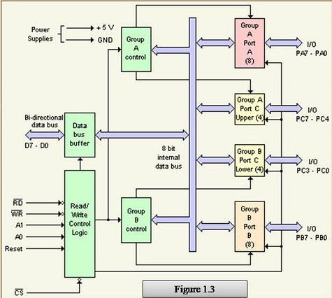
5 Arch - details The functional block diagram of 825 1A consists five sections. They are: Read/Write control logic Transmitter Receiver Data bus buffer Modem control.
6 Read/Write control logic The Read/Write Control logic interfaces the 8251A with CPU, determines the functions of the 8251A according to the control word written into its control register. It monitors the data flow. This section has three registers and they are control register, status register and data buffer. The active low signals RD, WR, CS and C/D(Low) are used for read/write operations with these three registers.
7 Read/Write control logic When C/D(low) is high, the control register is selected for writing control word or reading status word. When C/D(low) is low, the data buffer is selected for read/write operation. When the reset is high, it forces 8251A into the idle mode. The clock input is necessary for 8251A for communication with CPU and this clock does not control either the serial transmission or the reception rate.
8 Transmitter The transmitter section accepts parallel data from CPU and converts them into serial data. The transmitter section is double buffered, i.e., it has a buffer register to hold an 8-bit parallel data and another register called output register to convert the parallel data into serial bits. When output register is empty, the data is transferred from buffer to output register. Now the processor can again load another data in buffer register.
9 Transmitter If buffer register is empty, then TxRDY is goes to high. If output register is empty then TxEMPTY goes to high. The clock signal, TxC (low) controls the rate at which the bits are transmitted by the USART. The clock frequency can be 1,16 or 64 times the baud rate.
10 Receiver The receiver section accepts serial data and convert them into parallel data The receiver section is double buffered, i.e., it has an input register to receive serial data and convert to parallel, and a buffer register to hold the parallel data. When the RxD line goes low, the control logic assumes it as a START bit, waits for half a bit time and samples the line again. If the line is still low, then the input register accepts the following bits, forms a character and loads it into the buffer register.
11 Receiver The CPU reads the parallel data from the buffer register. When the input register loads a parallel data to buffer register, the RxRDY line goes high. The clock signal RxC (low) controls the rate at which bits are received by the USART. During asynchronous mode, the signal SYNDET/BRKDET will indicate the break in the data transmission. During synchronous mode, the signal SYNDET/BRKDET will indicate the reception of synchronous character.
12 Modem control The MODEM control unit allows to interface a MODEM to 8251A and to establish data communication through MODEM over telephone lines. This unit takes care of handshake signals for MODEM interface. The 825 1A can be either memory mapped or I/O mapped in the system. 8251A in I/O mapped in the system is shown in the figure. Using a 3-to-8 decoder generates the chip select signals for I/O mapped devices. The address lines A4, A5 and A6 are decoded to generate eight chip select signals (IOCS-0 to IOCS-7) and in this, the chip select signal IOCS-2 is used to select 8251A. The address line A7 and the control signal IO / M(low) are used as enable for decoder. The address line A0 of 8085 is connected to C/D(low) of 8251A to provide the internal addresses.
13 Modem control The data lines D0 - D7 are connected to D0 - D7 of the processor to achieve parallel data transfer. The RESET and clock signals are supplied by the processor. Here the processor clock is directly connected to 8251A. This clock controls the parallel data transfer between the processor and 8251A. The output clock signal of 8085 is divided by suitable clock dividers like programmable timer 8254 and then used as clock for serial transmission and reception.
14 Modem control The TTL logic levels of the serial data lines and the control signals necessary for serial transmission and reception are converted to RS232 logic levels using MAX232 and then terminated on a standard 9-pin D-.type connector. In 8251A the transmission and reception baud rates can be different or same. The device which requires serial communication with processor can be connected to this 9-pin D-type connector using 9-core cable The signals TxEMPTY, TxRDY and RxRDY can be used as interrupt signals to initiate interrupt driven data transfer scheme between processor and 8251
15 Modem control The CPU reads the parallel data from the buffer register. When the input register loads a parallel data to buffer register, the RxRDY line goes high. The clock signal RxC (low) controls the rate at which bits are received by the USART. During asynchronous mode, the signal SYNDET/BRKDET will indicate the break in the data transmission. During synchronous mode, the signal SYNDET/BRKDET will indicate the reception of synchronous character.
16 8251 mode register Mode register Number of Stop bits 00: invalid 01: 1 bit 10: 1.5 bits 11: 2 bits Parity 0: odd 1: even Parity enable 0: disable 1: enable Character length 00: 5 bits 01: 6 bits 10: 7 bits 11: 8 bits Baud Rate 00: Syn. Mode 01: x1 clock 10: x16 clock 11: x64 clock
17 8251 command register EH IR RTS ER SBRK RxE DTR TxE TxE: transmit enable DTR: data terminal ready RxE: receiver enable SBPRK: send break character ER: error reset RTS: request to send IR: internal reset EH: enter hunt mode
18 8251 status register DSR SYNDET FE OE PE TxEMPTY RxRDY TxRDY TxRDY: RxRDY: TxEMPTY: PE: OE: FE: SYNDET: DSR: transmit ready receiver ready transmitter empty parity error overrun error framing error sync. character detected data set ready
19 8251 interfaced with 8085
20 8255 PPI PPI Programmable Peripheral Interface 20
21 Intel 8255 PPI PPI Programmable Peripheral Interface It is an I/O port chip used for interfacing I/O devices with microprocessor Very commonly used peripheral chip Knowledge of 8255 essential for students in the Microprocessors lab for Interfacing experiments 21
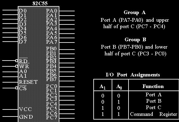
22 About 82C55 The 82C55 is a popular interfacing component, that can interface any TTL-compatible I/O device to a microprocessor. It is used to interface to the keyboard and a parallel printer port in PCs (usually as part of an integrated chipset). Requires insertion of wait states if used with a microprocessor using higher that an 8 MHz clock. PPI has 24 pins for I/O that are programmable in groups of 12 pins and has three distinct modes of operation.

23 82C55 : Pin Layout

24 8255 Control Word

25 Basic Mode Definitions and Bus Int Mode 0 Basic I/O Mode 1 Strobe I/O Mode 2 Bi-Dir Bus


26 Programming has three operation modes: mode 0, mode 1, and mode
27 27
28 8255 PPI contd. 3 ports in 8255 from user s point of view - Port A, Port B and Port C. Port C composed of two independent 4-bit ports - PC7-4 (PC Upper) and PC3-0 (PC Lower) A1 A0 Selected port 0 0 Port A 0 1 Port B 1 0 Port C 1 1 Control port 28
29 Intel 8255 PPI Chip Select Circuit A7 M/IO* U3A U2A U pin DIP V cc (+5V) GND Port A RD PA 7-0 WR PC 7-4 CS Port C PC 3-0 D 7-0 A 1 A 0 Reset Control Port Port B PB 7-0 A7=0, A6=1, A5=1, A4=1, A3=1, A2=1, & M/IO*= 0 29
30 8255 PPI Contd. There is also a Control port from the Processor point of view. Its contents decides the working of When CS (Chip select) is 0, 8255 is selected for communication by the processor. The chip select circuit connected to the CS pin assigns addresses to the ports of For the chip select circuit shown, the chip is selected when A7=0, A6=1, A5=1, A4=1, A3=1, A2=1, & M/IO*= 0 Port A, Port B, Port C and Control port will have the addresses as 7CH, 7DH, 7EH, and 7FH respectively. 30
31 8255 PPI Contd. Mode 0: Simple Input or Output In this mode, ports A, B are used as two simple 8-bit I/O ports port C as two 4-bit ports. Each port can be programmed to function as simply an input port or an output port. The input/output features in Mode 0 are as follows. 1. Outputs are latched. 2. Inputs are not latched. 3. Ports don t have handshake or interrupt capability. 31
32 8255 PPI Contd. Mode 1: Input or Output with Handshake In this mode, handshake signals are exchanged between the MPU and peripherals prior to data transfer. The features of the mode include the following: 1. Two ports (A and B) function as 8-bit I/O ports. They can be configured as either as input or output ports. 2. Each port uses three lines from ort C as handshake signals. The remaining two lines of Port C can be used for simple I/O operations. 3. Input and Output data are latched. 4. Interrupt logic is supported. 32
33 8255 PPI Contd. Mode 2: Bidirectional Data Transfer This mode is used primarily in applications such as data transfer between two computers. In this mode, Port A can be configured as the bidirectional port Port B either in Mode 0 or Mode 1. Port A uses five signals from Port C as handshake signals for data transfer. The remaining three signals from port C can be used either as simple I/O or as handshake for port B. 33
34 8255 Handshake signals Where are the Handshake signals? Port C pins act as handshake signals, when Port A and Port B are configured for other than Mode 0. Port A in Mode 2 and Port B in Mode 1 is possible, as it needs only 5+3 = 8 handshake signals After Reset of 8255, Port A, Port B, and Port C are configured for Mode 0 operation as input ports. 34
35 8255 Handshake signals Contd. PC2-0 are used as handshake signals by Port B when configured in Mode 1. This is immaterial whether Port B is configured as i/p or o/p port. PC5-3 are used as handshake signals by Port A when configured as i/p port in Mode 1. PC7,6,3 are used as handshake signals by Port A when configured as o/p port in Mode 1. PC7-3 are used as handshake signals by Port A when configured in Mode 2. 35
36 8255 PPI Contd. Port A can work in Mode 0, Mode 1, or Mode 2 Port B can work in Mode 0, or Mode 1 Port C can work in Mode 0 only, if at all Port A, Port B and Port C can work in Mode 0 Port A and Port B can work in Mode 1 Only Port A can work in Mode 2 36
37 8255 MD Control word Control port having Mode Definition (MD) control word 1 M2A M1A I/P A I/P C U M1B I/P B I/P C L Means Mode Definition control word M2A M1A 1 - PC U as input 0 - PC U as output 1 - PA as input 0 - PA as output 0 0 Port A in Mode Port A in Mode 1 1 0/1 Port A in Mode 2 1 -PC L as input 0 -PC L as output 1 - PB as input 0 - PB as output 1 Port B in Mode 1 0 Port B in Mode 0 37
38 8255 MD Control word Contd. Ex. 1: Configure Port A as i/p in Mode 0, Port B as o/p in mode 0, Port C (Lower) as o/p and Port C (Upper) as i/p ports. Required MD control word: MD control = 98H PA in Mode 0 PA as i/p PC Lower as o/p PB as o/p Reqd. instrns. PB in Mode 0 MOV AL, 98H PC Upper as i/p OUT 7FH, AL 38
39 8255 MD Control word Contd. Ex. 2: Configure Port A as i/p in Mode 1, Port B as o/p in mode 1, Port C7-8 as i/p ports. (PC5-0 are handshake lines, some i/p lines and others o/p. So they are shown as X) Required MD control word: MD control X = BCH or BDH PA in Mode 1 PA as i/p PC3-0 as don t care PB as o/p Reqd. Instrns. PB in Mode 1 MOV AL,BCH PC Upper(C7-8) as i/p OUT 7FH, AL 39
40 8255 Contd. There are 2 control words in 8255 Mode Definition (MD) Control word and Port C Bit Set / Reset (PCBSR) Control Word MD control word configures the ports of as i/p or o/p in Mode 0, 1, or 2 PCBSR control word is used to set to 1 or reset to 0 any one selected bit of Port C 40
41 8255 MD Control word Contd. Ex. 3:Configure Port A in Mode 2, Port B as o/p in mode 1. (PC5-0 are handshake lines for Port A and PC2-0 are handshake signals for port B) Required MD control word: MD control X X 1 0 X = C4H / C5H.. PA in Mode 2 PA bidirectional PC3-0 as handshake PB as o/p Reqd. instrns. PB in Mode 1 MOV AL, C4H PC7-0 as handshake OUT 7FH, AL 41
42 8255 PCBSR Control word Control port having Port C Bit Set / Reset control word PC bit set / reset control word 0 X X X SB2 SB1 SB0 S/R* Don t Select bit of PC to be set / reset 1 - Set to Reset to 0 cares Bit 0 of Port C Bit 1 of Port C : : Bit 7 of Port C 42
43 8253 / 8254 Timer To program a given counter to divide the CLK input frequency, one must send the divisor to that specific counter s register. Although all three counters share the same control register, the divisor registers are separate for each counter Example: given the port addresses for 8253/54: Counter 0: 94H Counter 1: 95H Counter 2: 96H Control Reg: 97H Engr 4862 Microprocessors
44 8253 / 8254 Timer Task1: program counter 0 for binary counter for mode 3 to divide CLK0 by number 4282 (BCD) MOV AL, B OUT 97H, AL MOV AX, 4282H (BCD needs H) OUT 94H, AL (Low Byte) MOV AL, AH OUT 94H, AL (High Byte) OUT0 = CLK0 / 4282 Engr 4862 Microprocessors
45 Shape of the 8253/54 Output Given CLK = MHz, the clock period of input frequency is 838 ns If the number N loaded into the counter is even, both high and low pulse are the same length, which is N/2 * 838 ns If the number N loaded into the counter is odd, the high pulse is (N+1)/2 * 838 ns and the low pulse is (N 1)/2 * 838 ns If N is odd, the high portion of the output square wave is slightly wider than the low portion Engr 4862 Microprocessors
46 8253/54 Operation Modes Mode 0: Interrupt on terminal count The output is initially low, and remain low for the duration of the count if GATE=1. When the terminal count is reached, the output will go high and remain high until a new control word or new count number is loaded Width of low pulse = N * T, where T is clock period Example: GATE=1 and CLK = 1 MHz Clock count N = 1000 Engr 4862 Microprocessors
47 8253/54 Operation Modes Mode 0: Interrupt on terminal count If GATE becomes low at the middle of the count, the count will stop and the output will be low. The count resumes when the GATE becomes high again This in effect adds to the total time the output is low. Mode 1: HW triggered / programmable one shot The triggering must be done through the GATE input by sending a 0-to-1 pulse to it. Steps: 1) Load the count register GATE 2) A 0-to-1 Engr 4862 pulse Microprocessors must be sent to the input to trigger the count
48 8253/54 Operation Modes Mode 1: HW triggered / programmable one shot In Mode 1, after sending the 0-to-1 pulse to GATE, OUT becomes low and stays low for a duration of N*T, then becomes high and stays high until the GATE is triggered again If during the activation, a retriggered happened, then restart the down counting Mode 2: Rate Generator (Divide-by-N counter) In Mode2, if GATE=1, OUT will be high for N*T, goes low only for one clock pulse, then counter is Engr 4862 Microprocessors reloaded automatically, and the process
49 8253/54 Operation Modes Mode 3: Square wave rate generator Most commonly used Mode 4: Software triggered strobe Similar to Mode2, except that the counter is not reloaded automatically In Mode4, if GATE=1, the output will go high when loading the count, it will stay high for duration N*T. After the count reaches zero, it becomes low for one clock pulse, then goes high again and stays high until a new command word or new count is loaded To repeat the strobe, the count must be reloaded Engr 4862 Microprocessors
50 8253/54 Operation Modes Mode 5: Hardware triggered strobe Similar to Mode4, except that the triggering must be done with the GATE input The count starts only when a 0-to-1 pulse is sent to the GATE input If GATE retriggered during the counting, it will restart the down counting Engr 4862 Microprocessors

51 8253 / 8254 Timer Engr 4862 Microprocessors
52 8253 / 8254 Timer Engr 4862 Microprocessors

53 8253 / 8254 Timer Engr 4862 Microprocessors

54 8253 / 8254 Timer Engr 4862 Microprocessors

55 8253 / 8254 Timer Engr 4862 Microprocessors

56 8253 / 8254 Timer Engr 4862 Microprocessors

57 8253 / 8254 Timer Engr 4862 Microprocessors

58 8253 / 8254 Timer Engr 4862 Microprocessors

59 8253 / 8254 Timer Engr 4862 Microprocessors
60 is Programmable Interrupt Controller (PIC) It is a tool for managing the interrupt requests is a very flexible peripheral controller chip:pic can deal with up to 64 interrupt inputs interrupts can be masked various priority schemes can also programmed. originally (in PC XT) it is available as a separate IC Later the functionality of (two PICs) is in the motherboards chipset.
61 Pin description 8-bit bi-directional data bus, one address line is needed,the direction of data flow is controlled by RD and WR. CS is as usual connected to the output of the address decoder. Interrupt requests are output on INT which is connected to the INTR of the processor. Int. acknowledgment is received by INTA. IR0-IR7 allow 8 separate interrupt requests to be inputted to the PIC. sp/en=1 for master, sp/en=0 for slave. CAS0-3 inputs/outputs are used when more than one PIC to cascaded.
62 FIGURE 9-4 Corporation.) Block diagram and pin definitions for the 8259A Programmable Interrupt Controller (PIC). (Courtesy of Intel
63 FIGURE 9-5 Interfacing the PIC to the 386 and 486 processors. Two I/O ports are required.
64 FIGURE 9-7 All interrupt requests must pass through the PIC s interrupt request register (IRR) and interrupt mask register (IMR). If put in service, the appropriate bit of the in-service (IS) register is set.
65 Example of two cascaded PICs
66 OPERATION PIC is to be initialized and programmed to control its operation. The operation in simple words: When an interrupt occurs, the PIC determines the highest priority, activates the processor via its INTR input, and sends the type number onto the data bus when the processor acknowledges the interrupt. Priority: What is used in PC is fully nested mode. That is the lowest numbered IRQ input has highest priority. Lower priority interrupts will not be forwarded to the processor until the higher priority interrupts have been serviced.
67 FIGURE 9-8 (a) Simultaneous interrupt requests arrive on IR4 and IR6. IR4 has highest priority and its IS bit is set as the IR4 service routine is put in service. (b) The IR4 service routine issues a rotate-on-nonspecific-eoi command, resetting IS4 and assigning it lowest priority. IR6 is now placed in service. (c) The IR6 service routine issues a rotate-on-nonspecific-eoi command, resetting IS6 and assigning it lowest priority. John Uffenbeck The 80x86 Family: Design, Programming, and Interfacing, 3e Copyright 2002 by Pearson Education, Inc. Upper Saddle River, New Jersey All rights reserved.
68 FIGURE 9-9 Example illustrating the difference between the rotate-on-nonspecific-eoi command and the rotate-on-specific- EOI command.
69 Modes Fully Nested mode Special Fully Nested mode Nonspecific Rotating Specific Rotating Special Mask Polling
70 FIGURE A initialization control word format. (Courtesy of Intel Corporation.) John Uffenbeck The 80x86 Family: Design, Programming, and Interfacing, 3e Copyright 2002 by Pearson Education, Inc. Upper Saddle River, New Jersey All rights reserved.
71 Features of 8279 The important features of 8279 are, Simultaneous keyboard and display operations. Scanned keyboard mode. Scanned sensor mode. 8-character keyboard FIFO. 1 6-character display. Right or left entry 1 6-byte display RAM. Programmable scan timing.
72 Pin details A0: Selects data (0) or control/status (1) for reads and writes between micro and Output that blanks the displays. CLK: Used internally for timing. Max is 3 MHz. CN/ST: Control/strobe, connected to the control key on the keyboard. Chip select that enables programming, reading the keyboard, etc. DB7-DB0: Consists of bi-directional pins that connect to data bus on micro.

73 Pin details IRQ: Interrupt request, becomes 1 when a key is pressed, data is available. OUT A3-A0/B3-B0: Outputs that sends data to the most significant/least significant nibble of display. : Connects to micro's IORC or RD signal, reads data/status registers. RESET: Connects to system RESET. RL7-RL0: Return lines are inputs used to sense key depression in the keyboard matrix. Shift: Shift connects to Shift key on keyboard. SL3-SL0: Scan line outputs scan both the keyboard and displays.
74 Block diagram of 8279
75 Sections Keyboard Display Scan CPU interface
76 Keyboard section The keyboard section consists of eight return lines RL0 - RL7 that can be used to form the columns of a keyboard matrix. It has two additional input : shift and control/strobe. The keys are automatically debounced. The two operating modes of keyboard section are 2-key lockout and N-key rollover. In the 2-key lockout mode, if two keys are pressed simultaneously, only the first key is recognized. In the N-key rollover mode simultaneous keys are recognized and their codes are stored in FIFO. The keyboard section also have an 8 x 8 FIFO (First In First Out) RAM. The FIFO can store eight key codes in the scan keyboard mode. The status of the shift key and control key are also stored along with key code. The 8279 generate an interrupt signal when there is an entry in FIFO.
77 Display section The display section has eight output lines divided into two groups A0-A3 and B0-B3. The output lines can be used either as a single group of eight lines or as two groups of four lines, in conjunction with the scan lines for a multiplexed display. The output lines are connected to the anodes through driver transistor in case of common cathode 7-segment LEDs. The cathodes are connected to scan lines through driver transistors. The display can be blanked by BD (low) line. The display section consists of 16 x 8 display RAM. The CPU can read from or write into any location of the display RAM.
78 Scan section The scan section has a scan counter and four scan lines, SL0 to SL3. In decoded scan mode, the output of scan lines will be similar to a 2-to-4 decoder. In encoded scan mode, the output of scan lines will be binary count, and so an external decoder should be used to convert the binary count to decoded output. The scan lines are common for keyboard and display. The scan lines are used to form the rows of a matrix keyboard and also connected to digit drivers of a multiplexed display, to turn ON/OFF.
79 CPU interface section The CPU interface section takes care of data transfer between 8279 and the processor. This section has eight bidirectional data lines DB0 to DB7 for data transfer between 8279 and CPU. It requires two internal address A =0 for selecting data buffer and A = 1 for selecting control register of8279. The control signals WR (low), RD (low), CS (low) and A0 are used for read/write to It has an interrupt request line IRQ, for interrupt driven data transfer with processor. The 8279 require an internal clock frequency of 100 khz. This can be obtained by dividing the input clock by an internal prescaler. The RESET signal sets the 8279 in 16-character display with two -key lockout keyboard modes.

80 Control Word Description: First three bits given below select one of 8 control registers (opcode). 000DDMMM Mode set: Opcode 000. DD sets displays mode. MMM sets keyboard mode. DD field selects either: 8- or 16-digit display Whether new data are entered to the rightmost or leftmost display position.
.")
81 Control Word Description: MMM field: MMM Encoded Mode: SL outputs are active-high, follow binary bit pattern 0-7 or 0-15 depending on 8 or 16 digit display. Decoded Mode: SL outputs are active-low (only one of the four outputs will be low at any time).pattern output: 1110, 1101, 1011, 0111.
82 Control Word Description: I/O Interface Strobe : An active high pulse on the CN/ST input pin strobes data from the RL pins into an internal FIFO for reading by micro later. 2-key lockout/n-key rollover: Prevents 2 keys from being recognized if pressed simultaneously/accepts all keys pressed from 1st to last.
83 Write display format 100ZAAAA write display Selects address to write address of one of the Display. Z selects auto-increment so subsequent writes go to subsequent display positions.
84 Clear Display format 1100CCFA The clear control word clears the display, FIFO or both Bit F clears FIFO and the display RAM status, and sets address pointer to 000. If CC are 00 or 01, all display RAM locations become If CC is 10, --> , if CC is 11, -->
85
86 Basic DMA concept Direct memory access (DMA) is a feature of modern computer systems that allows certain hardware subsystems to read/write data to/from memory without microprocessor intervention, allowing the processor to do other work. Used in disk controllers, video/sound cards etc, or between memory locations. Typically, the CPU initiates DMA transfer, does other operations while the transfer is in progress, and receives an interrupt from the DMA controller once the operation is complete. Can create cache coherency problems (the data in the cache may be different from the data in the external memory after DMA) 86
87 The 8237 DMA controller Supplies memory and I/O with control signals and addresses during DMA transfer 4-channels (expandable) 0: DRAM refresh 1: Free 2: Floppy disk controller 3: Free 1.6MByte/sec transfer rate 64 KByte section of memory address capability with single programming fly-by controller (data does not pass through the DMA-only memory to I/O transfer capability) Initialization involves writing into each channel: i) The address of the first byte of the block of data that must be transferred (called the base address). ii) The number of bytes to be transferred (called the word count). 87
88 8237 pins CLK: System clock CS : Chip select (decoder output) RESET: Clears registers, sets mask register READY: 0 for inserting wait states HLDA: Signals that the μp has relinquished buses DREQ3 DREQ0: DMA request input for each channel DB7-DB0: Data bus pins IOR : Bidirectional pin used during programming and during a DMA write cycle IOW : Bidirectional pin used during programming and during a DMA read cycle EOP : End of process is a bidirectional signal used as input to terminate a DMA process or as output to signal the end of the DMA transfer A3-A0: Address pins for selecting internal registers A7-A4: Outputs that provide part of the DMA transfer address HRQ: DMA request output DACK3-DACK0: DMA acknowledge for each channel. AEN: Address enable signal ADSTB: Address strobe MEMR : Memory read output used in DMA read cycle MEMW : Memory write output used in DMA write cycle 88
89 8237 pin Diagram 89
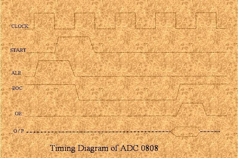
90 A 8237 DMA application DMA ARCHITECTURE 90
91 8237 registers CAR (Current Address Register): holds the 16-bit memory address used for the DMA transfer (one for each channel), either incremented or decremented during the operation CWCR (Current Word Count Register): Programs a channel for the number of bytes (up to 64K) transferred during a DMA operation BA (Base Address) and WC (Word Count): Used when auto-initialization is selected for a channel, to reload the CAR and CWCR when DMA is complete. CR (Command Register): Programs the operation of the controller 91
92 MR (Mode Register): Programs the mode of operation for a channel (one for each channel). 92
93 MR (Mask Register): SR (Status Register): Shows the status of each DMA channel 93
94 8237 Software commands 94
95 8237 Software commands Clear First/Last Flip-Flop - This command is executed prior to writing or reading new address or word count information to the 82C37. This command initializes the flipflop to a known state (low byte first) so that subsequent accesses to register contents by the microprocessor will address upper and lower bytes in the correct sequence. Set First/Last Flip-Flop - This command will set the flip-flop to select the high byte first on read and write operations to address and word count registers. Master Clear - This software instruction has the same effect as the hardware Reset. The Command, Status, Request, and Temporary registers, and Internal First/Last Flip-Flop and mode register counter are cleared and the Mask register is set. The 82C37A will enter the idle cycle. Clear Mask Register - This command clears the mask bits of all four channels, enabling them to accept DMA requests. Clear Mode Register Counter - Since only one address location is available for reading the Mode registers, an internal two-bit counter has been included to select Mode registers during read operation. To read the Mode registers, first execute the Clear Mode Register Counter command, then do consecutive reads until the desired channel is read. Read order is channel 0 first, channel 3 last. The lower two bits on all Mode registers will read as ones. 95
96 8237 block diagram 96
97 Initiating a DMA transaction Save the current interrupt status and disable interrupts by executing the CLI instruction Disable the channel that will be used for the transaction Reset the flip-flop by writing a value of 0X to the register Set the Mode Register Set the Page Register Set the Offset Register Set the Block Size Register Enable the channel that will be used for the transaction Restore the interrupt status 97
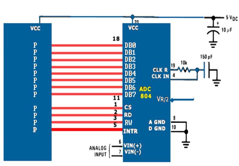
98 A/D Interfacing After the conversion is over, the ADC sends end of conversion EOC signal to inform the microprocessor that the conversion is over and the result is ready at the output buffer of the ADC. These tasks of issuing an SOC pulse to ADC, reading EOC signal from the ADC and reading the digital output of the ADC are carried out by the CPU using 8255 I/O ports.
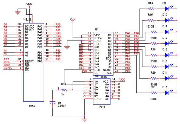
99 A/D Interfacing The time taken by the ADC from the active edge of SOC pulse till the active edge of EOC signal is called as the conversion delay of the ADC. Successive approximation techniques and dual slope integration techniques are the most popular techniques used in the integrated ADC chip. The analog to digital converter chips 0808 and 0809 are 8-bit CMOS, successive approximation converters.
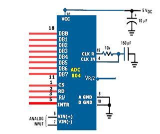
100 ADC 0804
101 ADC Interfacing CS :Active low input used to activate the ADC0804 chip. RD (data enable) : Active low input used to get converted data out of the ADC0804 chip. When CS = 0, if a high-to-low pulse is applied to the RD pin, the 8-bit digital output shows up at the D0-D7 data pins. WR (start conversion): Active low input used to inform the ADC0804 to start the conversion process. If CS = 0 when WR makes a low-to-high transition, the ADC0804 starts converting the analog input value of Vin to an 8-bit digital number. When the data conversion is complete, the INTR pin is forced low by the ADC0804.
102 ADC Interfacing CLK IN and CLK R : Connect to external capacitor and resistor for self-clocking, f = 1/(1.1RC). The clock affect the conversion time and this time cannot be faster than 110 micros. INTR (end of conversion) This is an active low output pin. When the conversion is finished, it goes low to signal the CPU that the converted data is ready to be picked up. After INTR goes low, we make CS = 0 and send a high-to-low pulse to the RD pin to get the data out of the ADC0804 chip.
103 ADC Interfacing Vin (+) and Vin (-) :These are the differential analog inputs where Vin = Vin (+) - Vin (-). Often the Vin (-) pin is connected to ground and the Vin (+) pin is used as the analog input to be converted to digital. VCC : This is the +5V power supply. It is also used as a reference voltage when the Vref/2 (pin 9) input is open.
104 ADC Interfacing Vref/2 :- Input voltage pin used for the reference voltage. If this pin is open, the analog input voltage for the the ADC is ranged from 0 to 5 volts.this is optional input pin. It is used only when the input signal range is small. When pin 9 is at 2V, the range is 0-4V, i.e. Twice the voltage at pin 9. Pin 6 (V+), Pin 7(V-): The actual input is the difference in voltages applied to these pins. The analogue input can range from 0 to 5V.
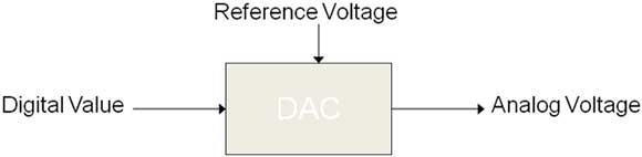
105 ADC Interfacing
106 ADC Interfacing
107 A/D Interfacing [0808 ]

108 A/D Interfacing The ADC 0808 is 8-channel 8-bit ADC chip. It has 8 analog inputs i.e. IN0-IN7.
109 A/D Interfacing
110 A/D Interfacing
111 A/D Interfacing
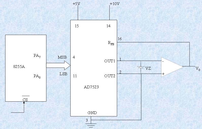
112 3/9/14 D/A INTERFACING DEEPAK.P

113 D/A Interfacing The digital to analog converters convert binary number into their equivalent voltages. The DAC find applications in areas like digitally controlled gains, motors speed controls, programmable gain amplifiers etc.
114 D/A Interfacing
115 D/A Interfacing
116 D/A Interfacing
117 D/A Interfacing
118 D/A Interfacing
119 D/A Interfacing
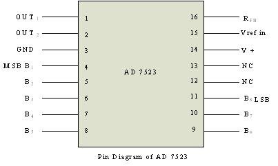
120 D/A Interfacing AD bit Multiplying DAC : This is a 16 pin DIP, multiplying digital to analog converter, containing R-2R ladder for D-A conversion along with single pole double thrown NMOS switches to connect the digital inputs to the ladder. supply range is from +5V to +15V, while Vref may be any where between -10V to +10V. The maximum analog output voltage will be any where between - 10V to +10V, when all the digital inputs are at logic high state.
121 D/A Interfacing
122 D/A Interfacing
123 D/A Interfacing
124 D/A Interfacing
UNIT - II PERIPHERAL INTERFACING WITH 8085
 UNIT - II PERIPHERAL INTERFACING WITH 8085 Peripheral Interfacing is considered to be a main part of Microprocessor, as it is the only way to interact with the external world. The interfacing happens with
Topics. Interfacing chips
 8086 Interfacing ICs 2 Topics Interfacing chips Programmable Communication Interface PCI (8251) Programmable Interval Timer (8253) Programmable Peripheral Interfacing - PPI (8255) Programmable DMA controller
MAHALAKSHMI ENGINEERING COLLEGE TIRUCHIRAPALLI UNIT IV I/O INTERFACING PART A (2 Marks)
") MAHALAKSHMI ENGINEERING COLLEGE TIRUCHIRAPALLI-621213. UNIT IV I/O INTERFACING PART A (2 Marks) 1. Name the three modes used by the DMA processor to transfer data? [NOV/DEC 2006] Signal transfer mode (cycling
MAHALAKSHMI ENGINEERING COLLEGE TIRUCHIRAPALLI-621213. UNIT IV I/O INTERFACING PART A (2 Marks) 1. Name the three modes used by the DMA processor to transfer data? [NOV/DEC 2006] Signal transfer mode (cycling
Intel 8255 PPI. Presented By: Diwakar Yagyasen Asst. Prof. CSE BBDNITM, Lucknow.
 Intel 8255 PPI Presented By: Diwakar Yagyasen Asst. Prof. CSE BBDNITM, Lucknow. 8255 PPI PPI: Programmable Peripheral Interface 2 Intel 8255 PPI PPI Programmable Peripheral Interface It is an I/O port
Chapter 13 Direct Memory Access and DMA-Controlled I/O
 Chapter 13 Direct Memory Access and DMA-Controlled I/O The DMA I/O technique provides direct access to the memory while the microprocessor is temporarily disabled This allows data to be transferred between
Interface DAC to a PC. Control Word of MC1480 DAC (or DAC 808) 8255 Design Example. Engineering 4862 Microprocessors
 8255 Design Example. Engineering 4862 Microprocessors") Interface DAC to a PC Engineering 4862 Microprocessors Lecture 22 Cheng Li EN-4012 licheng@engr.mun.ca DAC (Digital-to-Analog Converter) Device used to convert digital pulses to analog signals Two methods
Interface DAC to a PC Engineering 4862 Microprocessors Lecture 22 Cheng Li EN-4012 licheng@engr.mun.ca DAC (Digital-to-Analog Converter) Device used to convert digital pulses to analog signals Two methods
9. PERIPHERAL CHIPS 9a
 9. PERIPHERAL CHIPS 9a 8255: Programmable Peripheral Interface. Draw the pin diagram of PPI 8255. Ans. The pin diagram of 8255 is shown in Fig. 9a. PA 3 4 PA 4 PA2 2 39 PA 5 PA 3 38 PA 6 PA 4 37 PA7 RD
EC2304-MICROPROCESSOR AND MICROCONROLLERS 2 marks questions and answers UNIT-I
 EC2304-MICROPROCESSOR AND MICROCONROLLERS 2 marks questions and answers 1. Define microprocessors? UNIT-I A semiconductor device(integrated circuit) manufactured by using the LSI technique. It includes
Hierarchy of I/O Control Devices
 Hierarchy of I/O Control Devices 8155 I/O + Timer 2 Port (A,B), No Bidirectional HS mode (C) 4 mode timer 8253/54 Timer 6 mode timer 8255 I/O 2 Port (A,B) A is Bidirectional HS mode (C) Extra controls
The 8237 DMA Controller: -
 The 8237 DMA Controller: - The 8237 is the LSI controller IC that is widely used to implement the direct memory access (DMA) function in 8088 and 8086 based microcomputer systems. It is available in 40-pin
Features: 3 8-bit IO ports PA, PB, PC. PA can be set for Modes 0, 1, 2. PB for 0,1 and PC for mode 0 and for BSR. Modes 1 and 2 are interrupt driven.
 Features: 3 8-bit IO ports PA, PB, PC PA can be set for Modes, 1, 2. PB for,1 and PC for mode and for BSR. Modes 1 and 2 are interrupt driven. PC has 2 4-bit parts: PC upper (PCU) and PC lower (PCL), each
This set of Microprocessor Multiple Choice Questions & Answers (MCQs) focuses on PIO 8255 (Programmable Input Output Port).
 focuses on PIO 8255 (Programmable Input Output Port).") This set of Microprocessor Multiple Choice Questions & Answers (MCQs) focuses on PIO 8255 (Programmable Input Output Port). 1. Programmable peripheral input-output port is other name for a) serial input-output
This set of Microprocessor Multiple Choice Questions & Answers (MCQs) focuses on PIO 8255 (Programmable Input Output Port). 1. Programmable peripheral input-output port is other name for a) serial input-output
These three counters can be programmed for either binary or BCD count.
 S5 KTU 1 PROGRAMMABLE TIMER 8254/8253 The Intel 8253 and 8254 are Programmable Interval Timers (PTIs) designed for microprocessors to perform timing and counting functions using three 16-bit registers.
Design with Microprocessors
 Design with Microprocessors Year III Computer Science 1-st Semester Lecture 11: I/O transfer with x86 I/O Transfer I/O Instructions We discussed IN, OUT, INS and OUTS as instructions for the transfer of
Unit DMA CONTROLLER 8257
 DMA CONTROLLER 8257 In microprocessor based system, data transfer can be controlled by either software or hardware. To transfer data microprocessor has to do the following tasks: Fetch the instruction
Question Bank Microprocessor and Microcontroller
 QUESTION BANK - 2 PART A 1. What is cycle stealing? (K1-CO3) During any given bus cycle, one of the system components connected to the system bus is given control of the bus. This component is said to
Pin Description, Status & Control Signals of 8085 Microprocessor
 Pin Description, Status & Control Signals of 8085 Microprocessor 1 Intel 8085 CPU Block Diagram 2 The 8085 Block Diagram Registers hold temporary data. Instruction register (IR) holds the currently executing
AE66/AC66/AT66/ AE108/AC108/AT108 MICROPROCESSORS & MICROCONTROLLERS
 Q.2 a. Draw pin diagram and signal group diagram of 8085 microprocessor. (8) b. List out the various categories of the 8085 instructions. Give examples of the instructions for each group. (8) Data transfer
UNIT-IV. The semiconductor memories are organized as two-dimensional arrays of memory locations.
 UNIT-IV MEMORY INTERFACING WITH 8086: The semi conductor memories are of two types: Static RAM Dynamic RAM The semiconductor memories are organized as two-dimensional arrays of memory locations. For Ex:
Chapter 1: Basics of Microprocessor [08 M]
![Chapter 1: Basics of Microprocessor [08 M]](/thumbs/77/75860546.jpg "Chapter 1: Basics of Microprocessor [08 M]") Microprocessor: Chapter 1: Basics of Microprocessor [08 M] It is a semiconductor device consisting of electronic logic circuits manufactured by using either a Large scale (LSI) or Very Large Scale (VLSI)
Microprocessor: Chapter 1: Basics of Microprocessor [08 M] It is a semiconductor device consisting of electronic logic circuits manufactured by using either a Large scale (LSI) or Very Large Scale (VLSI)
Week 11 Programmable Interrupt Controller
 Week 11 Programmable Interrupt Controller 8259 Programmable Interrupt Controller The 8259 programmable interrupt controller (PIC) adds eight vectored priority encoded interrupts to the microprocessor.
8254 is a programmable interval timer. Which is widely used in clock driven digital circuits. with out timer there will not be proper synchronization
 8254 is a programmable interval timer. Which is widely used in clock driven digital circuits. with out timer there will not be proper synchronization between two devices. So it is very useful chip. The
7/19/2013. Introduction. Chapter Objectives Upon completion of this chapter, you will be able to: Chapter Objectives 12 1 BASIC INTERRUPT PROCESSING
 Chapter 12: Interrupts Introduction In this chapter, the coverage of basic I/O and programmable peripheral interfaces is expanded by examining a technique called interrupt-processed I/O. An interrupt is
Chapter 12: Interrupts
 Chapter 12: Interrupts Introduction In this chapter, the coverage of basic I/O and programmable peripheral interfaces is expanded by examining a technique called interrupt-processed I/O. An interrupt is
2. List the five interrupt pins available in INTR, TRAP, RST 7.5, RST 6.5, RST 5.5.
 DHANALAKSHMI COLLEGE OF ENGINEERING DEPARTMENT OF ELECTRICAL AND ELECTRONICS ENGINEERING EE6502- MICROPROCESSORS AND MICROCONTROLLERS UNIT I: 8085 PROCESSOR PART A 1. What is the need for ALE signal in
PROGRAMMABLE PERIPHERAL INTERFACE (PPI) -8255
 -8255") PROGRAMMABLE PERIPHERAL INTERFACE (PPI) -8255 8255 is a general purpose programmable device used for data transfer between processor and I/O devices. It has 3 programmable I/O ports (PA,PB &PC) and port
PROGRAMMABLE PERIPHERAL INTERFACE (PPI) -8255 8255 is a general purpose programmable device used for data transfer between processor and I/O devices. It has 3 programmable I/O ports (PA,PB &PC) and port
Chapter 12: INTERRUPTS
 Chapter 12: INTERRUPTS 12 1 BASIC INTERRUPT PROCESSING This section discusses the function of an interrupt in a microprocessor-based system. Structure and features of interrupts available to Intel microprocessors.
1. INTRODUCTION TO MICROPROCESSOR AND MICROCOMPUTER ARCHITECTURE:
 1. INTRODUCTION TO MICROPROCESSOR AND MICROCOMPUTER ARCHITECTURE: A microprocessor is a programmable electronics chip that has computing and decision making capabilities similar to central processing unit
ROEVER ENGINEERING COLLEGE
 ROEVER ENGINEERING COLLEGE ELAMBALUR, PERAMBALUR- 621 212 DEPARTMENT OF INFORMATION TECHNOLOGY MICROPROCESSOR & MICROCONTROLLER 2 marks questions andanswers Unit I 1. Define microprocessor? A microprocessor
EC6504-MP&MC, UNIT3 Page 1
 Year/sem: 02/04 UNIT III I/O INTERFACING Academic Year: 2014-2015 (even) 1. What is interfacing? An interface is a shared boundary between the devices which involves sharing information. Interfacing is
The Purpose of Interrupt
 Interrupts 3 Introduction In this chapter, the coverage of basic I/O and programmable peripheral interfaces is expanded by examining a technique called interrupt-processed I/O. An interrupt is a hardware-initiated
Control Unit: The control unit provides the necessary timing and control Microprocessor resembles a CPU exactly.
 Unit I 8085 and 8086 PROCESSOR Introduction to microprocessor A microprocessor is a clock-driven semiconductor device consisting of electronic logic circuits manufactured by using either a large-scale
Lecture Note On Microprocessor and Microcontroller Theory and Applications
 Lecture Note On Microprocessor and Microcontroller Theory and Applications MODULE: 1 1. INTRODUCTION TO MICROPROCESSOR AND MICROCOMPUTER ARCHITECTURE: A microprocessor is a programmable electronics chip
1. What is Microprocessor? Give the power supply & clock frequency of 8085?
 1. What is Microprocessor? Give the power supply & clock frequency of 8085? A microprocessor is a multipurpose, programmable logic device that reads binary instructions from a storage device called memory
MICROPROCESSOR MICROPROCESSOR. From the above description, we can draw the following block diagram to represent a microprocessor based system: Output
 8085 SATISH CHANDRA What is a Microprocessor? The word comes from the combination micro and processor. Processor means a device that processes whatever. In this context, processor means a device that processes
8086 Interrupts and Interrupt Responses:
 UNIT-III PART -A INTERRUPTS AND PROGRAMMABLE INTERRUPT CONTROLLERS Contents at a glance: 8086 Interrupts and Interrupt Responses Introduction to DOS and BIOS interrupts 8259A Priority Interrupt Controller
Lecture-50 Intel 8255A: Programming and Operating Modes
 Lecture-50 Intel 8255A: Programming and Operating Modes Operation Description: There are three basic modes of operation that can be selected by the system software. Mode 0: Basic Input/output Mode 1: Strobes
b. List different system buses of 8085 microprocessor and give function of each bus. (8) Answer:
 Answer:") Q.2 a. Discuss and differentiate between a Microprocessor and a Microcontroller. Microprocessor is an IC which has only the CPU inside them i.e. only the processing powers such as Intel s Pentium 1,2,3,4,
Q.2 a. Discuss and differentiate between a Microprocessor and a Microcontroller. Microprocessor is an IC which has only the CPU inside them i.e. only the processing powers such as Intel s Pentium 1,2,3,4,
QUESTION BANK. EE 6502 / Microprocessor and Microcontroller. Unit I Processor. PART-A (2-Marks)
") QUESTION BANK EE 6502 / Microprocessor and Microcontroller Unit I- 8085 Processor PART-A (2-Marks) YEAR/SEM : III/V 1. What is meant by Level triggered interrupt? Which are the interrupts in 8085 level
QUESTION BANK EE 6502 / Microprocessor and Microcontroller Unit I- 8085 Processor PART-A (2-Marks) YEAR/SEM : III/V 1. What is meant by Level triggered interrupt? Which are the interrupts in 8085 level
CHAPTER: 3 PROGRAMMABLE PERIPHERAL INTERFACE & ELECTROMECHANICAL DEVICES INTERFACING
 CHAPTER: 3 1 PROGRAMMABLE PERIPHERAL INTERFACE & ELECTROMECHANICAL DEVICES INTERFACING Introduction to 8255 PPI 2 The Intel 8255A is a high-performance, general purpose programmable I/O device is designed
Instructions Involve a Segment Register (SR-field)
") BYTE 1 = 11000111 2 = C7 16 BYTE 2 = (MOD)000(R/M) = 100000112 = 83 16 BYTE 3 = 34 16 and BYTE 4 = 12 16 BYTE 5 = CD 16 and BYTE 6 = AB 16 The machine code for the instruction is: MOV [BP+DI+1234H], 0ABCDH
BYTE 1 = 11000111 2 = C7 16 BYTE 2 = (MOD)000(R/M) = 100000112 = 83 16 BYTE 3 = 34 16 and BYTE 4 = 12 16 BYTE 5 = CD 16 and BYTE 6 = AB 16 The machine code for the instruction is: MOV [BP+DI+1234H], 0ABCDH
1 MALP ( ) Unit-1. (1) Draw and explain the internal architecture of 8085.
 Unit-1. (1) Draw and explain the internal architecture of 8085.") (1) Draw and explain the internal architecture of 8085. The architecture of 8085 Microprocessor is shown in figure given below. The internal architecture of 8085 includes following section ALU-Arithmetic
(1) Draw and explain the internal architecture of 8085. The architecture of 8085 Microprocessor is shown in figure given below. The internal architecture of 8085 includes following section ALU-Arithmetic
S.R.M. INSTITUTE OF SCIENCE & TECHNOLOGY SCHOOL OF ELECTRONICS & COMMUNICATION ENGINEERING
 S.R.M. INSTITUTE OF SCIENCE & TECHNOLOGY SCHOOL OF ELECTRONICS & COMMUNICATION ENGINEERING QUESTION BANK Subject Code : EC307 Subject Name : Microprocessor and Interfacing Year & Sem : III Year, V Sem
CHAPTER 5 : Introduction to Intel 8085 Microprocessor Hardware BENG 2223 MICROPROCESSOR TECHNOLOGY
 CHAPTER 5 : Introduction to Intel 8085 Hardware BENG 2223 MICROPROCESSOR TECHNOLOGY The 8085A(commonly known as the 8085) : Was first introduced in March 1976 is an 8-bit microprocessor with 16-bit address
Interrupts. by Rahul Patel, Assistant Professor, EC Dept., Sankalchand Patel College of Engg.,Visnagar
 Chapter 12 Interrupts by Rahul Patel, Assistant Professor, EC Dept., Sankalchand Patel College of Engg.,Visnagar Microprocessor & Interfacing (140701) Rahul Patel 1 Points to be Discussed 8085 Interrupts
MCQ From PICT College of Engineering
 1. Intel s programmable device (8253) facilitates the generation of accurate time delays. a) counter b) timer c) both a & b d) none of these 2. The programmable timer device (8253) contains three independent
8255 Programmable Peripheral Interface Architecture MCT/UNIT III/NARASIMHARAJ/LECTURE NOTES /IV MECH A
 8255 Programmable Peripheral Interface Architecture 8255 PPI Architecture The parallel input-output port chip 8255 is also called as programmable peripheral input- output port. The Intel s 8255 is designed
1. Internal Architecture of 8085 Microprocessor
 1. Internal Architecture of 8085 Microprocessor Control Unit Generates signals within up to carry out the instruction, which has been decoded. In reality causes certain connections between blocks of the
Module 3. Embedded Systems I/O. Version 2 EE IIT, Kharagpur 1
 Module 3 Embedded Systems I/O Version 2 EE IIT, Kharagpur 1 Lesson 15 Interrupts Version 2 EE IIT, Kharagpur 2 Instructional Objectives After going through this lesson the student would learn Interrupts
UNIT V MICRO CONTROLLER PROGRAMMING & APPLICATIONS TWO MARKS. 3.Give any two differences between microprocessor and micro controller.
 UNIT V -8051 MICRO CONTROLLER PROGRAMMING & APPLICATIONS TWO MARKS 1. What is micro controller? Micro controller is a microprocessor with limited number of RAM, ROM, I/O ports and timer on a single chip
Overview of Intel 80x86 µp
 CE444 ١ ٢ 8088/808 µp and Supporting Chips Overview of Intel 80x8 µp ٢ ١ 8088/808 µp ٣ Both are mostly the same with small differences. Both are of bit internal Data bus Both have 0 bit address bus Capable
Pin diagram Common SignalS Architecture: Sub: 8086 HARDWARE
 1 CHAPTER 6 HARDWARE ARCHITECTURE OF 8086 8086 Architecture: 6.1 8086 Pin diagram 8086 is a 40 pin DIP using CHMOS technology. It has 2 GND s as circuit complexity demands a large amount of current flowing
SNJB College of Engineering Department of Computer Engineering
 1. 8237 contains three basic blocks of its operational logic. a. Timing block b. Control block c. Program command control block d. All of d above 2. Which block generates the internal timings and external
Chapter TEN. Memory and Memory Interfacing
 Chapter TEN Memory and Memory Interfacing OBJECTIVES this chapter enables the student to: Define the terms capacity, organization, and speed as used in semiconductor memories. Calculate the chip capacity
Basic I/O Interface
 Basic I/O Interface - 8255 11 3 THE PROGRAMMABLE PERIPHERAL 82C55 programmable peripheral interface (PPI) is a popular, low-cost interface component found in many applications. The PPI has 24 pins for
Code No: RR Set No. 1
 Code No: RR310501 Set No. 1 1. (a) If an absolute address of the type 6A3D9H is given, express it in the form of CS : IP and explain what are the advantages of the memory segmentation. Discuss about the
MICROPROCESSOR AND MICROCONTROLLER BASED SYSTEMS
 MICROPROCESSOR AND MICROCONTROLLER BASED SYSTEMS UNIT I INTRODUCTION TO 8085 8085 Microprocessor - Architecture and its operation, Concept of instruction execution and timing diagrams, fundamentals of
Design with Microprocessors
 Design with Microprocessors Lecture 12 DRAM, DMA Year 3 CS Academic year 2017/2018 1 st semester Lecturer: Radu Danescu The DRAM memory cell X- voltage on Cs; Cs ~ 25fF Write: Cs is charged or discharged
MP Assignment III. 1. An 8255A installed in a system has system base address E0D0H.
 MP Assignment III 1. An 8255A installed in a system has system base address E0D0H. i) Calculate the system addresses for the three ports and control register for this 8255A. System base address = E0D0H
 8254 PROGRAMMABLE INTERVAL TIMER Y Y Y Compatible with All Intel and Most Other Microprocessors Handles Inputs from DC to 10 MHz 8 MHz 8254 10 MHz 8254-2 Status Read-Back Command Y Y Y Y Y Six Programmable
General Purpose Programmable Peripheral Devices. Assistant Professor, EC Dept., Sankalchand Patel College of Engg.,Visnagar
 Chapter 15 General Purpose Programmable Peripheral Devices by Rahul Patel, Assistant Professor, EC Dept., Sankalchand Patel College of Engg.,Visnagar Microprocessor & Interfacing (140701) Rahul Patel 1
MICROPROCESSOR TECHNOLOGY
 MICROPROCESSOR TECHNOLOGY Assis. Prof. Hossam El-Din Moustafa Lecture 13 Ch.6 The 80186, 80188, and 80286 Microprocessors 21-Apr-15 1 Chapter Objectives Describe the hardware and software enhancements
EC 6504 Microprocessor and Microcontroller. Unit II System Bus Structure
 EC 6504 Microprocessor and Microcontroller Unit II 8086 System Bus Structure Syllabus: 8086 Signals Basic Configurations System bus timing System Design using 8086 IO Programming Introduction to multiprogramming
History and Basic Processor Architecture
 History and Basic Processor Architecture History of Computers Module 1 Section 1 What Is a Computer? An electronic machine, operating under the control of instructions stored in its own memory, that can
INTERFACING INTERFACING. Richa Upadhyay Prabhu. NMIMS s MPSTME February 25, 2016
 INTERFACING Richa Upadhyay Prabhu NMIMS s MPSTME richa.upadhyay@nmims.edu February 25, 2016 8255: Programmable Peripheral Interface or Programmable Input output Device Introduction METHODS OF DATA TRANSFER
Microprocessor Architecture
 Microprocessor - 8085 Architecture 8085 is pronounced as "eighty-eighty-five" microprocessor. It is an 8-bit microprocessor designed by Intel in 1977 using NMOS technology. It has the following configuration
Computer Organization ECE514. Chapter 5 Input/Output (9hrs)
") Computer Organization ECE514 Chapter 5 Input/Output (9hrs) Learning Outcomes Course Outcome (CO) - CO2 Describe the architecture and organization of computer systems Program Outcome (PO) PO1 Apply knowledge
Computer Organization ECE514 Chapter 5 Input/Output (9hrs) Learning Outcomes Course Outcome (CO) - CO2 Describe the architecture and organization of computer systems Program Outcome (PO) PO1 Apply knowledge
Chapter 8 Summary: The 8086 Microprocessor and its Memory and Input/Output Interface
 Chapter 8 Summary: The 8086 Microprocessor and its Memory and Input/Output Interface Figure 1-5 Intel Corporation s 8086 Microprocessor. The 8086, announced in 1978, was the first 16-bit microprocessor
Infineon C167CR microcontroller, 256 kb external. RAM and 256 kb external (Flash) EEPROM. - Small single-board computer (SBC) with an
 EEPROM. - Small single-board computer (SBC) with an") Microcontroller Basics MP2-1 week lecture topics 2 Microcontroller basics - Clock generation, PLL - Address space, addressing modes - Central Processing Unit (CPU) - General Purpose Input/Output (GPIO)
Microcontroller Basics MP2-1 week lecture topics 2 Microcontroller basics - Clock generation, PLL - Address space, addressing modes - Central Processing Unit (CPU) - General Purpose Input/Output (GPIO)
The advantages of registers over memory locations are as follows:
 Q.2 a. In a microprocessor, what is the use of a register? What are the advantages & disadvantages of using registers over a memory location? What is the speciality of register A (accumulator) over other
UMBC. 80C86/80C88: CMOS version draws 10mA with temp spec -40 to 225degF. 450mV while input max can be no higher than 800mV). 0 0.
. 0 0.") 8086/88 Device Specifications Both are packaged in DIP (Dual In-Line Packages). 8086: 16-bit microprocessor with a 16-bit data bus 8088: 16-bit microprocessor with an 8-bit data bus. Both are 5V parts:
8086/88 Device Specifications Both are packaged in DIP (Dual In-Line Packages). 8086: 16-bit microprocessor with a 16-bit data bus 8088: 16-bit microprocessor with an 8-bit data bus. Both are 5V parts:
Parallel-to-Serial and Serial-to-Parallel Converters
 Session 1532 Parallel-to-Serial and Serial-to-Parallel Converters Max Rabiee, Ph.D., P.E. University of Cincinnati Abstract: Microprocessors (MPUs) on a computer motherboard communicate in a parallel format
Digital System Design
 Digital System Design by Dr. Lesley Shannon Email: lshannon@ensc.sfu.ca Course Website: http://www.ensc.sfu.ca/~lshannon/courses/ensc350 Simon Fraser University i Slide Set: 15 Date: March 30, 2009 Slide
CPE/EE 421/521 Fall 2004 Chapter 4 The CPU Hardware Model. Dr. Rhonda Kay Gaede UAH. The CPU Hardware Model - Overview
 CPE/EE 421/521 Fall 2004 Chapter 4 The 68000 CPU Hardware Model Dr. Rhonda Kay Gaede UAH Fall 2004 1 The 68000 CPU Hardware Model - Overview 68000 interface Timing diagram Minimal configuration using the
Basics of Microprocessor
 Unit 1 Basics of Microprocessor 1. Microprocessor Microprocessor is a multipurpose programmable integrated device that has computing and decision making capability. This semiconductor IC is manufactured
UNIT II OVERVIEW MICROPROCESSORS AND MICROCONTROLLERS MATERIAL. Introduction to 8086 microprocessors. Architecture of 8086 processors
 OVERVIEW UNIT II Introduction to 8086 microprocessors Architecture of 8086 processors Register Organization of 8086 Memory Segmentation of 8086 Pin Diagram of 8086 Timing Diagrams for 8086 Interrupts of
INSTITUTE OF AERONAUTICAL ENGINEERING (Autonomous) Dundigal, Hyderabad
 Dundigal, Hyderabad") INSTITUTE OF AERONAUTICAL ENGINEERING (Autonomous) Dundigal, Hyderabad - 500 043 COMPUTER SCIENCE AND ENGINEERING TUTORIAL QUESTION BANK Name : MICROPROCESSORS AND INTERFACING Code : AEC021 Class : B.
INSTITUTE OF AERONAUTICAL ENGINEERING (Autonomous) Dundigal, Hyderabad - 500 043 COMPUTER SCIENCE AND ENGINEERING TUTORIAL QUESTION BANK Name : MICROPROCESSORS AND INTERFACING Code : AEC021 Class : B.
QUESTION BANK CS2252 MICROPROCESSOR AND MICROCONTROLLERS
 FATIMA MICHAEL COLLEGE OF ENGINEERING & TECHNOLOGY Senkottai Village, Madurai Sivagangai Main Road, Madurai -625 020 QUESTION BANK CS2252 MICROPROCESSOR AND MICROCONTROLLERS UNIT 1 - THE 8085 AND 8086
DE60/DC68 MICROPROCESSORS & MICROCONTROLLERS JUNE 2013
 Q 2 (a) Distinguish between following pair of instructions of 8085 (i) LXI H, 123H and LHLD 1234H (ii) SPHL and PCHL (iii) XRA M and ORA M (iv) RRC and RLC (i)lxi H, 123H- Loads 16 bit data (123H) in register
UNIT-V COMMUNICATION INTERFACE
 UNIT-V COMMUNICATION INTERFACE SERIAL DATA TRANSFER INTRODUCTION Data transmission, digital transmission or digital communications is the physical transfer of data (a digital bit stream) over a point-to-point
3. (a) Explain the steps involved in the Interfacing of an I/O device (b) Explain various methods of interfacing of I/O devices.
 Explain the steps involved in the Interfacing of an I/O device (b) Explain various methods of interfacing of I/O devices.") Code No: R05320202 Set No. 1 1. (a) Discuss the minimum mode memory control signals of 8086? (b) Explain the write cycle operation of the microprocessor with a neat timing diagram in maximum mode. [8+8]
Code No: R05320202 Set No. 1 1. (a) Discuss the minimum mode memory control signals of 8086? (b) Explain the write cycle operation of the microprocessor with a neat timing diagram in maximum mode. [8+8]
Interfacing Fundamentals
 CHAPTER Interfacing Fundamentals 3.1 Introduction There is no doubt that the microcomputer revolution will continue into the future and many will be required to specify and integrate microprocessors into
Lecture-51 INTEL 8259A Programmable Interrupt Controller
 Lecture-51 INTEL 8259A Programmable Interrupt Controller The 8259A is a programmable interrupt controller designed to work with Intel microprocessor 8080 A, 8085, 8086, 8088. The 8259 A interrupt controller
82C55. Programmable Peripheral Interface. Interfacing Part III
 82C55 Programmable Peripheral Interface Interfacing Part III Review More on Address decoding Interface with memory Introduction to Programmable Peripheral Interface 82C55 About 82C55 The 82C55 is a popular
Understanding the basic building blocks of a microcontroller device in general. Knows the terminologies like embedded and external memory devices,
 Understanding the basic building blocks of a microcontroller device in general. Knows the terminologies like embedded and external memory devices, CISC and RISC processors etc. Knows the architecture and
Programmable Peripheral Interface (PPI) 8255A. CEN433 King Saud University Dr. Mohammed Amer Arafah
 8255A. CEN433 King Saud University Dr. Mohammed Amer Arafah") Programmable Peripheral Interface (PPI) 8255A CEN433 King Saud University Dr. 1 Functional Diagram 2 Pin Description 3 8255A Basic Operation A 1 A 0 Port 0 0 Port A 0 1 Port B 1 0 Port C 1 1 Control Word
Programmable Peripheral Interface (PPI) 8255A CEN433 King Saud University Dr. 1 Functional Diagram 2 Pin Description 3 8255A Basic Operation A 1 A 0 Port 0 0 Port A 0 1 Port B 1 0 Port C 1 1 Control Word
INPUT-OUTPUT ORGANIZATION
 INPUT-OUTPUT ORGANIZATION Peripheral Devices: The Input / output organization of computer depends upon the size of computer and the peripherals connected to it. The I/O Subsystem of the computer, provides
EC6504 MICROPROCESSOR AND MICROCONTROLLER
 UNIT I THE 8086 MICROPROCESSOR 1. What do you mean by Addressing modes? (May/June 2014) The different ways that a microprocessor can access data are referred to as addressing modes. 2. What is meant by
Chapter 4 : Microprocessor System
 Chapter-4 Microprocessor System A microcomputer consists of a set of components or modules of three basic types CPU memory and I/O units which communicate with each other. PIN Configuration of 8085 Fig
8259A - STUDY CARD 1. INTRODUCTION
 8259A - STUDY CARD 1. INTRODUCTION Electro Systems Associates Private Limited (ESA) manufactures trainers for most of the popular microprocessors viz 8085, Z-80, 8031 8086/88, 68000 and 80196. ESA offers
INTRO TO I/O INTERFACE
 Basic I/O Interface Introduction This chapter outlines some of the basic methods of communications, both serial and parallel, between humans or machines and the microprocessor. We first introduce the basic
Microprocessors and Interfacng. Question bank
 Microprocessors & Interfacing 8086 ARCHITECTURE: UNIT-I Functional Diagram, Register Organization, Addressing modes, Instructions, Functional schematic, Minimum and Maximum mode operations of 8086, 8086
EE414 Embedded Systems. Ch 6. Interfacing. Part 4/4: DMA & Arbitration
 EE414 Embedded Systems Ch 6. Interfacing Part 4/4: DMA & Arbitration Byung Kook Kim School of Electrical Engineering Korea Advanced Institute of Science and Technology Overview Part D. DMA and Arbitration
I/O Design. Input / Output Instructions. Engineering 4862 Microprocessors. Lecture 23. Cheng Li
 Engineering 4862 Microprocessors Lecture 23 Cheng Li EN-4012 licheng@engr.mun.ca I/O Design When designing an I/O port, ensure that the port is only active when selected by the microprocessor Use latches
8/26/2010. Introduction to 8085 BLOCK DIAGRAM OF INTEL Introduction to Introduction to Three Units of 8085
 BLOCK DIAGRAM OF INTEL 8085 GURSHARAN SINGH TATLA Introduction to 8085 It was introduced in 1977. It is 8-bit microprocessor. Its actual name is 8085 A. It is single NMOS device. It contains 6200 transistors
Input/Output Ports and Interfacing
 Input/Output Ports and Interfacing ELEC 330 Digital Systems Engineering Dr. Ron Hayne Images Courtesy of Ramesh Gaonkar and Delmar Learning Basic I/O Concepts Peripherals such as LEDs and keypads are essential
Northern India Engineering College, Delhi (GGSIP University) PAPER I
 PAPER I") PAPER I Q1.Explain IVT? ANS. interrupt vector table is a memory space for storing starting addresses of all the interrupt service routine. It stores CS:IP PAIR corresponding to each ISR. An interrupt vector
PAPER I Q1.Explain IVT? ANS. interrupt vector table is a memory space for storing starting addresses of all the interrupt service routine. It stores CS:IP PAIR corresponding to each ISR. An interrupt vector
1. (a) Draw the internal architecture of 8085? Explain each block. (b) What are the special functions of GPRs in 8086? And explain them?
 Draw the internal architecture of 8085? Explain each block. (b) What are the special functions of GPRs in 8086? And explain them?") Code No: R05220504 Set No. 1 1. (a) Draw the internal architecture of 8085? Explain each block. (b) What are the special functions of GPRs in 8086? And explain them? 2. Explain clearly with examples the
Code No: R05220504 Set No. 1 1. (a) Draw the internal architecture of 8085? Explain each block. (b) What are the special functions of GPRs in 8086? And explain them? 2. Explain clearly with examples the
Architecture of 8085 microprocessor
 Architecture of 8085 microprocessor 8085 consists of various units and each unit performs its own functions. The various units of a microprocessor are listed below Accumulator Arithmetic and logic Unit
12-Dec-11. Gursharan Singh Maninder Kaur. Introduction to 8085 BLOCK DIAGRAM OF INTEL Introduction to Introduction to 8085
 mailme@gursharansingh.in BLOCK DIAGRAM OF INTEL 8085 mailme@maninderkaur.in Introduction to 8085 It was introduced in 1977. It is 8-bit microprocessor. Its actual name is 8085 A. It is single NMOS device.