8255 Programmable Peripheral Interface Architecture MCT/UNIT III/NARASIMHARAJ/LECTURE NOTES /IV MECH A
|
|
|
- Cecil Henry
- 5 years ago
- Views:
Transcription
1 8255 Programmable Peripheral Interface Architecture
2 8255 PPI Architecture The parallel input-output port chip 8255 is also called as programmable peripheral input- output port. The Intel s 8255 is designed for use with Intel s 8-bit, 16-bit and higher capability microprocessors. It has 24 input/output lines which may be individually programmed in two groups of twelve lines each, or three groups of eight lines. The two groups of I/O pins are named as Group A and Group B. Each of these two groups contains a subgroup of eight I/O lines called as 8-bit port and another subgroup of four lines or a 4-bit port.
3 8255 PPI Architecture Thus Group A contains an 8-bit port A along with a 4-bit port. C upper. The port A lines are identified by symbols PA0-PA7 while the port C lines are identified as PC4-PC7. Similarly, Group B contains an 8-bit port B, containing lines PB0-PB7 and a 4-bit port C with lower bits PC0- PC3. The port C upper and port C lower can be used in combination as an 8-bit port C. Both the port C are assigned the same address. Thus one may have either three 8-bit I/O ports or two 8-bit and two 4-bit ports from All of these ports can function independently either as input or as output ports.
4 8255 PPI Architecture This can be achieved by programming the bits of an internal register of 8255 called as control word register (CWR). This buffer receives or transmits data upon the execution of input or output instructions by the microprocessor. The control words or status information is also transferred through the buffer.
5 8255 PPI Architecture

6 Figure 1: Pin configuration of the 8255
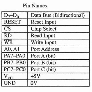
7 Pin Configuration of 8255 PA7-PA0: These are eight port A lines that acts as either latched output or buffered input lines depending upon the control word loaded into the control word register. PC7-PC4: Upper nibble of port C lines. They may act as either output latches or input buffers lines. This port also can be used for generation of handshake lines in mode 1 or mode 2. PC3-PC0: These are the lower port C lines, other details are the same as PC7-PC4 lines. PB0-PB7: These are the eight port B lines which are used as latched output lines or buffered input lines in the same way as port A. RD: This is the input line driven by the microprocessor and should be low to indicate read operation to 8255.
8 Pin Configuration of 8255 WR: This is an input line driven by the microprocessor. A low on this line indicates write operation. CS: This is a chip select line. If this line goes low, it enables the 8255 to respond to RD and WR signals, otherwise RD and WR signal are neglected. A1-A0: These are the address input lines and are driven by the microprocessor. These lines A1-A0 with RD, WR and CS from the following operations for These address lines are used for addressing any one of the four registers, i.e. three ports and a control word register as given in table below. In case of 8086 systems, if the 8255 is to be interfaced with lower order data bus, the A0 and A1 pins of 8255 are connected with A1 and A2 respectively.
9 Pin Configuration of 8255 D0-D7: These are the data bus lines those carry data or control word to/from the microprocessor. RESET: A logic high on this line clears the control word register of All ports are set as input ports by default after reset.
10 Operational Modes of 8255 There are two main operational modes of 8255: Input/output mode Bit set/reset mode
11 Operational Modes of 8255 Input / Output Mode There are three types of the input/output mode. Mode 0 In this mode, the ports can be used for simple input/output operations without handshaking. If both port A and B are initialized in mode 0, the two halves of port C can be either used together as an additional 8-bit port, or they can be used as individual 4-bit ports. Since the two halves of port C are independent, they may be used such that one-half is initialized as an input port while the other half is initialized as an output port. The input output features in mode 0 are as follows: O/p are latched. I/p are buffered not latched. Port do not have handshake or interrupt capability.
12 Mode 1 Operational Modes of 8255 When we wish to use port A or port B for handshake (strobed) input or output operation, we initialize that port in mode 1 (port A and port B can be initialized to operate in different modes, ie, for eg., port A can operate in mode 0 and port B in mode 1). Some of the pins of port C function as handshake lines. For port B in this mode (irrespective of whether is acting as an input port or output port), PC0, PC1 and PC2 pins function as handshake lines. If port A is initialized as mode 1 input port, then, PC3, PC4 and PC5 function as handshake signals. Pins PC6 and PC7 are available for use as input/output lines. The mode 1 which supports handshaking has following features: Two ports i.e. port A and B can be used as 8-bit I/O port. Each port uses three lines of port c as handshake signal and remaining two signals can be function as I/O port. Interrupt logic is supported. Input and Output data are latched.
13 Operational Modes of 8255 Mode 2 Only group A can be initialized in this mode. Port A can be used for bidirectional handshake data transfer. This means that data can be input or output on the same eight lines (PA0 - PA7). Pins PC3 - PC7 are used as handshake lines for port A. The remaining pins of port C (PC0 - PC2) can be used as input/output lines if group B is initialized in mode 0. In this mode, the 8255 may be used to extend the system bus to a slave microprocessor or to transfer data bytes to and from a floppy disk controller.
14 Operating Modes of the Bit Set/Reset (BSR) mode In this mode only port b can be used (as an output port). Each line of port C (PC0 - PC7) can be set/reset by suitably loading the command word register.no effect occurs in inputoutput mode. The individual bits of port c can be set or reset by sending the signal OUT instruction to the control register.

15 Control Word Format
16 Control Word Format This mode is selected by making D7 = '1'. D0, D1, D3, D4 are for lower port C, port B, upper port C and port A respectively. When D0 or D1 or D3 or D4 are "SET", the corresponding ports act as input ports. For eg, if D0 = D4 = '1', then lower port C and port A act as input ports. If these bits are "RESET", then the corresponding ports act as output ports. For eg, if D1 = D3 = '0', then port B and upper port C act as output ports. D2 is used for mode selection for group B (Port B and Lower Port C). When D2 = '0', mode 0 is selected and when D2 = '1', mode 1 is selected. D5, D6 are used for mode selection for group A (Upper Port C and Port A). The format is as follows:
 is SET, when D0 = '0', the port C bit is RESET.")
17 Control Word Format BSR mode format Control Word format in BSR mode The figure shows the control word format in BSR mode. This mode is selected by making D7='0'. D0 is used for bit set/reset. When D0= '1', the port C bit selected (selection of a port C bit is shown in the next point) is SET, when D0 = '0', the port C bit is RESET. D1, D2, D3 are used to select a particular port C bit whose value may be altered using D0 bit as mentioned above.
18 Control Word Format
19 THANK YOU
PIO 8255 (cont..) M Krishna kumar MAM/M3/LU9e/V1/2004 1
 M Krishna kumar MAM/M3/LU9e/V1/2004 1") PIO 8255 (cont..) The parallel input-output port chip 8255 is also called as programmable peripheral input-output port. The Intel s 8255 is designed for use with Intel s 8-bit, 16-bit and higher capability
PIO 8255 (cont..) The parallel input-output port chip 8255 is also called as programmable peripheral input-output port. The Intel s 8255 is designed for use with Intel s 8-bit, 16-bit and higher capability
CHAPTER: 3 PROGRAMMABLE PERIPHERAL INTERFACE & ELECTROMECHANICAL DEVICES INTERFACING
 CHAPTER: 3 1 PROGRAMMABLE PERIPHERAL INTERFACE & ELECTROMECHANICAL DEVICES INTERFACING Introduction to 8255 PPI 2 The Intel 8255A is a high-performance, general purpose programmable I/O device is designed
MAHALAKSHMI ENGINEERING COLLEGE TIRUCHIRAPALLI UNIT IV I/O INTERFACING PART A (2 Marks)
") MAHALAKSHMI ENGINEERING COLLEGE TIRUCHIRAPALLI-621213. UNIT IV I/O INTERFACING PART A (2 Marks) 1. Name the three modes used by the DMA processor to transfer data? [NOV/DEC 2006] Signal transfer mode (cycling
MAHALAKSHMI ENGINEERING COLLEGE TIRUCHIRAPALLI-621213. UNIT IV I/O INTERFACING PART A (2 Marks) 1. Name the three modes used by the DMA processor to transfer data? [NOV/DEC 2006] Signal transfer mode (cycling
Basic I/O Interface
 Basic I/O Interface - 8255 11 3 THE PROGRAMMABLE PERIPHERAL 82C55 programmable peripheral interface (PPI) is a popular, low-cost interface component found in many applications. The PPI has 24 pins for
I/O Design. Input / Output Instructions. Engineering 4862 Microprocessors. Lecture 23. Cheng Li
 Engineering 4862 Microprocessors Lecture 23 Cheng Li EN-4012 licheng@engr.mun.ca I/O Design When designing an I/O port, ensure that the port is only active when selected by the microprocessor Use latches
INTERFACING INTERFACING. Richa Upadhyay Prabhu. NMIMS s MPSTME February 25, 2016
 INTERFACING Richa Upadhyay Prabhu NMIMS s MPSTME richa.upadhyay@nmims.edu February 25, 2016 8255: Programmable Peripheral Interface or Programmable Input output Device Introduction METHODS OF DATA TRANSFER
 Page 1 of 18 Hardware Training Tools Data Acquisition I/O Cards Development Tools Pic Tutor 8255 CHIPS Software CAD Education Consulting Downloads PRICE LIST Corporate About AMS Chronology Contact Sales
Intel 8255 PPI. Presented By: Diwakar Yagyasen Asst. Prof. CSE BBDNITM, Lucknow.
 Intel 8255 PPI Presented By: Diwakar Yagyasen Asst. Prof. CSE BBDNITM, Lucknow. 8255 PPI PPI: Programmable Peripheral Interface 2 Intel 8255 PPI PPI Programmable Peripheral Interface It is an I/O port
Topics. Interfacing chips
 8086 Interfacing ICs 2 Topics Interfacing chips Programmable Communication Interface PCI (8251) Programmable Interval Timer (8253) Programmable Peripheral Interfacing - PPI (8255) Programmable DMA controller
Features: 3 8-bit IO ports PA, PB, PC. PA can be set for Modes 0, 1, 2. PB for 0,1 and PC for mode 0 and for BSR. Modes 1 and 2 are interrupt driven.
 Features: 3 8-bit IO ports PA, PB, PC PA can be set for Modes, 1, 2. PB for,1 and PC for mode and for BSR. Modes 1 and 2 are interrupt driven. PC has 2 4-bit parts: PC upper (PCU) and PC lower (PCL), each
Lecture-53 Mode 2: (Strobed Bidirectional bus I/O) This functional configuration provides means for communicating with a peripheral device on a
 This functional configuration provides means for communicating with a peripheral device on a") Lecture-53 Mode 2: (Strobed Bidirectional bus I/O) This functional configuration provides means for communicating with a peripheral device on a single 8-bit I/O data bus in both directions, i.e., for both
Lecture-53 Mode 2: (Strobed Bidirectional bus I/O) This functional configuration provides means for communicating with a peripheral device on a single 8-bit I/O data bus in both directions, i.e., for both
9. PERIPHERAL CHIPS 9a
 9. PERIPHERAL CHIPS 9a 8255: Programmable Peripheral Interface. Draw the pin diagram of PPI 8255. Ans. The pin diagram of 8255 is shown in Fig. 9a. PA 3 4 PA 4 PA2 2 39 PA 5 PA 3 38 PA 6 PA 4 37 PA7 RD
Summer 2003 Lecture 21 07/15/03
 Summer 2003 Lecture 21 07/15/03 Simple I/O Devices Simple i/o hardware generally refers to simple input or output ports. These devices generally accept external logic signals as input and allow the CPU
Lecture-50 Intel 8255A: Programming and Operating Modes
 Lecture-50 Intel 8255A: Programming and Operating Modes Operation Description: There are three basic modes of operation that can be selected by the system software. Mode 0: Basic Input/output Mode 1: Strobes
Segment A Programmable Peripheral Interface (PPI)
") Segment 6 8255A Programmable Peripheral Interface (PPI) Content Why 8255A? Handshaking and Handshaking Signal Parallel Data Transfer 8255A Internal Block Diagram Description of 8255A Internal Block Diagram
Segment 6 8255A Programmable Peripheral Interface (PPI) Content Why 8255A? Handshaking and Handshaking Signal Parallel Data Transfer 8255A Internal Block Diagram Description of 8255A Internal Block Diagram
UNIT III. 2. Non-maskable interrupts. 3. Software interrupt. 4. Internal interrupt
 UNIT III 8086 INTERRUPTS: An interrupt is the method of processing the microprocessor by peripheral device. An interrupt is used to cause a temporary halt in the execution of program. Microprocessor responds
Unit DMA CONTROLLER 8257
 DMA CONTROLLER 8257 In microprocessor based system, data transfer can be controlled by either software or hardware. To transfer data microprocessor has to do the following tasks: Fetch the instruction
Microprocessors and Microcontrollers (EE-231)
") Microprocessors and Microcontrollers (EE-231) Main Objectives 8088 and 80188 8-bit Memory Interface 8086 t0 80386SX 16-bit Memory Interface I/O Interfacing I/O Address Decoding More on Address Decoding
Microprocessors and Microcontrollers (EE-231) Main Objectives 8088 and 80188 8-bit Memory Interface 8086 t0 80386SX 16-bit Memory Interface I/O Interfacing I/O Address Decoding More on Address Decoding
General Purpose Programmable Peripheral Devices. Assistant Professor, EC Dept., Sankalchand Patel College of Engg.,Visnagar
 Chapter 15 General Purpose Programmable Peripheral Devices by Rahul Patel, Assistant Professor, EC Dept., Sankalchand Patel College of Engg.,Visnagar Microprocessor & Interfacing (140701) Rahul Patel 1
a8255 Features General Description Programmable Peripheral Interface Adapter
 a8255 Programmable Peripheral Interface Adapter September 1996, ver. 1 Features a8255 MegaCore function implementing a programmable peripheral interface adapter Optimized for FLEX and MAX architectures
82C55. Programmable Peripheral Interface. Interfacing Part III
 82C55 Programmable Peripheral Interface Interfacing Part III Review More on Address decoding Interface with memory Introduction to Programmable Peripheral Interface 82C55 About 82C55 The 82C55 is a popular
UNIT - II PERIPHERAL INTERFACING WITH 8085
 UNIT - II PERIPHERAL INTERFACING WITH 8085 Peripheral Interfacing is considered to be a main part of Microprocessor, as it is the only way to interact with the external world. The interfacing happens with
Week 7. Input/Output Interface Circuits and LSI Peripheral Devices
 Week 7 Input/Output Interface Circuits and LSI Peripheral Devices Core and Special Purpose I/O Interfaces Special purpose I/O interfaces display parallel printer interface serial communication interface
3. Controtlto specify the mode of transfer such as read or write 4. A control to start the DMA transfer
 DMA Controller The DMA controller needs the usual circuits of an interface to communicate the CPU and 10 device. In addition, it needs an address register, a word count register, and a set of address lines.
MICROPROCESSOR B.Tech. th ECE
 MICROPROCESSOR B.Tech. th ECE Submitted by: Er. Amita Sharma Dept. of ECE 11/24/2014 2 Microprocessor Architecture The microprocessor can be programmed to perform functions on given data by writing specific
MICROPROCESSORS & INTERFACING (A1423) C.Lokanath Reddy Assistant Professor.
 C.Lokanath Reddy Assistant Professor.") MICROPROCESSORS & INTERFACING (A1423) C.Lokanath Reddy Assistant Professor clreddy@vardhaman.org Department of Electronics and Communication Engineering VARDHAMAN COLLEGE OF ENGINEERING (AUTONOMOUS) Shamshabad,
MICROPROCESSORS & INTERFACING (A1423) C.Lokanath Reddy Assistant Professor clreddy@vardhaman.org Department of Electronics and Communication Engineering VARDHAMAN COLLEGE OF ENGINEERING (AUTONOMOUS) Shamshabad,
The 8255A: Programmable Peripheral Interface
 CMP:885 Peripherals Summary- EE39: Computer Organization, rchitecture and MicroProcessors http://www.ee.iitb.ac.in/ sumantra/courses/up/up.html The 855: Programmable Peripheral Interface PROGRMMER S VIEW
< W3150A+ / W5100 Application Note for SPI >
 < W3150A+ / W5100 Application Note for SPI > Introduction This application note describes how to set up the SPI in W3150A+ or W5100. Both the W3150A+ and W5100 have same architecture. W5100 is operated
Module 3. Embedded Systems I/O. Version 2 EE IIT, Kharagpur 1
 Module 3 Embedded Systems I/O Version 2 EE IIT, Kharagpur 1 Lesson 15 Interrupts Version 2 EE IIT, Kharagpur 2 Instructional Objectives After going through this lesson the student would learn Interrupts
EC2304-MICROPROCESSOR AND MICROCONROLLERS 2 marks questions and answers UNIT-I
 EC2304-MICROPROCESSOR AND MICROCONROLLERS 2 marks questions and answers 1. Define microprocessors? UNIT-I A semiconductor device(integrated circuit) manufactured by using the LSI technique. It includes
INTERFACING THE ISCC TO THE AND 8086
 APPLICATION NOTE INTERFACING THE ISCC TO THE 68 AND 886 INTRODUCTION The ISCC uses its flexible bus to interface with a variety of microprocessors and microcontrollers; included are the 68 and 886. The
Architecture of 8085 microprocessor
 Architecture of 8085 microprocessor 8085 consists of various units and each unit performs its own functions. The various units of a microprocessor are listed below Accumulator Arithmetic and logic Unit
PART B (5 x 16 =80) ADDRESS BUS The 8085 has eight signal lines, A15 A8 : Unidirectional, known as high order address.
 ADDRESS BUS The 8085 has eight signal lines, A15 A8 : Unidirectional, known as high order address.") PART B (5 x 16 =80) 1. Explain with a help of neat diagram of Pin out details of 8085 microprocessor. Intel 8085 consists of 40 pins and signal can be classified as follow: Address Bus. Data Bus. Control
PART B (5 x 16 =80) 1. Explain with a help of neat diagram of Pin out details of 8085 microprocessor. Intel 8085 consists of 40 pins and signal can be classified as follow: Address Bus. Data Bus. Control
CPE/EE 421 Microcomputers
 CPE/EE 421 Microcomputers THE 68000 CPU HARDWARE MODEL Instructor: Dr Aleksandar Milenkovic Lecture Notes Lecture 19 CPE/EE 421/521 Microcomputers 1 THE 68000 CPU HARDWARE MODEL Chapter 4 68000 interface
Ch 4. Standard Single Purpose Processors: Peripherals
 EE414 Embedded Systems Ch 4. Standard Single Purpose Processors: Peripherals Part 2/5: Parallel Interface Byung Kook Kim School of Electrical Engineering Korea Advanced Institute of Science and Technology
Syllabus: Microprocessors And Microcontrollers - 15CS44:
 Syllabus: Microprocessors And Microcontrollers - 15CS44: Module 3: 8255 I/O programming: I/O addresses MAP of x86 PC s, programming and interfacing the 8255. Text book: Muhammad Ali Mazidi, Janice GillispieMazidi,
TOPIC 6 LATCH. FIGURE 1 INTERFACING OF ROM/EPROM TO µc 8051.
 TOPIC 6 MEMORY AND I/O INTERFACING MEMORY INTERFACING i. External ROM (program memory) Interfacing P1 P0 D 0-D 7 P3 EA clock LATCH A 0 ROM/ A 7 EPROM A 8 Address lines A 15 PSEN OE FIGURE 1 INTERFACING
The Purpose of Interrupt
 Interrupts 3 Introduction In this chapter, the coverage of basic I/O and programmable peripheral interfaces is expanded by examining a technique called interrupt-processed I/O. An interrupt is a hardware-initiated
8086 Interrupts and Interrupt Responses:
 UNIT-III PART -A INTERRUPTS AND PROGRAMMABLE INTERRUPT CONTROLLERS Contents at a glance: 8086 Interrupts and Interrupt Responses Introduction to DOS and BIOS interrupts 8259A Priority Interrupt Controller
Interfacing Fundamentals
 CHAPTER Interfacing Fundamentals 3.1 Introduction There is no doubt that the microcomputer revolution will continue into the future and many will be required to specify and integrate microprocessors into
1. Define Peripherals. Explain I/O Bus and Interface Modules. Peripherals: Input-output device attached to the computer are also called peripherals.
 1. Define Peripherals. Explain I/O Bus and Interface Modules. Peripherals: Input-output device attached to the computer are also called peripherals. A typical communication link between the processor and
These three counters can be programmed for either binary or BCD count.
 S5 KTU 1 PROGRAMMABLE TIMER 8254/8253 The Intel 8253 and 8254 are Programmable Interval Timers (PTIs) designed for microprocessors to perform timing and counting functions using three 16-bit registers.
Pin Description, Status & Control Signals of 8085 Microprocessor
 Pin Description, Status & Control Signals of 8085 Microprocessor 1 Intel 8085 CPU Block Diagram 2 The 8085 Block Diagram Registers hold temporary data. Instruction register (IR) holds the currently executing
MP Assignment III. 1. An 8255A installed in a system has system base address E0D0H.
 MP Assignment III 1. An 8255A installed in a system has system base address E0D0H. i) Calculate the system addresses for the three ports and control register for this 8255A. System base address = E0D0H
INTRO TO I/O INTERFACE
 Basic I/O Interface Introduction This chapter outlines some of the basic methods of communications, both serial and parallel, between humans or machines and the microprocessor. We first introduce the basic
Address connections Data connections Selection connections
 Interface (cont..) We have four common types of memory: Read only memory ( ROM ) Flash memory ( EEPROM ) Static Random access memory ( SARAM ) Dynamic Random access memory ( DRAM ). Pin connections common
1. INTRODUCTION TO MICROPROCESSOR AND MICROCOMPUTER ARCHITECTURE:
 1. INTRODUCTION TO MICROPROCESSOR AND MICROCOMPUTER ARCHITECTURE: A microprocessor is a programmable electronics chip that has computing and decision making capabilities similar to central processing unit
Overview of Intel 80x86 µp
 CE444 ١ ٢ 8088/808 µp and Supporting Chips Overview of Intel 80x8 µp ٢ ١ 8088/808 µp ٣ Both are mostly the same with small differences. Both are of bit internal Data bus Both have 0 bit address bus Capable
CPE/EE 421/521 Fall 2004 Chapter 4 The CPU Hardware Model. Dr. Rhonda Kay Gaede UAH. The CPU Hardware Model - Overview
 CPE/EE 421/521 Fall 2004 Chapter 4 The 68000 CPU Hardware Model Dr. Rhonda Kay Gaede UAH Fall 2004 1 The 68000 CPU Hardware Model - Overview 68000 interface Timing diagram Minimal configuration using the
1. Internal Architecture of 8085 Microprocessor
 1. Internal Architecture of 8085 Microprocessor Control Unit Generates signals within up to carry out the instruction, which has been decoded. In reality causes certain connections between blocks of the
FIGURE Three EPROMs interfaced to the 8088 microprocessor.
 10 3 8088 AND 80188 (8-BIT) MEMORY INTERFACE: Basic 8088/80188 Memory Interface: The 8088 and 80188 microprocessors have an 8-bit data bus. The memory system must decode the address to select a memory
INPUT-OUTPUT ORGANIZATION
 INPUT-OUTPUT ORGANIZATION Peripheral Devices: The Input / output organization of computer depends upon the size of computer and the peripherals connected to it. The I/O Subsystem of the computer, provides
Embedded Systems Ch 5A. Parallel Interface (I)
") Embedded Systems Ch 5A. Parallel Interface (I) Byung Kook Kim Dept of EECS Korea Advanced Institute of Science and Technology Overview 1. Introduction to Parallel Ports 2. Input/Output Mechanisms 3. IEEE
Embedded Systems Ch 5A. Parallel Interface (I) Byung Kook Kim Dept of EECS Korea Advanced Institute of Science and Technology Overview 1. Introduction to Parallel Ports 2. Input/Output Mechanisms 3. IEEE
4 Multiplexer. Y Fig Keyboard Scan Matrix
 - 4 Multiplexer Microcontroller 3 Decoder X Y Fig. - Keyboard Scan Matrix 2 Prentice Hall, Inc. -2 Track Sector Head positioning Fig. -2 Hard Disk Format 2 Prentice Hall, Inc. -3 RGB electron guns R G
EE 390 Lab Manual, EE Department, KFUPM. Experiment #7. Introduction to Flight86 Microprocessor Trainer and Application Board
 Experiment #7 Introduction to Flight86 Microprocessor Trainer and Application Board 7.0 Objectives: The objective of this experiment is to introduce the Flight86 Microprocessor training kit and application
Lab2: 8255 Interfacing
 AL-Hussein Bin Talal University College of Engineering Department of Computer Engineering Computer Interfacing and Peripherals Lab Student Name: Student Number: Dr. Fadi Abu-Amara Eng. Huda Saqallah Lab2:
PAPER SOLUTION. Microprocessor & Microcontroller SESSIONAL 1
 PPER SOLUTION SESSIONL 1 Microprocessor & Microcontroller - 2017-18 Department of Electronics & Telecommunication Engineering ST. VINCENT PLLOTTI COLLEGE OF ENGINEERING & TECHNOLOGY Q.1 (a) Draw and explain
8051 I/O and Class 6 EE4380 Spring 03. Pari vallal Kannan. Center for Integrated Circuits and Systems University of Texas at Dallas
 8051 I/O and 8255 Class 6 EE4380 Spring 03 Pari vallal Kannan Center for Integrated Circuits and Systems University of Texas at Dallas Why I/O Ports Controllers need to get external inputs and produce
MCS6522 V E R S A T IL E IN T ERFACE A D A PTER
 PRELIMINARY DATA MOS TCCHNOLOOY, INC. VALLEY FORGE CORPORATE CENTER 1216) 666 7950 950 RITTENHOUSE ROAD. NORRISTOWN, PA 19401 SHEET NOVEMBER 1977 MCS6522 V E R S A T IL E IN T ERFACE A D A PTER DESCRIPTION
PIN DIAGRAM. Richa Upadhyay Prabhu. NMIMS s MPSTME January 19, 2016
 PIN DIAGRAM Richa Upadhyay Prabhu NMIMS s MPSTME richa.upadhyay@nmims.edu January 19, 2016 Richa Upadhyay Prabhu (MPSTME) 8080 Microprocessor January 19, 2016 1 / 51 Pin Diagram of 8086 Richa Upadhyay
MICROPROCESSOR MEMORY ORGANIZATION
 MICROPROCESSOR MEMORY ORGANIZATION 1 3.1 Introduction 3.2 Main memory 3.3 Microprocessor on-chip memory management unit and cache 2 A memory unit is an integral part of any microcomputer, and its primary
Lecture-51 INTEL 8259A Programmable Interrupt Controller
 Lecture-51 INTEL 8259A Programmable Interrupt Controller The 8259A is a programmable interrupt controller designed to work with Intel microprocessor 8080 A, 8085, 8086, 8088. The 8259 A interrupt controller
Northern India Engineering College, Delhi (GGSIP University) PAPER I
 PAPER I") PAPER I Q1.Explain IVT? ANS. interrupt vector table is a memory space for storing starting addresses of all the interrupt service routine. It stores CS:IP PAIR corresponding to each ISR. An interrupt vector
PAPER I Q1.Explain IVT? ANS. interrupt vector table is a memory space for storing starting addresses of all the interrupt service routine. It stores CS:IP PAIR corresponding to each ISR. An interrupt vector
MICROPROCESSOR AND MICROCONTROLLER BASED SYSTEMS
 MICROPROCESSOR AND MICROCONTROLLER BASED SYSTEMS UNIT I INTRODUCTION TO 8085 8085 Microprocessor - Architecture and its operation, Concept of instruction execution and timing diagrams, fundamentals of
Microprocessor Architecture
 Microprocessor - 8085 Architecture 8085 is pronounced as "eighty-eighty-five" microprocessor. It is an 8-bit microprocessor designed by Intel in 1977 using NMOS technology. It has the following configuration
LABORATORY 1 INTRODUCTION TO 8085 MICROPROCESSOR DEVELOPMENT SYSTEM BOARD
 LABORATORY 1 INTRODUCTION TO 8085 MICROPROCESSOR DEVELOPMENT SYSTEM BOARD 1. INTRODUCTION TO 8085 MICROPROCESSOR DEVELOPMENT SYSTEMS. The basic components of the 8085 Microprocessor Development System
The MC9S12 in Expanded Mode Using MSI logic to build ports Using MSI logic to build an output port Using MSI logic to build an input port
 The MC9S12 in Expanded Mode Using MSI logic to build ports Using MSI logic to build an output port Using MSI logic to build an input port A Simple Parallel Output Port We want a port which will write 8
Chapter NINE 8088,80286 MICROPROCESSORS AND ISA BUS
 Chapter NINE 8088,80286 MICROPROCESSORS AND ISA BUS OBJECTIVES this chapter enables the student to: State the function of the pins of the 8088. List the functions of the 8088 data, address, and control
Allmost all systems contain two main types of memory :
 Memory Interface Allmost all systems contain two main types of memory : read-only memory (ROM) system software and permanent system data random access memory (RAM) or read/write memory application software
Lecture Note On Microprocessor and Microcontroller Theory and Applications
 Lecture Note On Microprocessor and Microcontroller Theory and Applications MODULE: 1 1. INTRODUCTION TO MICROPROCESSOR AND MICROCOMPUTER ARCHITECTURE: A microprocessor is a programmable electronics chip
Unit-IV Peripheral Interfacing S.Sayeekumar, AP/RMDEEE
 Unit-IV Peripheral Interfacing S.Sayeekumar, AP/RMDEEE 8251 The 8251A is a programmable serial communication interface chip designed for synchronous and asynchronous serial data communication. It supports
8254 is a programmable interval timer. Which is widely used in clock driven digital circuits. with out timer there will not be proper synchronization
 8254 is a programmable interval timer. Which is widely used in clock driven digital circuits. with out timer there will not be proper synchronization between two devices. So it is very useful chip. The
ORCA Series 3 Microprocessor Interface
 Application Note ORCA Series 3 Microprocessor Interface ORCA Series 3 Microprocessor Interface Introduction With the increased demand of larger and faster FPGAs, one of the goals of FPGA designers is to
MICROPROCESSOR TECHNOLOGY
 MICROPROCESSOR TECHNOLOGY Assis. Prof. Hossam El-Din Moustafa Lecture 12 Ch.5 8086/8088 Hardware Specifications 22-Mar-15 1 The Buffered System If more than 10 unit loads are attached to any bus pin, the
3. The MC6802 MICROPROCESSOR
 3. The MC6802 MICROPROCESSOR This chapter provides hardware detail on the Motorola MC6802 microprocessor to enable the reader to use of this microprocessor. It is important to learn the operation and interfacing
INSTITUTE OF ENGINEERING AND MANAGEMENT, KOLKATA Microprocessor
 INSTITUTE OF ENGINEERING AND MANAGEMENT, KOLKATA Microprocessor Subject Name: Microprocessor and Microcontroller Year: 3 rd Year Subject Code: CS502 Semester: 5 th Module Day Assignment 1 Microprocessor
1-2 Chapter 1: The Beboputer Microcomputer
 1-2 Chapter 1: The Beboputer Microcomputer The Beboputer microcomputer In its broadest sense, a computer is a device that can accept information from the outside world, process that information using logical
Microprocessor Architecture. mywbut.com 1
 Microprocessor Architecture mywbut.com 1 Microprocessor Architecture The microprocessor can be programmed to perform functions on given data by writing specific instructions into its memory. The microprocessor
Introduction read-only memory random access memory
 Memory Interface Introduction Simple or complex, every microprocessorbased system has a memory system. Almost all systems contain two main types of memory: read-only memory (ROM) and random access memory
S.R.M. INSTITUTE OF SCIENCE & TECHNOLOGY SCHOOL OF ELECTRONICS & COMMUNICATION ENGINEERING
 S.R.M. INSTITUTE OF SCIENCE & TECHNOLOGY SCHOOL OF ELECTRONICS & COMMUNICATION ENGINEERING QUESTION BANK Subject Code : EC307 Subject Name : Microprocessor and Interfacing Year & Sem : III Year, V Sem
Chapter ELEVEN 8255 I/O PROGRAMMING
 Chapter ELEVEN 8255 I/O PROGRAMMING OBJECTIVES this chapter enables the student to: Code Assembly language instructions to read and write data to and from I/O ports. Diagram the design of peripheral I/O
To Interface The 8085 Microprocessor
 To Interface The 8085 Microprocessor A microprocessor has to be interfaced with various peripherals to perform various functions. Let's discuss about the Interfacing techniques in detail. Introduction
Design with Microprocessors
 Design with Microprocessors Year III Computer Science 1-st Semester Lecture 11: I/O transfer with x86 I/O Transfer I/O Instructions We discussed IN, OUT, INS and OUTS as instructions for the transfer of
Exercise 1: Static Control of a Data Bus
 Exercise 1: Static Control of a Data Bus EXERCISE OBJECTIVE When you have completed this exercise, you will be able to demonstrate the function of the CS signal and R/W signal in controlling data transfer
MEMORY-MAPPED I /O. Universiti Teknikal Malaysia Melaka. Input/Output System Design
 Universiti Teknikal Malaysia Melaka Faculty of Electronics and Computer Engineering Department of Computer Engineering BENM 2123 MICROPROCESSOR TECHNOLOGY Instead of connecting to auxiliary memory, address
Programmable Peripheral Interface (PPI) 8255A. CEN433 King Saud University Dr. Mohammed Amer Arafah
 8255A. CEN433 King Saud University Dr. Mohammed Amer Arafah") Programmable Peripheral Interface (PPI) 8255A CEN433 King Saud University Dr. 1 Functional Diagram 2 Pin Description 3 8255A Basic Operation A 1 A 0 Port 0 0 Port A 0 1 Port B 1 0 Port C 1 1 Control Word
Programmable Peripheral Interface (PPI) 8255A CEN433 King Saud University Dr. 1 Functional Diagram 2 Pin Description 3 8255A Basic Operation A 1 A 0 Port 0 0 Port A 0 1 Port B 1 0 Port C 1 1 Control Word
SYLLABUS UNIT - I 8086/8088 ARCHITECTURE AND INSTRUCTION SET
 1 SYLLABUS UNIT - I 8086/8088 ARCHITECTURE AND INSTRUCTION SET Intel 8086/8088 Architecture Segmented Memory, Minimum and Maximum Modes of Operation, Timing Diagram, Addressing Modes, Instruction Set,
Chapter 4 : Microprocessor System
 Chapter-4 Microprocessor System A microcomputer consists of a set of components or modules of three basic types CPU memory and I/O units which communicate with each other. PIN Configuration of 8085 Fig
The MC9S12 address, data and control buses The MC9S12 single-chip mode memory map Simplified write/read cycle. Address, Data and Control Buses
 EE 308 Spring 2013 The MC9S12 address, data and control buses The MC9S12 single-chip mode memory map Simplified write/read cycle The real MC9S12 multiplexed external bus Byte order in microprocessors How
8086 Hardware Specification
 Content: Segment 5 8086 Hardware Specification 8086 Modes of operation. Pin diagram and pin function of 8086. 8284A Clock generator operation and pin functions. Prepared By: Mohammed Abdul Kader Lecturer,
Lecture-55 System Interface:
 Lecture-55 System Interface: To interface 8253 with 8085A processor, CS signal is to be generated. Whenever CS =0, chip is selected and depending upon A 1 and A 0 one of the internal registers is selected
MICROPROCESSOR TECHNOLOGY
 MICROPROCESSOR TECHNOLOGY Assis. Prof. Hossam El-Din Moustafa Lecture 13 Ch.6 The 80186, 80188, and 80286 Microprocessors 21-Apr-15 1 Chapter Objectives Describe the hardware and software enhancements
Three-box Model: These three boxes need interconnecting (usually done by wiring known as a bus. 1. Processor CPU e.g. Pentium 4 2.
 Three-box Model: 1. Processor CPU e.g. Pentium 4 2. Storage - Memory 3. I/O input/output electronics for communication with other devices These three boxes need interconnecting (usually done by wiring
32- bit Microprocessor-Intel 80386
 32- bit Microprocessor-Intel 80386 30 Marks Course Outcome: Explain memory management and concept of pipelining. Describe the concept of paging and addressing. Signal Description of 80386 Signal Descriptions
2. List the five interrupt pins available in INTR, TRAP, RST 7.5, RST 6.5, RST 5.5.
 DHANALAKSHMI COLLEGE OF ENGINEERING DEPARTMENT OF ELECTRICAL AND ELECTRONICS ENGINEERING EE6502- MICROPROCESSORS AND MICROCONTROLLERS UNIT I: 8085 PROCESSOR PART A 1. What is the need for ALE signal in
Chapter TEN. Memory and Memory Interfacing
 Chapter TEN Memory and Memory Interfacing OBJECTIVES this chapter enables the student to: Define the terms capacity, organization, and speed as used in semiconductor memories. Calculate the chip capacity
PAS 9796/DIO ENGINEERING SPECIFICATION
 Document PAS018 DOC Revision C1 10/14/2009 PAS 9796/DIO ENGINEERING SPECIFICATION 160 CHANNEL VME DIGITAL INPUT / OUTPUT CARD Additional copies of this manual or other Precision Analog Systems (PAS) literature
ROEVER ENGINEERING COLLEGE
 ROEVER ENGINEERING COLLEGE ELAMBALUR, PERAMBALUR- 621 212 DEPARTMENT OF INFORMATION TECHNOLOGY MICROPROCESSOR & MICROCONTROLLER 2 marks questions andanswers Unit I 1. Define microprocessor? A microprocessor
Z8 Pod Adapter. for the. Fluke 9000-Series Troubleshooter
 Z8 Pod Adapter for the Fluke 9000-Series Troubleshooter May 23, 1984 Table of Contents 1. Conventions Used in This Document... 1 2. Overview... 2 3. Pod Adapter Setup... 3 3.1. Drivability Checking Control
Chapter 13 Direct Memory Access and DMA-Controlled I/O
 Chapter 13 Direct Memory Access and DMA-Controlled I/O The DMA I/O technique provides direct access to the memory while the microprocessor is temporarily disabled This allows data to be transferred between