Special Microarchitecture based on a lecture by Sanjay Rajopadhye modified by Yashwant Malaiya
|
|
|
- Della Jones
- 6 years ago
- Views:
Transcription

1 Special Microarchitecture based on a lecture by Sanjay Rajopadhye modified by Yashwant Malaiya


2 Computing Layers Problems Algorithms Language Instruction Set Architecture Microarchitecture Circuits Devices
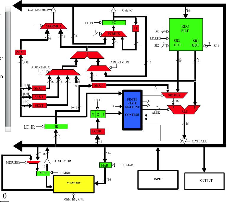
3 LC-3 Data Path Revisited Filled arrow = info to be processed. Unfilled arrow = control signal. 5-3
4 Microarchitecture Functional hardware blocks in a digital system With storage : Registers, Register file, Memory ØTriggerd by the system clock Combinational : MUXes, ALU, adder, SEXT, wiring etc. ØRespond after some propagation delay Design process: Design the datapath and identify control signals Design the Control Finite State Machine Design of functional blocks using gates and flip-flops will be studied later. 4
5 Timing relative to system clock Combinational blocks (Logic and wiring) Output is always a function of the values on input wires If input changes, the change propagates with some propagation delay. Storage elements are timed Clock a special signal that determines this timing Storage can be updated only at the tick of the clock What happens between ticks? The current values are processed by logic and wiring to produce values that will be used to update at the next tick How fast can the clock tick? Must allow for the longest combinational signal path 5
6 Timing relative to system clock How fast can the clock tick? Must allow for the longest combinational signal path. Clock frequency: tick rate Ex: 2 GHz mean 2x10 9 cycles per second Clock period: period between two pulses Inverse of clock frequency 2 GHz clock frequency means period is 0.5 nanosecond clock period. Signals must stabilize between two clock periods. Thus longest combinational signal path must be less than a clock period. 6
7 Register Transfer and Timing In one clock period, signals travel from a source register(s) to a destination register, through the combinational logic. Register transfer notation describes such transfer. For example: Condition: Rdest <- Rsource 1 + Rsource 2 Condition is the logical condition for which this transfer takes place (often in terms of control signals). Transfer takes one clock cycle. Memory operations assumed here to take one cycle also (in reality memories are slow, and take multiple cycles) Register transfer languages: Basic: here Advanced: VHDL, Verolog: used for description/design 7
8 Combinational Logic A digital circuit that computes a function of the inputs. Examples: Adder: takes X and Y and produces X + Y AND: takes X and Y, produces bitwise and NOT: takes X and Y and produces ~X 2-to-1 MUX: takes three inputs, X, Y and s (the last one is 1- bit) and produces (note that this is C-syntax, not the RTN that we will show later) (s==0)? X : Y 8
9 Wires and Busses Wires are (almost) just like electrical wires Directional (arrows), sometimes bidirectional May have a thickness: number of bits of data: e.g., the adder output is 16-bits in LC-3 Busses: Shared wires Anyone can read at all times Write is via arbitration (control signals to decide who gets to write on the bus) 9
10 Storage Elements Large scale storage (memory): view it like an array Address, Data in/out Small scale storage (registers): Programmer-visible registers: R0 R7 Special purpose registers: ØPC, IR, PSR (processor status register), MAR, MDR 10
11 Memory Processor issues commands to memory, who responds Mem.EN (memory enable): hey, I m talking to you Mem.RW: here s what I want you to do Two special registers Memory Address Register (MAR): only processor writes to this Memory Data Register (MDR): both processor/memory can write to this Ø the processor generates the control signals If Mem.EN and if Mem.RW==0, (i.e.., read) the memory outputs the value at address MAR, If Mem.RW==0, copy the contents of MDR into location Mem[MAR] 11
12 12 Registers Every register is connected to some inputs and has a special load signal. If load signal is 1 at the next clock tick the input is stored into the register Otherwise, no change in register contents (LD.PC & (PCMux = 10) )? PC ß PC+1 In terms of simple RTN notation Cycle 2: PC ß PC+1 Which assumes that during Cycle2 [LD.PC & (PCMux = 10)) is true.
13
14 Register Transfer Notation Compact, program-like notation Describe what happens in the datapath One or more transfers per clock tick one line = one clock tick Two columns: Write the desired transfers List control signals to effect the transfer Let s move on to LC3-Viz (special thanks, Joe Arnett) Corrections BR uses IR[8:0] instead of IR[10:0] for the PC offset 14
15 RTN/LC3-Viz Conventions Signals indicated must be asserted before the clock tick in order for the indicated transfer to occur. Sequence is: Signals are asserted Clock tick arrives, and causes the transfer In an RTN transfer, on either the right hand side (rhs), or left hand side (lhs) Mem[x] is the memory at address x Mem[MAR] is the memory at address that is in the MAR Reg[x] is Register number x 15
16 RTN Conventions An RTN transfer is of the form: LHS-location ß RHS-expression The LHSlocation may be a memory or a specific register or the x-th register The RHS-expression is: named registers, e.g., Reg[3] memory locations e.g., Mem[MAR] simple expressions PC+1, Reg[src] + Reg[dst] 16
17 17 How does the LC-3 fetch an instruction? # Transfer the PC into MAR Cycle 1: MAR ß PC # LD.MAR, GatePC # Read memory; increment PC Cycle 2: MDR ß Mem[MAR]; PC ß PC+1 # Transfer MDR into IR Cycle 3: IR ß MDR # LD.MDR, MDR.SEL, MEM.EN, LD.PC, PCMUX # LD.IR, GateMDR
18 Control Unit State Diagram The control unit is a state machine. Here is part of a simplified state diagram for the LC-3: A more complete state diagram is in Appendix C. It will be more understandable after Chapter
19 Control Unit State Diagram Appendix C. 4-19
20 20 How does the LC-3 decode the instruction? # Special decode step (controller makes decision, no clock cycle is wasted since it only involves logic) # No visible signal is active
21 21 How does the LC-3 execute a NOT instruction? # Src register contents are negated by ALU and result is stored in dst register Cycle 4: Reg[dst] ß ~Reg[src]; CC ß Sign(~Reg[src]) # LD.REG, DR = dst, GateALU, ALUK = ~, SR1 = src, LD.CC
22 Other instructions Every instruction is a sequence of transfers Every one has the same first three cycles (instruction fetch) Every one takes (at least one) additional cycle Some take even more more Each one effected by a specific set of control signals The Controller is responsible for generating the correct signals in the appropriate cycle Reminder Logic responds after some propagation dalay, Storage loads are on clock ticks 22
23 Data Path Components 5-23
24 Data Path Components Global bus special set of wires that carry a 16-bit signal to many components inputs to the bus are tri-state devices, that only place a signal on the bus when they are enabled only one (16-bit) signal should be enabled at any time Øcontrol unit decides which signal drives the bus any number of components can read the bus Øregister only captures bus data if it is write-enabled by the control unit Memory Control and data registers for memory and I/O devices memory: MAR, MDR (also control signal for read/write) 5-24
25 Data Path Components ALU Accepts inputs from register file and from sign-extended bits from IR (immediate field). Output goes to bus. Øused by condition code logic, register file, memory Register File Two read addresses (SR1, SR2), one write address (DR) Input from bus Øresult of ALU operation or memory read Two 16-bit outputs Øused by ALU, PC, memory address Ødata for store instructions passes through ALU 5-25
26 Data Path Components More details later. Multiplexer (MUX): selects data from multiple sources PC and PCMUX Three inputs to PC, controlled by PCMUX 1. PC+1 FETCH stage 2. Address adder BR, JMP 3. bus TRAP (discussed later) MAR and MARMUX Two inputs to MAR, controlled by MARMUX 1. Address adder LD/ST, LDR/STR 2. Zero-extended IR[7:0] -- TRAP (discussed later) 5-26
27 Data Path Components Condition Code Logic Looks at value on bus and generates N, Z, P signals Registers set only when control unit enables them (LD.CC) Øonly certain instructions set the codes (ADD, AND, NOT, LD, LDI, LDR, LEA) Control Unit Finite State Machine On each machine cycle, changes control signals for next phase of instruction processing Øwho drives the bus? (GatePC, GateALU, ) Øwhich registers are write enabled? (LD.IR, LD.REG, ) Øwhich operation should ALU perform? (ALUK) Ø Logic includes decoder for opcode, etc. 5-27
Copyright The McGraw-Hill Companies, Inc. Permission required for reproduction or display. Computing Layers
 Chapter 5 The LC-3 Original slides from Gregory Byrd, North Carolina State University Modified slides by C. Wilcox, S. Rajopadhye Colorado State University Computing Layers Problems Algorithms Language
LC-3 Instruction Processing
 LC-3 Instruction Processing (Textbookʼs Chapter 4)# Next set of Slides:# Textbook Chapter 10-10.2# Instruction Processing# It is impossible to do all of an instruction in one clock cycle.# Processors break
LC-3 Instruction Processing. (Textbook s Chapter 4)
") LC-3 Instruction Processing (Textbook s Chapter 4) Instruction Processing Fetch instruction from memory Decode instruction Evaluate address Fetch operands from memory Usually combine Execute operation
LC-3 Instruction Processing (Textbook s Chapter 4) Instruction Processing Fetch instruction from memory Decode instruction Evaluate address Fetch operands from memory Usually combine Execute operation
CS 2461: Computer Architecture I
 Computer Architecture is... CS 2461: Computer Architecture I Instructor: Prof. Bhagi Narahari Dept. of Computer Science Course URL: www.seas.gwu.edu/~bhagiweb/cs2461/ Instruction Set Architecture Organization
LC3DataPath ECE2893. Lecture 9a. ECE2893 LC3DataPath Spring / 14
 LC3DataPath ECE2893 Lecture 9a ECE2893 LC3DataPath Spring 2011 1 / 14 LC3 Data Path [4:0] FINITE MACHINE STATE MEMORY IR ADDR2MUX ADDR1MUX + GateMARMUX LDPC MARMUX ZEXT SEXT SEXT SEXT RESET GateALU +1
11/28/2016. ECE 120: Introduction to Computing. Register Loads Control Updates to Register Values. We Consider Five Groups of LC-3 Control Signals
 University of Illinois at Urbana-Champaign Dept. of Electrical and Computer Engineering ECE 120: Introduction to Computing LC-3 Control Signals Time to Examine a Processor s Control Signals in Detail Recall
EEL 5722C Field-Programmable Gate Array Design
 EEL 5722C Field-Programmable Gate Array Design Lecture 12: Pipelined Processor Design and Implementation Prof. Mingjie Lin Patt and Patel: Intro. to Computing System * Stanford EE271 notes 1 Instruction
Computing Layers. Chapter 5 The LC-3
 Computing Layers Problems Chapter 5 The LC-3 Original slides from Gregory Byrd, North Carolina State University Modified slides by Chris Wilcox, Colorado State University Algorithms Language Instruction
Chapter 5 The LC-3. ACKNOWLEDGEMENT: This lecture uses slides prepared by Gregory T. Byrd, North Carolina State University 5-2
 Chapter 5 The LC-3 ACKNOWLEDGEMENT: This lecture uses slides prepared by Gregory T. Byrd, North Carolina State University 5-2 Instruction Set Architecture ISA = All of the programmer-visible components
Introduction to Computer Engineering. CS/ECE 252, Fall 2016 Prof. Guri Sohi Computer Sciences Department University of Wisconsin Madison
 Introduction to Computer Engineering CS/ECE 252, Fall 2016 Prof. Guri Sohi Computer Sciences Department University of Wisconsin Madison Chapter 5 The LC-3 Instruction Set Architecture ISA = All of the
Introduction to Computer Engineering. Chapter 5 The LC-3. Instruction Set Architecture
 Introduction to Computer Engineering CS/ECE 252, Spring 200 Prof. David A. Wood Computer Sciences Department University of Wisconsin Madison Chapter 5 The LC-3 Adapted from Prof. Mark Hill s slides Instruction
Instruction Set Architecture
 Chapter 5 The LC-3 Instruction Set Architecture ISA = All of the programmer-visible components and operations of the computer memory organization address space -- how may locations can be addressed? addressibility
COSC121: Computer Systems: Review
 COSC121: Computer Systems: Review Jeremy Bolton, PhD Assistant Teaching Professor Constructed using materials: - Patt and Patel Introduction to Computing Systems (2nd) - Patterson and Hennessy Computer
COSC121: Computer Systems: Review
 COSC121: Computer Systems: Review Jeremy Bolton, PhD Assistant Teaching Professor Constructed using materials: - Patt and Patel Introduction to Computing Systems (2nd) - Patterson and Hennessy Computer
The LC-3 Instruction Set Architecture. ISA Overview Operate instructions Data Movement instructions Control Instructions LC-3 data path
 Chapter 5 The LC-3 Instruction Set Architecture ISA Overview Operate instructions Data Movement instructions Control Instructions LC-3 data path A specific ISA: The LC-3 We have: Reviewed data encoding
Introduction to Computer Engineering. CS/ECE 252, Spring 2017 Rahul Nayar Computer Sciences Department University of Wisconsin Madison
 Introduction to Computer Engineering CS/ECE 252, Spring 2017 Rahul Nayar Computer Sciences Department University of Wisconsin Madison Chapter 5 The LC-3 Announcements Homework 3 due today No class on Monday
Chapter 8 Input/Output
 Lecture on Introduction to Computing Systems Chapter 8 Input/Output An Hong han@ustc.edu.cn 0 Fall School of Computer Science and Technology 0/11/3 1 Review So far, we ve learned how to: compute with values
Computer Architecture. Lecture 5: Multi-Cycle and Microprogrammed Microarchitectures
 Computer Architecture Lecture 5: Multi-Cycle and Microprogrammed Microarchitectures Dr. Ahmed Sallam Based on original slides by Prof. Onur Mutlu Agenda for Today & Next Few Lectures Single-cycle Microarchitectures
Computer Architecture Lecture 6: Multi-Cycle and Microprogrammed Microarchitectures
 18-447 Computer Architecture Lecture 6: Multi-Cycle and Microprogrammed Microarchitectures Prof. Onur Mutlu Carnegie Mellon University Spring 2015, 1/28/2015 Agenda for Today & Next Few Lectures Single-cycle
( input = α output = λ move = L )
") basicarchitectures What we are looking for -- A general design/organization -- Some concept of generality and completeness -- A completely abstract view of machines a definition a completely (?) general
basicarchitectures What we are looking for -- A general design/organization -- Some concept of generality and completeness -- A completely abstract view of machines a definition a completely (?) general
LC-3 ISA - II. Lecture Topics. Lecture materials. Homework. Machine problem. Announcements. ECE 190 Lecture 10 February 17, 2011
 LC- ISA - II Lecture Topics LC- data movement instructions LC- control instructions LC- data path review Lecture materials Textbook 5. - 5.6 Textbook Appendix A. Homework HW due Wednesday February 2 at
CS 270 Fall 2013 Mock Final
 CS 270 Fall 2013 Mock Final Name(s) of student(s) Please read these instructions completely before proceeding, and sign below. Your exam will not be graded without your signature. This is the mock nal
The von Neumann Model
 chapter 4 The von Neumann Model We are now ready to raise our level of abstraction another notch. We will build on the logic structures that we studied in Chapter 3, both decision elements and storage
Microprogrammed Control. ECE 238L μseq 2006 Page 1
 Microprogrammed Control ECE 238L μseq 26 Page 1 Sample Control Unit FSM Add Ld Ld1 Ld2 Jsr Jsr1 F F1 F2 D Ldi Ldi1 Ldi2 Ldi3 Ldi4 Ldr Ldr1 Ldr2 Not Sti Sti1 Sti2 Sti3 Sti4 ECE 238L μseq 26 Page 2 Sample
10/31/2016. The LC-3 ISA Has Three Kinds of Opcodes. ECE 120: Introduction to Computing. ADD and AND Have Two Addressing Modes
 University of Illinois at Urbana-Champaign Dept. of Electrical and Computer Engineering ECE 120: Introduction to Computing The LC-3 Instruction Set Architecture The LC-3 ISA Has Three Kinds of Opcodes
Intro. to Computer Architecture Homework 4 CSE 240 Autumn 2005 DUE: Mon. 10 October 2005
 Name: 1 Intro. to Computer Architecture Homework 4 CSE 24 Autumn 25 DUE: Mon. 1 October 25 Write your answers on these pages. Additional pages may be attached (with staple) if necessary. Please ensure
Chapter 5 - ISA. 1.The Von Neumann Model. The Stored Program Computer. Von Neumann Model. Memory
 Chapter 5 - ISA 1.The Von Neumann Model The Stored Program Computer 1943: ENIAC Presper Eckert and John Mauchly -- first general electronic computer. (or was it John V. Atanasoff in 1939?) Hard-wired program
20/08/14. Computer Systems 1. Instruction Processing: FETCH. Instruction Processing: DECODE
 Computer Science 210 Computer Systems 1 Lecture 11 The Instruction Cycle Ch. 5: The LC-3 ISA Credits: McGraw-Hill slides prepared by Gregory T. Byrd, North Carolina State University Instruction Processing:
Copyright The McGraw-Hill Companies, Inc. Permission required for reproduction or display. Computing Layers
 Chapter 4 The Von Neumann Model Original slides from Gregory Byrd, North Carolina State University Modified slides by C. Wilcox, S. Rajopadhye, Colorado State University Computing Layers Problems Algorithms
Department of Electrical and Computer Engineering The University of Texas at Austin
 Department of Electrical and Computer Engineering The University of Texas at Austin EE 360N, Fall 2005 Yale Patt, Instructor Aater Suleman, Linda Bigelow, Jose Joao, Veynu Narasiman, TAs Final Exam, December,
CS 31: Intro to Systems Digital Logic. Kevin Webb Swarthmore College February 2, 2016
 CS 31: Intro to Systems Digital Logic Kevin Webb Swarthmore College February 2, 2016 Reading Quiz Today Hardware basics Machine memory models Digital signals Logic gates Circuits: Borrow some paper if
Register Files. Single Bus Architecture. Register Files. Single Bus Processor. Term Project: using VHDL. Accumulator based architecture
 Register Files DR 3 SelS Design and simulate the LC-3 processor using VHDL Term Project: Single Processor Decoder... R R3 R6...... mux mux S S SelDR 3 DRin Clock 3 SelS LC-3 Architecture 3 Register File
Chapter 4 The Von Neumann Model
 Chapter 4 The Von Neumann Model The Stored Program Computer 1943: ENIAC Presper Eckert and John Mauchly -- first general electronic computer. (or was it John V. Atananasoff in 1939?) Hard-wired program
CS 31: Intro to Systems Digital Logic. Kevin Webb Swarthmore College February 3, 2015
 CS 31: Intro to Systems Digital Logic Kevin Webb Swarthmore College February 3, 2015 Reading Quiz Today Hardware basics Machine memory models Digital signals Logic gates Circuits: Borrow some paper if
Department of Electrical and Computer Engineering The University of Texas at Austin
 Department of Electrical and Computer Engineering The University of Texas at Austin EE 360N, Fall 003 Yale Patt, Instructor Santhosh Srinath, Danny Lynch, TAs Exam 1, October 0, 003 Name: Problem 1 (0
REGISTER TRANSFER LANGUAGE
 REGISTER TRANSFER LANGUAGE The operations executed on the data stored in the registers are called micro operations. Classifications of micro operations Register transfer micro operations Arithmetic micro
Chapter 4 The Von Neumann Model
 Chapter 4 The Von Neumann Model The Stored Program Computer 1943: ENIAC Presper Eckert and John Mauchly -- first general electronic computer. (or was it John V. Atanasoff in 1939?) Hard-wired program --
Informatics 2C Computer Systems Practical 2 Deadline: 18th November 2009, 4:00 PM
 Informatics 2C Computer Systems Practical 2 Deadline: 18th November 2009, 4:00 PM 1 Introduction This practical is based on material in the Computer Systems thread of the course. Its aim is to increase
Levels in Processor Design
 Levels in Processor Design Circuit design Keywords: transistors, wires etc.results in gates, flip-flops etc. Logical design Putting gates (AND, NAND, ) and flip-flops together to build basic blocks such
Introduction to Computer Engineering. CS/ECE 252 Prof. Mark D. Hill Computer Sciences Department University of Wisconsin Madison
 Introduction to Computer Engineering CS/ECE 252 Prof. Mark D. Hill Computer Sciences Department University of Wisconsin Madison Chapter 4 The Von Neumann Model The Stored Program Computer 1943: ENIAC Presper
ECE260: Fundamentals of Computer Engineering
 Datapath for a Simplified Processor James Moscola Dept. of Engineering & Computer Science York College of Pennsylvania Based on Computer Organization and Design, 5th Edition by Patterson & Hennessy Introduction
Introduction to Computer. Chapter 5 The LC-3. Instruction Set Architecture
 Introduction to Computer Engineering ECE/CS 252, Fall 2010 Prof. Mikko Lipasti Department of Electrical and Computer Engineering University of Wisconsin Madison Chapter 5 The LC-3 Instruction Set Architecture
Parallel logic circuits
 Computer Mathematics Week 9 Parallel logic circuits College of Information cience and Engineering Ritsumeikan University last week the mathematics of logic circuits the foundation of all digital design
6.1 Combinational Circuits. George Boole ( ) Claude Shannon ( )
 Claude Shannon ( )") 6. Combinational Circuits George Boole (85 864) Claude Shannon (96 2) Signals and Wires Digital signals Binary (or logical ) values: or, on or off, high or low voltage Wires. Propagate digital signals
6. Combinational Circuits George Boole (85 864) Claude Shannon (96 2) Signals and Wires Digital signals Binary (or logical ) values: or, on or off, high or low voltage Wires. Propagate digital signals
LC-3. 3 bits for condition codes (more later) Fixed-length instructions, with 4-bit opcodes. IIT CS 350 S 18- Hale
 Fixed-length instructions, with 4-bit opcodes. IIT CS 350 S 18- Hale") LC-3 (Little computer version 3) 16-bit address width, 16-bit addressability. (Word size is 16 bits) 65K possible memory addresses Signed integers are 2 s complement 8 General purpose registers (GPRs),
LC-3 (Little computer version 3) 16-bit address width, 16-bit addressability. (Word size is 16 bits) 65K possible memory addresses Signed integers are 2 s complement 8 General purpose registers (GPRs),
Department of Electrical and Computer Engineering The University of Texas at Austin
 Department of Electrical and Computer Engineering The University of Texas at Austin EE 60N, Fall 00 Yale Patt, Instructor Santhosh Srinath, Danny Lynch, TAs Exam, November 9, 00 Name: Problem (0 points):
Department of Electrical and Computer Engineering The University of Texas at Austin
 Department of Electrical and Computer Engineering The University of Texas at Austin EE 360N, Spring 2003 Yale Patt, Instructor Hyesoon Kim, Onur Mutlu, Moinuddin Qureshi, Santhosh Srinath, TAs Exam 1,
Computer Science 324 Computer Architecture Mount Holyoke College Fall Topic Notes: Data Paths and Microprogramming
 Computer Science 324 Computer Architecture Mount Holyoke College Fall 2007 Topic Notes: Data Paths and Microprogramming We have spent time looking at the MIPS instruction set architecture and building
CS/ECE 252: INTRODUCTION TO COMPUTER ENGINEERING UNIVERSITY OF WISCONSIN MADISON. Instructor: Rahul Nayar TAs: Annie Lin, Mohit Verma
 CS/ECE 252: INTRODUCTION TO COMPUTER ENGINEERING UNIVERSITY OF WISCONSIN MADISON Instructor: Rahul Nayar TAs: Annie Lin, Mohit Verma Examination 2 In Class (50 minutes) Wednesday, March 8, 207 Weight:
LC-3 Instruction Set Architecture
 CMPE12 Notes LC-3 Instruction Set Architecture (Textbookʼs Chapter 5 and 6)# Instruction Set Architecture# ISA is all of the programmer-visible components and operations of the computer.# memory organization#
General purpose registers These are memory units within the CPU designed to hold temporary data.
 Von Neumann Architecture Single processor is used Each instruction in a program follows a linear sequence of fetch decode execute cycle Program and data are held in same main memory Stored program Concept
Chapter 4 The Von Neumann Model
 Chapter 4 The Von Neumann Model The Stored Program Computer 1943: ENIAC Presper Eckert and John Mauchly -- first general electronic computer. (or was it John V. Atanasoff in 1939?) Hard-wired program --
LC-3 Instruction Set Architecture. Textbook Chapter 5
 LC-3 Instruction Set Architecture Textbook Chapter 5 Instruction set architecture What is an instruction set architecture (ISA)? It is all of the programmer-visible components and operations of the computer
Processor (I) - datapath & control. Hwansoo Han
 - datapath & control. Hwansoo Han") Processor (I) - datapath & control Hwansoo Han Introduction CPU performance factors Instruction count - Determined by ISA and compiler CPI and Cycle time - Determined by CPU hardware We will examine two
Processor (I) - datapath & control Hwansoo Han Introduction CPU performance factors Instruction count - Determined by ISA and compiler CPI and Cycle time - Determined by CPU hardware We will examine two
Topic #6. Processor Design
 Topic #6 Processor Design Major Goals! To present the single-cycle implementation and to develop the student's understanding of combinational and clocked sequential circuits and the relationship between
Design of the MIPS Processor (contd)
") Design of the MIPS Processor (contd) First, revisit the datapath for add, sub, lw, sw. We will augment it to accommodate the beq and j instructions. Execution of branch instructions beq $at, $zero, L add
Design of the MIPS Processor (contd) First, revisit the datapath for add, sub, lw, sw. We will augment it to accommodate the beq and j instructions. Execution of branch instructions beq $at, $zero, L add
Chapter 5: The Processor: Datapath and Control
 Chapter 5: The Processor: Datapath and Control Overview Logic Design Conventions Building a Datapath and Control Unit Different Implementations of MIPS instruction set A simple implementation of a processor
RISC Design: Multi-Cycle Implementation
 RISC Design: Multi-Cycle Implementation Virendra Singh Associate Professor Computer Architecture and Dependable Systems Lab Department of Electrical Engineering Indian Institute of Technology Bombay http://www.ee.iitb.ac.in/~viren/
Binghamton University. CS-120 Summer LC3 Memory. Text: Introduction to Computer Systems : Sections 5.1.1, 5.3
 LC3 Memory Text: Introduction to Computer Systems : Sections 5.1.1, 5.3 John Von Neumann (1903-1957) Princeton / Institute for Advanced Studies Need to compute particle interactions during a nuclear reaction
Design of Digital Circuits Lecture 15: Pipelining. Prof. Onur Mutlu ETH Zurich Spring April 2017
 Design of Digital Circuits Lecture 5: Pipelining Prof. Onur Mutlu ETH Zurich Spring 27 3 April 27 Agenda for Today & Next Few Lectures! Single-cycle Microarchitectures! Multi-cycle and Microprogrammed
Design of the MIPS Processor
 Design of the MIPS Processor We will study the design of a simple version of MIPS that can support the following instructions: I-type instructions LW, SW R-type instructions, like ADD, SUB Conditional
Inf2C - Computer Systems Lecture Processor Design Single Cycle
 Inf2C - Computer Systems Lecture 10-11 Processor Design Single Cycle Boris Grot School of Informatics University of Edinburgh Previous lectures Combinational circuits Combinations of gates (INV, AND, OR,
Basic Processing Unit: Some Fundamental Concepts, Execution of a. Complete Instruction, Multiple Bus Organization, Hard-wired Control,
 UNIT - 7 Basic Processing Unit: Some Fundamental Concepts, Execution of a Complete Instruction, Multiple Bus Organization, Hard-wired Control, Microprogrammed Control Page 178 UNIT - 7 BASIC PROCESSING
Department of Electrical and Computer Engineering The University of Texas at Austin
 Department of Electrical and Computer Engineering The University of Texas at Austin EE 306, Fall 017 Yale Patt, Instructor Stephen Pruett, Siavash Zangeneh, Aniket Deshmukh, Zachary Susskind, Meiling Tang,
Implementing Another ISA, Basic Pipelining
 EE360N: Computer Architecture Lecture #4 Department of Electical and Computer Engineering The University of Texas at Austin September 24, 2008 Disclaimer: The contents of this document are scribe notes
ELEC 5200/6200 Computer Architecture and Design Spring 2017 Lecture 4: Datapath and Control
 ELEC 52/62 Computer Architecture and Design Spring 217 Lecture 4: Datapath and Control Ujjwal Guin, Assistant Professor Department of Electrical and Computer Engineering Auburn University, Auburn, AL 36849
The Big Picture: Where are We Now? EEM 486: Computer Architecture. Lecture 3. Designing a Single Cycle Datapath
 The Big Picture: Where are We Now? EEM 486: Computer Architecture Lecture 3 The Five Classic Components of a Computer Processor Input Control Memory Designing a Single Cycle path path Output Today s Topic:
Department of Electrical and Computer Engineering The University of Texas at Austin
 Department of Electrical and Computer Engineering The University of Texas at Austin EE N Spring 7 Y. N. Patt, Instructor Chirag Sakhuja, Sarbartha Banerjee, Jonathan Dahm, Arjun Teh, TAs Exam March, 7
CSE140: Components and Design Techniques for Digital Systems
 CSE4: Components and Design Techniques for Digital Systems Tajana Simunic Rosing Announcements and Outline Check webct grades, make sure everything is there and is correct Pick up graded d homework at
CPE 335. Basic MIPS Architecture Part II
 CPE 335 Computer Organization Basic MIPS Architecture Part II Dr. Iyad Jafar Adapted from Dr. Gheith Abandah slides http://www.abandah.com/gheith/courses/cpe335_s08/index.html CPE232 Basic MIPS Architecture
EE 3170 Microcontroller Applications
 EE 3170 Microcontroller Applications Lecture 4 : Processors, Computers, and Controllers - 1.2 (reading assignment), 1.3-1.5 Based on slides for ECE3170 by Profs. Kieckhafer, Davis, Tan, and Cischke Outline
The Processor. Z. Jerry Shi Department of Computer Science and Engineering University of Connecticut. CSE3666: Introduction to Computer Architecture
 The Processor Z. Jerry Shi Department of Computer Science and Engineering University of Connecticut CSE3666: Introduction to Computer Architecture Introduction CPU performance factors Instruction count
Chapter 4. The Processor
 Chapter 4 The Processor Introduction CPU performance factors Instruction count Determined by ISA and compiler CPI and Cycle time Determined by CPU hardware 4.1 Introduction We will examine two MIPS implementations
Logistics. IIT CS 350 S '17 - Hale
 Logistics Remember: Lab 5 due next week not this week. Finish it early though so you can move on to Lab 6! Lab 2 grades in BB Required reading posted (Patt & Patel Ch. 5) First exam during class next Wednesday
Department of Electrical and Computer Engineering The University of Texas at Austin
 Department of Electrical and Computer Engineering The University of Texas at Austin EE 0N, Fall 005 Yale Patt, Instructor Aater Suleman, Linda Bigelow, Jose Joao, Veynu Narasiman, TAs Exam, November, 005
CHAPTER 4: Register Transfer Language and Microoperations
 CS 224: Computer Organization S.KHABET CHAPTER 4: Register Transfer Language and Microoperations Outline Register Transfer Language Register Transfer Bus and Memory Transfers Arithmetic Microoperations
For Example: P: LOAD 5 R0. The command given here is used to load a data 5 to the register R0.
 Register Transfer Language Computers are the electronic devices which have several sets of digital hardware which are inter connected to exchange data. Digital hardware comprises of VLSI Chips which are
REGISTER TRANSFER AND MICROOPERATIONS
 REGISTER TRANSFER AND MICROOPERATIONS Register Transfer Language Register Transfer Bus and Memory Transfers Arithmetic Microoperations Logic Microoperations Shift Microoperations Arithmetic Logic Shift
REGISTER TRANSFER AND MICROOPERATIONS
 1 REGISTER TRANSFER AND MICROOPERATIONS Register Transfer Language Register Transfer Bus and Memory Transfers Arithmetic Microoperations Logic Microoperations Shift Microoperations Arithmetic Logic Shift
Department of Electrical and Computer Engineering The University of Texas at Austin
 Department of Electrical and Computer Engineering The University of Texas at Austin EE 306, Fall 2011 Yale Patt, Instructor Faruk Guvenilir, Milad Hashemi, Jennifer Davis, Garrett Galow, Ben Lin, Taylor
CPU Organization (Design)
") ISA Requirements CPU Organization (Design) Datapath Design: Capabilities & performance characteristics of principal Functional Units (FUs) needed by ISA instructions (e.g., Registers, ALU, Shifters, Logic
ISA Requirements CPU Organization (Design) Datapath Design: Capabilities & performance characteristics of principal Functional Units (FUs) needed by ISA instructions (e.g., Registers, ALU, Shifters, Logic
CO Computer Architecture and Programming Languages CAPL. Lecture 18 & 19
 CO2-3224 Computer Architecture and Programming Languages CAPL Lecture 8 & 9 Dr. Kinga Lipskoch Fall 27 Single Cycle Disadvantages & Advantages Uses the clock cycle inefficiently the clock cycle must be
Chapter 4. The Processor
 Chapter 4 The Processor Introduction CPU performance factors Instruction count Determined by ISA and compiler CPI and Cycle time Determined by CPU hardware We will examine two MIPS implementations A simplified
COMPUTER ARCHITECTURE AND ORGANIZATION Register Transfer and Micro-operations 1. Introduction A digital system is an interconnection of digital
 Register Transfer and Micro-operations 1. Introduction A digital system is an interconnection of digital hardware modules that accomplish a specific information-processing task. Digital systems vary in
RISC Processor Design
 RISC Processor Design Single Cycle Implementation - MIPS Virendra Singh Indian Institute of Science Bangalore virendra@computer.org Lecture 13 SE-273: Processor Design Feb 07, 2011 SE-273@SERC 1 Courtesy:
STRUCTURE OF DESKTOP COMPUTERS
 Page no: 1 UNIT 1 STRUCTURE OF DESKTOP COMPUTERS The desktop computers are the computers which are usually found on a home or office desk. They consist of processing unit, storage unit, visual display
Major and Minor States
 Major and Minor States We now consider the micro operations and control signals associated with the execution of each instruction in the ISA. The execution of each instruction is divided into three phases.
A 32-bit Processor: Sequencing and Output Logic
 Lecture 18 A 32-bit Processor: Sequencing and Output Logic Hardware Lecture 18 Slide 1 Last lecture we defined the data paths: Hardware Lecture 18 Slide 2 and we specified an instruction set: Instruction
Computer Architecture Programming the Basic Computer
 4. The Execution of the EXCHANGE Instruction The EXCHANGE routine reads the operand from the effective address and places it in DR. The contents of DR and AC are interchanged in the third microinstruction.
Computer Architecture
 Computer Architecture Lecture 1: Digital logic circuits The digital computer is a digital system that performs various computational tasks. Digital computers use the binary number system, which has two
CENG 3420 Computer Organization and Design. Lecture 06: MIPS Processor - I. Bei Yu
 CENG 342 Computer Organization and Design Lecture 6: MIPS Processor - I Bei Yu CEG342 L6. Spring 26 The Processor: Datapath & Control q We're ready to look at an implementation of the MIPS q Simplified
Department of Electrical and Computer Engineering The University of Texas at Austin
 Department of Electrical and Computer Engineering The University of Texas at Austin EE 46N Fall Y. N. Patt, Instructor Siavash Zangeneh, Ali Fakhrzadehgan, Steven Flolid, Matthew Normyle TAs Exam 1 October
CS311 Lecture: CPU Implementation: The Register Transfer Level, the Register Set, Data Paths, and the ALU
 CS311 Lecture: CPU Implementation: The Register Transfer Level, the Register Set, Data Paths, and the ALU Last revised October 15, 2007 Objectives: 1. To show how a CPU is constructed out of a regiser
Introduction to CPU Design
 ١ Introduction to CPU Design Computer Organization & Assembly Language Programming Dr Adnan Gutub aagutub at uqu.edu.sa [Adapted from slides of Dr. Kip Irvine: Assembly Language for Intel-Based Computers]
Mark Redekopp and Gandhi Puvvada, All rights reserved. EE 357 Unit 15. Single-Cycle CPU Datapath and Control
 EE 37 Unit Single-Cycle CPU path and Control CPU Organization Scope We will build a CPU to implement our subset of the MIPS ISA Memory Reference Instructions: Load Word (LW) Store Word (SW) Arithmetic
LECTURE 5. Single-Cycle Datapath and Control
 LECTURE 5 Single-Cycle Datapath and Control PROCESSORS In lecture 1, we reminded ourselves that the datapath and control are the two components that come together to be collectively known as the processor.
The Processor: Datapath & Control
 Chapter Five 1 The Processor: Datapath & Control We're ready to look at an implementation of the MIPS Simplified to contain only: memory-reference instructions: lw, sw arithmetic-logical instructions:
CSE 2021 COMPUTER ORGANIZATION
 CSE 2021 COMPUTER ORGANIZATION HUGH LAS CHESSER 1012U HUGH CHESSER CSEB 1012U W10-M Agenda Topics: 1. Multiple cycle implementation review 2. State Machine 3. Control Unit implementation for Multi-cycle
There are four registers involved in the fetch cycle: MAR, MBR, PC, and IR.
 CS 320 Ch. 20 The Control Unit Instructions are broken down into fetch, indirect, execute, and interrupt cycles. Each of these cycles, in turn, can be broken down into microoperations where a microoperation
ENEE 350 Computer Organization Fall, 2004 Project Part 2, due November 18, 2004
 ENEE 350 Computer Organization Fall, 2004 Project Part 2, due November 18, 2004 Objective In this second phase of the project, you will make a datapath for the instruction set you devised in part 1. This