Wafer Level Packaging & Bumping A view from a European Service Provider
|
|
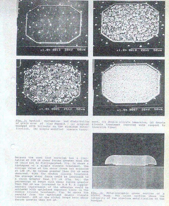
|
- Ronald Thomas
- 5 years ago
- Views:
Transcription
1 9 th International IEEE CPMT Symposium on High Density Design, Packaging and Microsystem Integration (HDP 07) 26 th -28 th June 2007 Shanghai, China Wafer Level Packaging & Bumping A view from a European Service Provider Thomas Oppert VP Marketing & Sales oppert@pactech.de
2 Content Overview on Semiconductor Markets 1970 to 2010 Applications and usage/implementation of eless NiAu ENIG UBM History & Now The early days of eless NiAu Licenses & worldwide wafer bumping capacity Pac Tech and eless NiAu now Equipment for eless NiAu Soldering Paste Printing Single Ball Placement Gang (Micro) Ball Placement Summary
3 Overview on Semiconductor Markets

4 Evolution Semiconductor Market Consumer/Wireless Internet Enterprise Military/ Aerospace Government Source: SIA
5 Semiconductor Market 2006 Cell Phone/ mobil 17,00% PC/ Computer 43,70% Wired Comm 7,00% Industrial/ Military 7,30% Consummer 17,20% Automotive 8,70%
6 Products using electroless Ni/Au First for products under very high price pressure (RFID) Meanwhile wide range of applications - ASIC (Sensors) - LCD Drivers - PowerMOS (Automotive) - Protection devices (Passives) CSP s, WLCSP s - Memories and memory modules - Consumer electronics - Mobile Phone - Medical (Ear phone)
7 Worldwide use of Pac Tech eless Ni & solder printing Medical; 10,00% LCD Driver/ ASIC; 5,00% Memory; 5,00% RFID; 20,00% Mobile Phone; 40,00% MOSFET; 20,00%
8 Electroless NiAu History & Now
9 Electroless Ni/Au for Semiconductor Devices A Crazy Idea? 1990 Technically impossible Wrong concept Not reliable No infrastructure Economically not feasible hard to control dangerous / critical Will be never accepted by customer Sounds familiar?

10 Remember: A Crazy Idea? 1886 Technically impossible Wrong concept Not reliable No infrastructure Economically not feasible hard to control dangerous / critical Will be never accepted by customer
11 History of electroless Pac Tech Basic studies & publications in 1985 First active electroless bumped wafer in 1989 Formation of Pac Tech in 1995 Further developments of the eless Ni UBM Pilot production line in 1997 Start of customer qualification & production in Pac Tech Wafer Bumping facilities in Germany, USA, Japan, Malaysia 10x Pac Tech eless NiAu Bumping process licensed and equipment installed worldwide


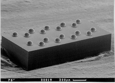
12 1st Ni Bumps 1990

13
14 more electroless Ni/Au ENIG NOT only for Al, also for Cu pads ENIG UBM for FC and Wire Bonding Eless Ni/Pd/Au for Wire Bond of Power Devices
15 Business Development Installed Equipment for ENIG UBM & Technology Transfer/Licenses of Pac Tech France Germany Telecom. 300 mm Malaysia Q3/ mm Taiwan Q4/ mm Japan Nagase 300 mm Telecom. Growth Japan (ABT) Subcon Korea (STW) LCD-Driver USA Memory 300 mm USA (PacTech) SubCon 300 mm Philippines Telecom. 300 mm USA Power Dev. France Q2/ Year
16 Pac Pac Tech Group Worldwide Wafer Bumping Capacity 2006 Pac Tech GmbH Pac Tech USA ABT ("Pac Tech Japan") <4-8" Wafer> 600k 600k 450k <12" Wafer> 100k 150k Pac Tech GmbH Pac Tech USA ABT ("Pac Tech Japan") Pac Tech Asia <4-8" Wafer> 600k 600k 600k 300k <12" Wafer> 100k 150k - 100k 2008 Pac Tech GmbH Pac Tech USA ABT ("Pac Tech Japan") Pac Tech Asia <4-8" Wafer> 600k 600k 600k 600k <12" Wafer> 100k 150k 150k 150k
17 Wafer Level UBM Electroless NiAu
18 Process Flow - Electroless Ni/Au Bumping Al Pad Cu Pad Zinkating Pd Seed Ni Plating Flash Au Pd Barrier Flash Au Flash Au Thick Au FCB Wire Bonding Wire Bonding
19 Under Bump Metal Process Electroless Plating of Ni/Au Bumps on Al pad 1/2 Backside Coating Pad Cleaning Pad Activation Electroless Nickel Flash Gold Coating Removal


20 Under Bump Metal Process Electroless Plating of Ni/Au Bumps on Al pad 2/2 Backside Coating Aluminum Cleaning Zincate Pretreatment Electroless Nickel Immersion Gold Coating Removal


21 Electroless Ni/Au on Copper Pad Backside Coating Pad Cleaning Pd Treatment Electroless Nickel 300 mm Capability! Flash Gold Coating Removal


22 Electroless Ni/Pd/Au Bumping on Al Backside Coating Aluminum Cleaning Zincate Pretreatment Electroless Nickel Electroless Palladium Immersion Gold Coating Removal


23 Flip Chip Modules for contactless Smart Cards Interconnection: Electroless NiAu with ACF


24 Pacline A mm 10 Plating Systems in the Field
 - Thick Au ability for wire bonding reliability - Ni bath control with ConPac 2.")

25 Pacline A50 - Capability for parallel processing of 3 carriers with 50 wafers 8 or 3 carriers with 26 wafers 12 - UPH: max. 150 Wafers 8"/hour or max. 78 wafers 12 /hour (5µm Ni/Au UBM) - Thick Au ability for wire bonding reliability - Ni bath control with ConPac 2.0 (bath conditioner) and ConPac control set - Central Computer Control Unit (CCCU) - PLC with Profi Bus system - Additional security tanks for each module and pump system - Design will be adapted to customer s facility - SECS GEM Interfacing - The system fulfils the fire safety standard FM 4910
26 Wafer Level Solder Printing
27 Comparison of Solder Bumping Technologies Evaporated Solder Bump Sputtered UBM + Plating Sputtered UBM + Print (FCT) Electroless UBM (+) (+) Print or Ball Attach C4 Solder Solder Solder Solder Au Ni/Au


28 Stencil Solder Printing Process Flow SnPb37, Lead-free: SnAgCu Electroless Ni/Au Bumping PbSn Solder Paste Printing Reflow Wafer Cleaning Wafer Inspection Pack & Ship


29 Applications for mobile phone GSM Phone: Battery Control Wafer: Si-Ge Technology Protection Devices


30 Solder Printing on 300mm Wafer I/O per Wafer 680 I/O per Chip 225µm pitch 100µm pad size 70µm solder ball height
31 Solder Ball Placement & Laser Reflow


32 Laser Soldering SB 2 -Jet


33 Semiautomatic SB²-SM SB 2 Equipment SB²-Jet LF with R2R Machines sold > 200 pcs SB²-Jet LF Automatic SB²-Jet 300 mm ESD version of SB²-Jet For HGA & HSA Assembly
34 SB 2 -Jet Advantages No tooling Solder ball diameters from 80(60)µm - 760µm Solder alloys: SnPb, SnAg, SnAgCu, AuSn No flux No mechanical stress/contact No thermal stress No additional reflow No cleaning of flux residues Fine pitch applications (110µm/100µm)

 Camera")
35 SB 2 -Applications Wafer Bumping BGA/ CSP Bumping Wafer Level CSP Bumping Rework/ Repair Optoelectronic Packaging SAW, BAW MEMS & 3-D Packaging Hard Disk Drive (HGA, HSA) Camera Modules


36 3D Assembly Design Considerations A B C
 Source:")
37 Fluxless 3D-Ball Placement & Laser Reflow on Flex Suspension for HDD (HGA) Source: Seagate
 Read / write transducer Electrical connections to read / write slider Electrical connections to drive coil Suspension Dateiname.")
38 Fluxless 3D-Ball Placement & Laser Reflow on Flex Suspension for HDD (HGA) Silicon stator (non-moving, attached to suspension) Silicon rotor (moving, holds magnet and slider Magnet/ buttom keeper Narrow beam flexure (connects rotor to stator) Read / write transducer Electrical connections to read / write slider Electrical connections to drive coil Suspension Dateiname.ppt 369
39 Gang (Micro) Ball Placement

40 Automatic Gang Ball Placer for Micro Ball Placement 1/2 Cassette to Cassette robot handling f. wafer up to 12 Integrated rework capability 100% yield 2x optical inspection 1st after ball transfer 2nd after repair min ball size 100µm pre- fluxing by printing/spraying UPH 5min/Wafer (8 ) 300 mm Capability! 1st fully auto machine already installed in Japan


41 Gang Ball Placer for Micro Ball Placement 2/2 8 Wafer Pitch 200µm I/O S 100µm solder balls SnAgCu


42 Wafer Level CSP Application eutectic SnPb or lead-free pitches: 180µm 1mm wafer sizes: 4 8 solder ball diameter: µm
43 Solder Ball Transfer by GBP - Ball Pickup Vacuum Solder Ball Bond Tool Mask 1 Vibration
44 Solder Ball Transfer by GBP Ball Placement Solder Ball Bond Tool Mask 2 Flux Wafer UBM 3
45 Ball Drop vs. Ball Transfer Placement Force Gravity only Ball Drop Process Weak solder bump adhesion to UBM due to insufficient flux wetting of solder ball Ball Escape out of dispense unit possible Ball Transfer Process much better fluxing process due to application of additional placement force Ball Escape not possible
46 Summary Overview on Semiconductor Markets Electroless NiAu UBM History & Now Eless NiAu for Al and Cu Eless NiPdAu Soldering Processes Paste Printing Single Ball Placement Gang (Micro) Ball Placement
47 Questions?
Wafer Probe card solutions
 Wafer Probe card solutions Innovative Solutions to Test Chips in the Semiconductor Industry Our long term experience in the electronic industry and our strong developing and process teams are inspired
Your Microelectronic Package Assembly Solution for MEMS Sensors. SMART Microsystems Ltd.
 Your Microelectronic Package Assembly Solution for MEMS Sensors Why MEMS is Important Growing Industry Segments About SMART Microsystems What We Do How We Do It Working with SMART 2 Why MEMS is Important
Embedded UTCP interposers for miniature smart sensors
 Embedded UTCP interposers for miniature smart sensors T. Sterken 1,2, M. Op de Beeck 2, Tom Torfs 2, F. Vermeiren 1,2, C. Van Hoof 2, J. Vanfleteren 1,2 1 CMST (affiliated with Ugent and IMEC), Technologiepark
Advanced CSP & Turnkey Solutions. Fumio Ohyama Tera Probe, Inc.
 Advanced CSP & Turnkey Solutions Fumio Ohyama Tera Probe, Inc. Tera Probe - Corporate Overview 1. Company : Tera Probe, Inc. 2. Founded : August, 2005 3. Capital : Approx. USD118.2 million (as of March
Challenges of Integration of Complex FHE Systems. Nancy Stoffel GE Global Research
 Challenges of Integration of Complex FHE Systems Nancy Stoffel GE Global Research Products drive requirements to sub-systems, components and electronics GE PRODUCTS CTQs: SWaP, $$, operating environment,
SMAFTI Package Technology Features Wide-Band and Large-Capacity Memory
 SMAFTI Package Technology Features Wide-Band and Large-Capacity Memory KURITA Yoichiro, SOEJIMA Koji, KAWANO Masaya Abstract and NEC Corporation have jointly developed an ultra-compact system-in-package
Wafer Probe card solutions
 Wafer Probe card solutions Innovative Solutions to Test Chips in the Semiconductor Industry Our long term experience in the electronic industry and our strong developing and process teams are inspired
SFC05-4 ChipClamp ΤΜ Flip Chip TVS Diode Array PRELIMINARY Features
 Description The SFC05-4 is a quad flip chip TVS array. They are state-of-the-art devices that utilize solid-state siliconavalanche technology for superior clamping performance and DC electrical characteristics.
Wafer Level Packaging The Promise Evolves Dr. Thomas Di Stefano Centipede Systems, Inc. IWLPC 2008
 Wafer Level Packaging The Promise Evolves Dr. Thomas Di Stefano Centipede Systems, Inc. IWLPC 2008 / DEVICE 1.E+03 1.E+02 1.E+01 1.E+00 1.E-01 1.E-02 1.E-03 1.E-04 1.E-05 1.E-06 1.E-07 Productivity Gains
Material technology enhances the density and the productivity of the package
 Material technology enhances the density and the productivity of the package May 31, 2018 Toshihisa Nonaka, Ph D. Packaging Solution Center Advanced Performance Materials Business Headquarter Hitachi Chemical
IPC-D-859. Design Standard for Thick Film Multilayer Hybrid Circuits ANSI/IPC-D-859. The Institute for. Interconnecting
 The Institute for Interconnecting and Packaging Electronic Circuits Design Standard for Thick Film Multilayer Hybrid Circuits ANSI/ Original Publication December 1989 A standard developed by the Institute
Reflow Soldering of MEMS Microphones
 Reflow Soldering of MEMS Microphones Page 1 of 7 Introduction This application note provides guidance and suggestions for assembling boards with MEMS microphones. Parameter and profile details are presented,
Micro SMD Wafer Level Chip Scale Package
 Micro SMD Wafer Level Chip Scale Package CONTENTS Package Construction Key attributes for micro SMD 4, 5, and 8 bump Smallest Footprint Micro SMD Handling Surface Mount Technology (SMT) Assembly Considerations
Bringing 3D Integration to Packaging Mainstream
 Bringing 3D Integration to Packaging Mainstream Enabling a Microelectronic World MEPTEC Nov 2012 Choon Lee Technology HQ, Amkor Highlighted TSV in Packaging TSMC reveals plan for 3DIC design based on silicon
AT&S Company. Presentation. 3D Component Packaging. in Organic Substrate. Embedded Component. Mark Beesley IPC Apex 2012, San Diego.
 3D Component Packaging AT&S Company in Organic Substrate Presentation Embedded Component Mark Beesley IPC Apex 2012, San Diego www.ats.net Austria Technologie & Systemtechnik Aktiengesellschaft Fabriksgasse13
Packaging Challenges for High Performance Mixed Signal Products. Caroline Beelen-Hendrikx, Eef Bagerman Semi Networking Day Porto, June 27, 2013
 Packaging Challenges for High Performance Mixed Signal Products Caroline Beelen-Hendrikx, Eef Bagerman Semi Networking Day Porto, June 27, 2013 Content HPMS introduction Assembly technology drivers for
Comparison & highlight on the last 3D TSV technologies trends Romain Fraux
 Comparison & highlight on the last 3D TSV technologies trends Romain Fraux Advanced Packaging & MEMS Project Manager European 3D Summit 18 20 January, 2016 Outline About System Plus Consulting 2015 3D
Embedded Power Dies for System-in-Package (SiP)
") Embedded Power Dies for System-in-Package (SiP) D. Manessis, L. Boettcher, S. Karaszkiewicz, R.Patzelt, D. Schuetze, A. Podlasky, A. Ostmann Fraunhofer Institute for Reliability and Microintegration (IZM),
Embedded Power Dies for System-in-Package (SiP) D. Manessis, L. Boettcher, S. Karaszkiewicz, R.Patzelt, D. Schuetze, A. Podlasky, A. Ostmann Fraunhofer Institute for Reliability and Microintegration (IZM),
Module 7 Electronics Systems Packaging
 Module 7 Electronics Systems Packaging Component Assembly, materials for assembly and joining methods in electronics -Surface Mount technology- design, fabrication and assembly; -failures library; -materials
Comparison of Singulation Techniques
 Comparison of Singulation Techniques Electronic Packaging Society, Silicon Valley Chapter Sept. 28, 2017 ANNETTE TENG Sept 28, 2017 1 Definition of Singulation 9/28/2017 Annetteteng@promex-ind.com 2 www.cpmt.org/scv
Packaging Technology for Image-Processing LSI
 Packaging Technology for Image-Processing LSI Yoshiyuki Yoneda Kouichi Nakamura The main function of a semiconductor package is to reliably transmit electric signals from minute electrode pads formed on
3D technology for Advanced Medical Devices Applications
 3D technology for Advanced Medical Devices Applications By, Dr Pascal Couderc,Jerome Noiray, Dr Christian Val, Dr Nadia Boulay IMAPS MEDICAL WORKSHOP DECEMBER 4 & 5,2012 P.COUDERC 3D technology for Advanced
onlinecomponents.com
 0.9 For FPC FPC connectors (0.3mm pitch) Back lock Y3B Series New FEATURES 1. Slim and low profile design (Pitch: 0.3 mm) The use of a back lock mechanism enables a 3.15 mm (with lever) low profile design.
P4S. High reliability, space saving type, 1.5 to 3.0 mm mated height
 For board-to-board For board-to-fpc Narrow pitch connectors (0.4mm pitch) P4S High reliability, space saving type, 1.5 to 3.0 mm mated height FEATURES 1. TOUGH CONTACT construction provides high resistance
onlinecomponents.com
 YF53 For FPC/FFC* FPC connectors (0.5mm pitch) Back lock / Series New Low profile and space saving body of 1.0 mm high and mm deep (3.70 mm including the lever) and can have a minimum of four and two contacts
DEPARTMENT WAFER LEVEL SYSTEM INTEGRATION
 FRAUNHOFER INSTITUTE FOR RELIABILITY AND MICROINTEGRATION IZM DEPARTMENT WAFER LEVEL SYSTEM INTEGRATION ALL SILICON SYSTEM INTEGRATION DRESDEN ASSID ALL SILICON SYSTEM INTEGRATION DRESDEN FRAUNHOFER IZM-ASSID
Application Note 5363
 Surface Laminar Circuit (SLC) Ball Grid Array (BGA) Lead-free Surface Mount Assembly Application Note 5363 Introduction This document outlines the design and assembly guidelines for surface laminar circuitry
Solder Reflow Guide for Surface Mount Devices Technical Note
 Solder Reflow Guide for Surface Mount Devices FPGA-TN-02041 Version 3.8 November 2017 Contents Acronyms in This Document... 3 1. Introduction... 4 2. Reflow... 4 3. Inspection... 4 4. Cleaning Recommendations...
AN-100 MEMS Microphone Handling and Assembly Guide
 MEMS Microphone Handling and Assembly Guide PURPOSE AND SCOPE This document provides information and general guidelines for handling and assembling boards with InvenSense Micro Electro- Mechanical Systems
An integrated solution for KGD: At-speed wafer-level testing and full-contact wafer-level burn-in after flip chip bumping
 An integrated solution for KGD: At-speed wafer-level testing and full-contact wafer-level burn-in after flip chip bumping Yuan-Ping Tseng/ An-Hong Liu TD center ChipMOS Technologies Inc. June 5, 2001 1
Packaging of Selected Advanced Logic in 2x and 1x nodes. 1 I TechInsights
 Packaging of Selected Advanced Logic in 2x and 1x nodes 1 I TechInsights Logic: LOGIC: Packaging of Selected Advanced Devices in 2x and 1x nodes Xilinx-Kintex 7XC 7 XC7K325T TSMC 28 nm HPL HKMG planar
Advanced Packaging For Mobile and Growth Products
 Advanced Packaging For Mobile and Growth Products Steve Anderson, Senior Director Product and Technology Marketing, STATS ChipPAC Growing Needs for Silicon & Package Integration Packaging Trend Implication
APPLICATION SPECIFICATION
 1 of 21 F 1.0 OBJECTIVE The objective of this specification is to provide information to assist with the application and use of MEG- Array High Speed Mezzanine BGA (Ball Grid Array) connectors system.
Solder Reflow Guide for Surface Mount Devices
 April 2008 Introduction Technical Note TN1076 This technical note provides general guidelines for a solder reflow and rework process for Lattice surface mount products. The data used in this document is
Ceramic Column Grid Array
 Application Note AC190 Ceramic Column Grid Array Table of Contents Introduction................................................ 1 CCGA Package Description....................................... 2 Column
FPC connectors (0.2mm pitch) Back lock
 Back lock") 0.9 AYF21 For FPC FPC connectors (0.2mm pitch) Back lock Y2B Series New FEATURES 1. Slim and low profile design (Pitch: 0.2 mm) 0.2 mm pitch back lock design and the slim body with a 3.15 mm depth (with
0.9 AYF21 For FPC FPC connectors (0.2mm pitch) Back lock Y2B Series New FEATURES 1. Slim and low profile design (Pitch: 0.2 mm) 0.2 mm pitch back lock design and the slim body with a 3.15 mm depth (with
REFLOW SOLDERING AND BOARD ASSEMBLY
 MEMS Microphone Handling and Assembly Guide PURPOSE AND SCOPE This document provides information and general guidelines for handling and assembling boards with InvenSense Micro Electro- Mechanical Systems
LCD and Camera EMI Filter Array with ESD Protection
 LCD and Camera EMI Filter Array with ESD Protection Features Six and eight channels of EMI filtering with integrated ESD protection 0.4mm pitch, 15-bump, 2.360mm x 1.053mm footprint Chip Scale Package
3-D Package Integration Enabling Technologies
 3-D Package Integration Enabling Technologies Nanium - Semi Networking Day David Clark - Choon Heung Lee - Ron Huemoeller June 27th, 2013 Enabling a Microelectronic World Mobile Communications Driving
Test Development Validation Production. Micro-BGA Socketing Systems BGA Socket Adapter Systems Flip-Top BGA Sockets BGA Interposers
 Test Development Validation Production Micro-BGA Socketing Systems BGA Socket Adapter Systems Flip-Top BGA Sockets BGA Interposers BGA Socket Adapter Systems Micro-BGA Socket Adapter System 0.50mm and
DISTRIBUTION LIST CHANGE RECORD
 DISTRIBUTION LIST In charge of the document: Fabrice Soufflet Process Engineering Group Copy to: Pierre Maurice Marie-Cécile Vassal Dominique Blain Pierre Wang Responsibility President Project Group Manager
Burn-in & Test Socket Workshop
 Burn-in & Test Socket Workshop IEEE March 4-7, 2001 Hilton Mesa Pavilion Hotel Mesa, Arizona IEEE COMPUTER SOCIETY Sponsored By The IEEE Computer Society Test Technology Technical Council COPYRIGHT NOTICE
ADVANCED PACKAGE REWORK
 ADVANCED PACKAGE REWORK SCORPION PRODUCT TRAINING VER.02-2018 2018 DESCO INDUSTRIES For support issues: www.smarttec.dk Scorpion Product Range Scorpion APR-1100-SRS Single head with vision alignment accuracy
Pushing the barriers of wafer level device integration: High-speed assembly, the case for MicroTape.
 Pushing the barriers of wafer level device integration: High-speed assembly, the case for MicroTape. Gordon Christison Reel Service Ltd 55 Nasmyth Road Southfield Industrial Estate Glenrothes Scotland
For board-to-fpc. Narrow pitch connectors (0.35mm pitch)
") For board-to-fpc Narrow pitch connectors (0.35mm pitch) A35S Contributes to device miniaturization and advanced functionality with 2.5 mm width, 0.35 mm pitch and 0.8 mm mated height! FEATURES 1. 0.35
For board-to-fpc Narrow pitch connectors (0.35mm pitch) A35S Contributes to device miniaturization and advanced functionality with 2.5 mm width, 0.35 mm pitch and 0.8 mm mated height! FEATURES 1. 0.35
Product Configuration Solder Tail Press-fit Tail MBCE Vertical Receptacle Yes Yes MBCE Right Angle Receptacle Yes / MBCE Straddle Mount Yes /
 Application Specification 114-128016 28 FEB 17 Rev A3 NOTE All numerical values are in metric units [with U.S. customary units in brackets]. Dimensions are in millimeters [and inches]. Unless otherwise
Test Development Validation Production. Micro-BGA Socketing System BGA Socket Adapter System Flip-Top BGA Socket BGA Interposer
 Test Development Validation Production Micro-BGA Socketing System BGA Socket Adapter System Flip-Top BGA Socket BGA Interposer BGA Socket Adapter Systems Micro-BGA Socket Adapter System 0.50mm and 0.65mm
From 3D Toolbox to 3D Integration: Examples of Successful 3D Applicative Demonstrators N.Sillon. CEA. All rights reserved
 From 3D Toolbox to 3D Integration: Examples of Successful 3D Applicative Demonstrators N.Sillon Agenda Introduction 2,5D: Silicon Interposer 3DIC: Wide I/O Memory-On-Logic 3D Packaging: X-Ray sensor Conclusion
Narrow pitch connectors (0.4mm pitch) Radiation noise reduced by multi-point ground and shield construction
 Radiation noise reduced by multi-point ground and shield construction") For board-to-board For board-to-fpc Narrow pitch connectors (0.4mm pitch) P4S Shield type Radiation noise reduced by multi-point ground and shield construction FEATURES 1. Radiation noise is reduced thanks
For board-to-board For board-to-fpc Narrow pitch connectors (0.4mm pitch) P4S Shield type Radiation noise reduced by multi-point ground and shield construction FEATURES 1. Radiation noise is reduced thanks
Study of Various PCBA Surface Finishes
 Study of Various PCBA Surface Finishes Georgie Thein, David Geiger, and Murad Kurwa Flextronics International Milpitas, California Abstract In this study various printed circuit board surface finishes
Technology Platform and Trend for SiP Substrate. Steve Chiang, Ph.D CSO of Unimicron Technology
 Technology Platform and Trend for SiP Substrate Steve Chiang, Ph.D CSO of Unimicron Technology Contents Unimicron Introduction SiP Evolution Unimicron SiP platform - PCB, RF, Substrate, Glass RDL Connector.
For board-to-fpc. Narrow pitch connectors (0.4mm pitch)
") For board-to-fpc Narrow pitch connectors (0.4mm pitch) A4S Being 2.5 mm in width, it facilitates ever-increasing device miniaturization and advanced functionality! FEATURES 1. TOUGH CONTACT construction
For board-to-fpc Narrow pitch connectors (0.4mm pitch) A4S Being 2.5 mm in width, it facilitates ever-increasing device miniaturization and advanced functionality! FEATURES 1. TOUGH CONTACT construction
Dispensing Applications and Methods. August, 2014 Mani Ahmadi, Director of Technical Services Nordson, Advanced Technology Systems
 Dispensing Applications and Methods August, 2014 Mani Ahmadi, Director of Technical Services Nordson, Advanced Technology Systems 1 August 2014 Agenda Introduction Dispensing method and technologies for
Packaging for parallel optical interconnects with on-chip optical access
 Packaging for parallel optical interconnects with on-chip optical access I. INTRODUCTION Parallel optical interconnects requires the integration of lasers and detectors directly on the CMOS chip. In the
ONYX 32 MULTIFUNCTIONAL POSITIONING AND SOLDERING SYSTEM
 ONYX MULTIFUNCTIONAL POSITIONING AND SOLDERING SYSTEM MACHINES.0 APPLICATION: SMT ZEVAC-LINE: ONYX The complete ONYX product line documentation is composed of the following data sheets: MACHINES.0 ACCESSORIES.0,.0
Advancing high performance heterogeneous integration through die stacking
 Advancing high performance heterogeneous integration through die stacking Suresh Ramalingam Senior Director, Advanced Packaging European 3D TSV Summit Jan 22 23, 2013 The First Wave of 3D ICs Perfecting
MPS2R Datasheet 100 MHz 6 GHz 40 W RoHS-Compliant Monolithic SPDT PIN Switch
 MPS2R11-608 Datasheet 100 MHz 6 GHz 40 W RoHS-Compliant Monolithic SPDT PIN Switch Microsemi makes no warranty, representation, or guarantee regarding the information contained herein or the suitability
Applications, Processing and Integration Options for High Dielectric Constant Multi-Layer Thin-Film Barium Strontium Titanate (BST) Capacitors
 Capacitors") Applications, Processing and Integration Options for High Dielectric Constant Multi-Layer Thin-Film Barium Strontium Titanate (BST) Capacitors Agenda Introduction What is BST? Unique Characteristics of
Applications, Processing and Integration Options for High Dielectric Constant Multi-Layer Thin-Film Barium Strontium Titanate (BST) Capacitors Agenda Introduction What is BST? Unique Characteristics of
Physical Design Implementation for 3D IC Methodology and Tools. Dave Noice Vassilios Gerousis
 I NVENTIVE Physical Design Implementation for 3D IC Methodology and Tools Dave Noice Vassilios Gerousis Outline 3D IC Physical components Modeling 3D IC Stack Configuration Physical Design With TSV Summary
Advanced BGA Rework Station. Suitable for all kind of reworks on different SMT components
 Advanced BGA Rework Station Suitable for all kind of reworks on different SMT components Advanced BGA Rework Station New Key Features Compact and Stable Design Larger Board Holding Capacity One Touch Lock
Ceramic Column Grid Array
 Application Note AC190 Ceramic Column Grid Array Introduction Ceramic Column Grid Array (CCGA) packages are becoming increasingly popular as an alternative to Ceramic Ball Grid Array (CBGA) packages for
Assembly Considerations for Linear Technology Module TM BGA Packages. July
 Assembly Considerations for Linear Technology Module TM BGA Packages July 2012 Package Construction PCB Design Guidelines Outline Moisture Sensitivity, Pack, Ship & Bake Board Assembly Process Screen Print
Setting the Test Standard for Tomorrow. Nasdaq: AEHR
 Setting the Test Standard for Tomorrow Nasdaq: AEHR Forward Looking Statements This presentation contains forward-looking statements that involve risks and uncertainties relating to projections regarding
Design and Assembly Process Implementation for BGAs
 ASSOCIATION CONNECTING ELECTRONICS INDUSTRIES Design and Assembly Process Implementation for BGAs Developed by the Device Manufacturers Interface Committee of IPC October 25, 2000 Users of this standard
Pb-free Update For the PSMC
 Pb-free Update For the PSMC 31 October 2017 Chair, PERM Steering Committee +1 978-858-9820 (tel) This document does not contain technology or technical data controlled under either the U.S. International
Printed Circuit Boards European Production
 Services of our European production We provide PCBs of up to 48 layers from selected European suppliers. Here we do not only focus on the price but on a reasonable value for money. Based on a detailed
at surface mount speeds
 www.uic.com email: universal@uic.com AMERICAS Tel. 1-800-432-2607 or Tel. +1-607-779-7522 CHINA, SHENZHEN Tel. +86-755-2685-9108 CHINA, SHANGHAI Tel. +86-21-6495-2100 EUROPE Tel. +421-2-4930-96-60 2017
Circuit Board Guidelines for aqfn Package nan-40
 Circuit Board Guidelines for aqfn Package nan-40 Application Note v1.1 4413_398 v1.1 / 2018-04-23 Contents Revision history.................................. iii 1 Introduction...................................
Application Note AN-1028 Design, Integration and Rework Guidelines for BGA and LGA Packages
 Application Note AN-1028 Design, Integration and Rework Guidelines for BGA and LGA Packages Table of Contents Page Design considerations...2 Substrate...2 PCB layout...2 Solder mask openings...3 Terminations...4
Processing of SMD LEDs Application note
 Processing of SMD LEDs Application note Abstract This application note provides a basic overview of the essential aspects and influencing factors regarding the processing of SMD LEDs. Introduction In general,
Automated Sl Selective Laser Assembly System
 Automated Sl Selective Laser Assembly System Ray Prasad Ray Prasad Consultancy Group President, BeamWorks Inc (2000-2006) Spark 400 Note: BeamWorks Ltd, an Israeli Based Company filed for Liquidation in
TechSearch International, Inc.
 Silicon Interposers: Ghost of the Past or a New Opportunity? Linda C. Matthew TechSearch International, Inc. www.techsearchinc.com Outline History of Silicon Carriers Thin film on silicon examples Multichip
Thin n-in-p planar pixel modules for the ATLAS upgrade at HL-LHC
 Thin n-in-p planar pixel modules for the ATLAS upgrade at HL-LHC A. Macchiolo, J. Beyer, A. La Rosa, R. Nisius, N. Savic Max-Planck-Institut für Physik, Munich 8 th International Workshop on Semiconductor
Miniaturized Electronic Safe & Arm Device Development
 L-3 Fuzing & Ordnance Systems Miniaturized Electronic Safe & Arm Device Development Joint Armaments Conference May 19, 2010 Presented By Ed Cooper, Director, Technology Development This presentation consists
3D technology evolution to smart interposer and high density 3D ICs
 3D technology evolution to smart interposer and high density 3D ICs Patrick Leduc, Jean Charbonnier, Nicolas Sillon, Séverine Chéramy, Yann Lamy, Gilles Simon CEA-Leti, Minatec Campus Why 3D integration?
Package (1C) Young Won Lim 3/20/13
 Young Won Lim 3/20/13") Copyright (c) 2011-2013 Young W. Lim. Permission is granted to copy, distribute and/or modify this document under the terms of the GNU Free Documentation License, Version 1.2 or any later version published
Copyright (c) 2011-2013 Young W. Lim. Permission is granted to copy, distribute and/or modify this document under the terms of the GNU Free Documentation License, Version 1.2 or any later version published
The 2.5 mm wide ultra-slim body contributes to further miniaturization and functionality enhancement of target equipment.
 Compliance with RoHS Directive The 2.5 mm wide ultra-slim body contributes to further miniaturization and functionality enhancement of target equipment. FEATURES 1. 2.5 mm wide ultra-slim two-piece connectors
How Does Surface Finish Affect Solder Paste Performance?
 How Does Surface Finish Affect Solder Paste Performance? Tony Lentz tlentz@fctassembly.com Originally presented at SMTA International 2018 Outline/Agenda Introduction Experimental Methodology Results &
Package (1C) Young Won Lim 3/13/13
 Young Won Lim 3/13/13") Copyright (c) 2011-2013 Young W. Lim. Permission is granted to copy, distribute and/or modify this document under the terms of the GNU Free Documentation License, Version 1.2 or any later version published
Copyright (c) 2011-2013 Young W. Lim. Permission is granted to copy, distribute and/or modify this document under the terms of the GNU Free Documentation License, Version 1.2 or any later version published
BGA Socketing Systems
 DATA BOOK BGA-TECH04 (REV. 3/04) BGA Socketing Systems Search for a footprint or build a part number online at www.bgasockets.com Solutions for Virtually Any BGA Application BGA Socket Adapter System Designed
NARROW PITCH (0.4 mm) CONNECTORS F4S SERIES
 CONNECTORS F4S SERIES") NARROW-PITCH, THIN AN SLIM CONNECTOR FOR BOAR-TO-FPC CONNECTION FEATURES 1. Space-saving (3.6 mm widthwise) The required space is smaller than our F4 series (40-contact type): 27% smaller, 38% smaller
NARROW-PITCH, THIN AN SLIM CONNECTOR FOR BOAR-TO-FPC CONNECTION FEATURES 1. Space-saving (3.6 mm widthwise) The required space is smaller than our F4 series (40-contact type): 27% smaller, 38% smaller
Xilinx SSI Technology Concept to Silicon Development Overview
 Xilinx SSI Technology Concept to Silicon Development Overview Shankar Lakka Aug 27 th, 2012 Agenda Economic Drivers and Technical Challenges Xilinx SSI Technology, Power, Performance SSI Development Overview
Opportunities & Challenges: 28nm & 2.5/3-D IC Design and Manufacturing
 Opportunities & Challenges: 28nm & 2.5/3-D IC Design and Manufacturing Vincent Tong Senior Vice President & Asia Pacific Executive Leader Copyright 2011 Xilinx Agenda Xilinx Business Drivers All in at
For board-to-fpc. Narrow Pitch Connectors (0.35mm pitch) Excellent contact reliability and mating in a super miniature size (width 1.
 Excellent contact reliability and mating in a super miniature size (width 1.") For board-to-fpc Narrow Pitch Connectors (0.35mm pitch) S35 Excellent contact reliability and mating in a super miniature size (width 1.7 mm) FEATURES 1. Slim: width 1.7mm 2. Low profile construction:
For board-to-fpc Narrow Pitch Connectors (0.35mm pitch) S35 Excellent contact reliability and mating in a super miniature size (width 1.7 mm) FEATURES 1. Slim: width 1.7mm 2. Low profile construction:
Manufacturing Notes for RF1602
 Manufacturing Notes for RF1602 The information in this publication is believed to be accurate and reliable. However, no responsibility is assumed by RF Micro Devices, Inc. ("RFMD") for its use, nor for
Is Now Part of To learn more about ON Semiconductor, please visit our website at
 Is Now Part of To learn more about ON Semiconductor, please visit our website at www.onsemi.com ON Semiconductor and the ON Semiconductor logo are trademarks of Semiconductor Components Industries, LLC
ECP Embedded Component Packaging Technology
 ECP Embedded Component Packaging Technology A.Kriechbaum, H.Stahr, M.Biribauer, N.Haslebner, M.Morianz, M.Beesley AT&S Austria Technologie und Systemtechnik AG Abstract The packaging market has undergone
40-Position BGA/LGA PCBeam Connector for Texas Instruments Series 310 DMD
 PCBeam Connector for 40-Position BGA/LGA PCBeam Connector for Texas Instruments Series 310 DMD Neoconix P/N: FBX0040CMFF6AU00 FEATURES High density 0.7424mm area-array pitch Low profile, 1.06mm mated height
Solving Integration Challenges for Printed and Flexible Hybrid Electronics
 Solving Integration Challenges for Printed and Flexible Hybrid Electronics SEMICON West 16 July 2015 Proprietary Information www.americansemi.com What are Flexible Hybrid Electronics 2 Flexible Hybrid
LUXEON UV U Line. Assembly and Handling Information. Introduction. Scope ILLUMINATION
 ILLUMINATION LUXEON UV U Line Assembly and Handling Information Introduction This application brief addresses the recommended assembly and handling procedures for LUXEON UV U Line emitters. Proper assembly,
In data sheets and application notes which still contain NXP or Philips Semiconductors references, use the references to Nexperia, as shown below.
 Important notice Dear Customer, On 7 February 2017 the former NXP Standard Product business became a new company with the tradename Nexperia. Nexperia is an industry leading supplier of Discrete, Logic
Narrow pitch connectors (0.4mm pitch)
") AXK7L, 8L For board-to-fpc Narrow pitch connectors (0.4mm pitch) F4 Series 5.0mm 4.1mm 3. Improved mating strength between the socket and header The simple locking structures provided for the soldering
AXK7L, 8L For board-to-fpc Narrow pitch connectors (0.4mm pitch) F4 Series 5.0mm 4.1mm 3. Improved mating strength between the socket and header The simple locking structures provided for the soldering
For board-to-board. Narrow pitch connectors (0.5mm pitch)
") For board-to-board Narrow pitch connectors (0.5mm pitch) P5K/ P5K 5.8mm 5.4mm Socket Socket 4.6mm 5.0mm Header Header Note: The external appearance and PC board pattern differs between the P5K and. RoHS
For board-to-board Narrow pitch connectors (0.5mm pitch) P5K/ P5K 5.8mm 5.4mm Socket Socket 4.6mm 5.0mm Header Header Note: The external appearance and PC board pattern differs between the P5K and. RoHS
3D SYSTEM INTEGRATION TECHNOLOGY CHOICES AND CHALLENGE ERIC BEYNE, ANTONIO LA MANNA
 3D SYSTEM INTEGRATION TECHNOLOGY CHOICES AND CHALLENGE ERIC BEYNE, ANTONIO LA MANNA OUTLINE 3D Application Drivers and Roadmap 3D Stacked-IC Technology 3D System-on-Chip: Fine grain partitioning Conclusion
Using MLOs to Build Vertical Technology Space Transformers
 Presentation to Southwest Test Workshop 2002 Using MLOs to Build Vertical Technology Space Transformers Bill Fulton and Bill Pardee Wentworth Laboratories Overview 1. Terminology 2. Benefits of MLOs vs
R R : R packaged in reel of 2000 couplers SMT HYBRID COUPLER GHZ Series : Coupler TECHNICAL DATA SHEET 1 / 5
 TECHNICAL DATA SHEET 1 / 5 R41.211.502 R41.211.502 : R41.211.500 packaged in reel of 2000 couplers All dimensions are in mm. TECHNICAL DATA SHEET 2 / 5 R41.211.502 ELECTRICAL CHARACTERISTICS Specified
Narrow pitch connectors (0.4mm pitch)
") AXT5, 6 For board-to-fpc Narrow pitch connectors (0.4mm pitch) F4S Series FEATURES 1. Space-saving (3.6 mm widthwise) Smaller compared to F4 series (40 pin contacts): 27% smaller, 38% smaller 3. Simple
AXT5, 6 For board-to-fpc Narrow pitch connectors (0.4mm pitch) F4S Series FEATURES 1. Space-saving (3.6 mm widthwise) Smaller compared to F4 series (40 pin contacts): 27% smaller, 38% smaller 3. Simple
PRE: See Yun Jaan 15 Jul 08 Rev C. APP: Leong See Fan DCR No. D _438039
 Application 114-1114 Specification PRE: See Yun Jaan 15 Jul 08 Rev C APP: Leong See Fan DCR No. D20080715001838_438039 SO(Small Outline) DIMM (Dual-In Memory Module) Sockets, 144 Positions with 0.8mm Centerline
Reliable Stable High Speed Screen Printer US-X
 Reliable Stable High Speed Screen Printer US-X ESE Co., Ltd, with headquarter & facility in South Korea, is a manufacturer of quality screen printers for the semiconductor and SMT assembly markets. Established
Narrow pitch connectors (0.5mm pitch)
") For board-to-board For board-to-fpc Narrow pitch connectors (0.5mm pitch) P5KF 5.8mm Socket 3.3mm Header 2. Strong resistance to adverse environments! Utilizes construction for high contact reliability.
For board-to-board For board-to-fpc Narrow pitch connectors (0.5mm pitch) P5KF 5.8mm Socket 3.3mm Header 2. Strong resistance to adverse environments! Utilizes construction for high contact reliability.