From 3D Toolbox to 3D Integration: Examples of Successful 3D Applicative Demonstrators N.Sillon. CEA. All rights reserved
|
|
|
- Cory Reeves
- 6 years ago
- Views:
Transcription

1 From 3D Toolbox to 3D Integration: Examples of Successful 3D Applicative Demonstrators N.Sillon
2 Agenda Introduction 2,5D: Silicon Interposer 3DIC: Wide I/O Memory-On-Logic 3D Packaging: X-Ray sensor Conclusion TSV SUMMIT N.Sillon 2
3 What could be a silicon chip in 10 Years Stacked advanced logic + Memory Moving parts (MEMS) Stacked Memory Passives components Of course, it seems to be: Too expensive Optical I/O Not compatible with an efficient supply chain Not repairable Difficult to test Not reliable. Thermal management A silicon interposer TSV SUMMIT N.Sillon 3


4 Silicon interposer 5 years ago It seemed to be: Too expensive Not compatible with an efficient supply chain Not repairable Difficult to test Not reliable Flip Chip Avec TSV Si Interposer And Today: Commercially available in foundries and used by major fabless Source: Xilinx Source: Altera TSV SUMMIT N.Sillon 4
5 What could be a silicon chip in 10 Years Of course, it seems to be: Too expensive Not compatible with an efficient supply chain Not repairable Difficult to test Not reliable. A good target to drive 3D integration Toolbox developments TSV SUMMIT N.Sillon 5
6 A lot of intermediate stand alone products (and businesses ). Stacked DRAM or Flash Memory on Application Processor MEMS on its IC driver Multichip Interposer (2,5 D) for FPGA Focus 3 applications 3 ways of collaboration with Leti TSV SUMMIT N.Sillon 6
7 Agenda Introduction 2,5D: Silicon Interposer 3DIC: Wide I/O Memory-On-Logic 3D Packaging: Imaging Conclusion TSV SUMMIT N.Sillon 7


8 Silicon Interposer for supercomputers 3 years Common Lab, 3 assignes TSV SUMMIT N.Sillon 8

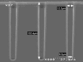
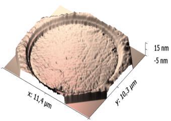
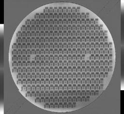
9 Process flow for interposer Example of Leti-Shinko High Density interposer <<< << Total size: 26x26mm, Thickness 100µm Micro Copper bumps: Pitch 50µm, /interposer Damascene: 2 line and 1 via levels, CDmin 0.5µm TSV: 10x100µm RDL and passivation: CDmin 10µm High pillars: pitch 500µm, height TSV SUMMIT N.Sillon 9

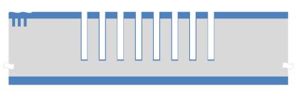

10 Process flow description: front side TSV etching TSV insulation TSV and line 1 metallization Damascene levels Micro bumps Temporary bonding TSV SUMMIT N.Sillon 10


11 Process flow description: back side Back side thinning and TSV exposure Backside Redistribution Layer Backside passivation and High Pillars Debonding TSV SUMMIT N.Sillon 11


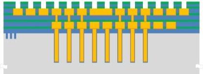
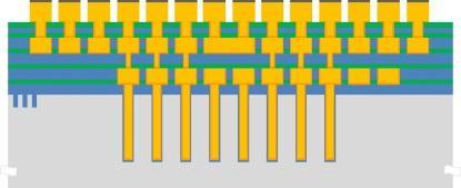
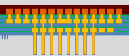
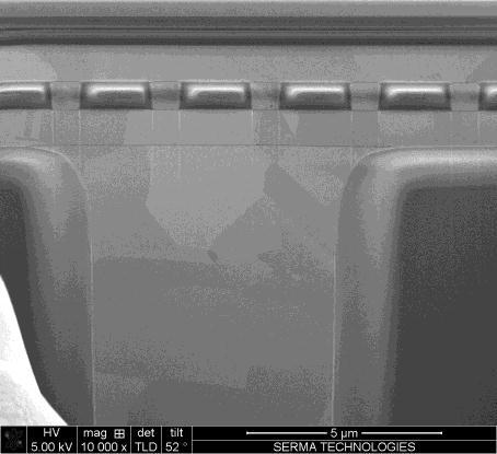
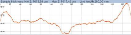
12 Physical characterisation: cross section Good integrity of the overall structure: no delamination No copper extrusion or residue between TSV and Line 1 No copper extrusion or residue between TSV and Backside RDL TSV SUMMIT N.Sillon 12

")

13 Process flow description: Assembly Silicon interposer After mounting (4chip, Si-IP, Organic substrate) Silicon interposer chip chip Organic substrate TSV SUMMIT N.Sillon 13


14 On Going Developments BOW/Constraint management Dev. of low stress BEOL Insertion of compensation layers TSV SUMMIT N.Sillon 14
15 On Going Developments BOW/Constraint management Underfill materials for high troughput CTE mismatch compensation between organic substrate and Silicon Interposer Evolution towards Silicon Package TSV SUMMIT N.Sillon 15
16 Agenda Introduction 2,5D: Silicon Interposer 3DIC: Wide I/O Memory-On-Logic 3D Packaging: X-Ray sensor Conclusion TSV SUMMIT N.Sillon 16


17 3D ST-Leti: from Lab to Fab Prototyping/Production Industrial maturity and stability Short Cycle time 2 complementary Lines Maturity Advanced Dev Advanced flows Advanced demonstrators Benchmark tools Design Teams STE/STM/Leti Advanced modules


 Partitioning")


18 3D Integration successes Leti-STMicro ST implement TSV for CMOS image sensors in 300mm (Process from Leti) Partitioning 45nm/130 nm Demonstrator (Set Top Box application) 300mm R&D Line for 3D Leti Wide I/O Memory + Logic stack. Partitioning Analog/Logic Demonstrator. HDMI Product


19 Wide I/O DRAM stacking on Logic Objectives SoC in advanced CMOS node Quad-channel Wide I/O DRAM* Bandwidth >10GByte/s Reduced power consumption Face to back 3D integration Top die: μ-bumps Bottom die: Bumps, TSV & μ-pillars Die-to-die stacking on BGA * JEDEC standard JESD229 TSV SUMMIT N.Sillon 19


20 Wide I/O : Design Channel 0 Channel 1 Bank 0 Bank 1 Bank 0 Bank 1 Bank 2 Bank n Bank 2 Bank n Bank 0 Bank 1 Bank 0 Bank 1 Bank 2 Bank n Bank 2 Bank n Design STE/Leti Mag3D platform: Low power, NoC based architecture Channel 2 Channel 3 Commercial memory Wide-IO memory: Power efficient and high bandwidth TSV SUMMIT N.Sillon 20


21 3D ST-Leti: from Lab to Fab Temporary Bonding/debonding Back side TSV reveal Si Cu SiO 2 SiO 2 /Ta Advanced modules Micro pillar


22 3D ST-Leti: from Lab to Fab Wide I/O Daisy Chain Maturity Advanced Dev Advanced flows Advanced demonstrators Benchmark tools No TSV leakage Advanced modules > 98% yield on TSV chain
23 3D ST-Leti: from Lab to Fab Prototyping/Production Industrial maturity and stability Short Cycle time WIDE IO DRAM Maturity Advanced Dev Wide I/O demonstrator CuNiAu µ-pillar SoC TSV Advanced flows Advanced demonstrators Benchmark tools Bump Advanced modules BGA
![Memory on Application Processor Wioming SoC [1], co-designed by CEA / ST-Ericsson 73 mm 2,](/docs-images/73/68128871/images/24-2.jpg "1250 TSV and ~1000 Bumps Bottom / BGA Wide I/O DRAM 1GB, 4x128 bits, 200MHz 3D Process and")


24 Memory on Application Processor Wioming SoC [1], co-designed by CEA / ST-Ericsson 73 mm 2, 1250 TSV and ~1000 Bumps Bottom / BGA Wide I/O DRAM 1GB, 4x128 bits, 200MHz 3D Process and test performed in Grenoble Wioming SoC floorplan WIDE IO DRAM SoC WIDE IO DRAM CuNiAu µ-pillar SoC TSV Full functionality demonstrated with high final test yield Performances exceed JEDEC Wide IO standard Bandwidth Power consumption Bump BGA TSV SUMMIT N.Sillon 24 [1] A Three-Layers 3D-IC Stack including Wide IO and a 3D NoC - a Practical Design Perspective P. Vivet & al, RTI 2011
25 Agenda Introduction 2,5D: Silicon Interposer 3DIC: Wide I/O Memory-On-Logic 3D Packaging: : X-Ray sensor Conclusion TSV SUMMIT N.Sillon 25
26 Open 3D: starting point TSV / 3D can be a solution for a lot of devices, whatever the reason (compacity, heterogeneity, cost, performance ) A complete 3D development is long and costly (techno developement, specific design, ). Mature/flexible technologies can be used for low cost demonstrators TSV SUMMIT N.Sillon 26


27 Open 3D : Boost 3D diffusion in applications Our goal: facilitate access to 3D technology Need 3D on your wafers? Open 3D TechBox 3D Design & Layout 3D Technology 3D Packaging

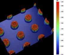
28 First success story : Open 3D for CERN high spatial, high contrast resolving CMOS pixel read-out chip working in single photon counting mode It can be combined with different semiconductor sensors which convert the X- rays directly into detectable electric signals. This represents a new solution for various X- ray and gamma-ray imaging applications. Project started On June 2011 First wafers delivered on January 2012 TSV TSV SUMMIT N.Sillon 28


29 First success story : Open 3D for CERN Design Test structures Process Flow Wafer view Single chip Technology RDL Back side UBM Medipix wafer after front side UBM Accoustic image of the bonding interface TSV Thin wafer on tape TSV SUMMIT N.Sillon 29


30 % First success story : Open 3D for CERN Contact UBM Wafer level Electrical Tests Functionnal tests on ASICS P01-Résistance cumulée Chaine de 2 TSV (VSS) TSV 2 TSV chain resistance Test RDL Test Final E E E E E E E -01 Ohms Chip Delivery & test GELPAK of 16 diced chips Test Board & socket (Courtesy of Jerome ALOZY / CERN) TSV SUMMIT N.Sillon 30
 Next step:")
31 1 1 First success story : Open 3D for CERN W24-H2 DAC dependency (Courtesy of Jerome ALOZY / CERN) Next step: Integration
32 Conclusion We have in mind complete 3D integrated systems with intermediate products. Concrete 3D integrations demonstrators have been achieved with partners, allowing low capex validation and anticipation of integration problems for manufacturing Silicon Interposer 3D IC memory on logic Xray Detector Toolbox development is still on going for next gen with tools/materials suppliers TSV SUMMIT N.Sillon 32
33 Warm Thanks to all 3D community TSV SUMMIT N.Sillon 33

34 Merci de votre attention TSV SUMMIT N.Sillon 34
3D technology evolution to smart interposer and high density 3D ICs
 3D technology evolution to smart interposer and high density 3D ICs Patrick Leduc, Jean Charbonnier, Nicolas Sillon, Séverine Chéramy, Yann Lamy, Gilles Simon CEA-Leti, Minatec Campus Why 3D integration?
3D TECHNOLOGIES: SOME PERSPECTIVES FOR MEMORY INTERCONNECT AND CONTROLLER
 3D TECHNOLOGIES: SOME PERSPECTIVES FOR MEMORY INTERCONNECT AND CONTROLLER CODES+ISSS: Special session on memory controllers Taipei, October 10 th 2011 Denis Dutoit, Fabien Clermidy, Pascal Vivet {denis.dutoit@cea.fr}
Bringing 3D Integration to Packaging Mainstream
 Bringing 3D Integration to Packaging Mainstream Enabling a Microelectronic World MEPTEC Nov 2012 Choon Lee Technology HQ, Amkor Highlighted TSV in Packaging TSMC reveals plan for 3DIC design based on silicon
TSV : impact on microelectronics European 3D TSV Summit MINATEC Campus Grenoble, January 22nd, 2013
 TSV : impact on microelectronics European 3D TSV Summit MINATEC Campus Grenoble, January 22nd, 2013 Welcome in Grenoble Grenoble : 3D by Nature Pour modifier: Insertion / En Tête/Pied de page -Titre de
3D SYSTEM INTEGRATION TECHNOLOGY CHOICES AND CHALLENGE ERIC BEYNE, ANTONIO LA MANNA
 3D SYSTEM INTEGRATION TECHNOLOGY CHOICES AND CHALLENGE ERIC BEYNE, ANTONIO LA MANNA OUTLINE 3D Application Drivers and Roadmap 3D Stacked-IC Technology 3D System-on-Chip: Fine grain partitioning Conclusion
TechSearch International, Inc.
 Silicon Interposers: Ghost of the Past or a New Opportunity? Linda C. Matthew TechSearch International, Inc. www.techsearchinc.com Outline History of Silicon Carriers Thin film on silicon examples Multichip
L évolution des architectures et des technologies d intégration des circuits intégrés dans les Data centers
 I N S T I T U T D E R E C H E R C H E T E C H N O L O G I Q U E L évolution des architectures et des technologies d intégration des circuits intégrés dans les Data centers 10/04/2017 Les Rendez-vous de
Interposer Technology: Past, Now, and Future
 Interposer Technology: Past, Now, and Future Shang Y. Hou TSMC 侯上勇 3D TSV: Have We Waited Long Enough? Garrou (2014): A Little More Patience Required for 2.5/3D All things come to those who wait In 2016,
3D SoC and Heterogeneous Integrations
 3D SoC and Heterogeneous Integrations Content Introduction ST positioning Why 3D-Integration? CMOS Imager Sensor: the TSV success story! 3D SOC technology & applications Via Middle FE integrations Back-side
Stacked Silicon Interconnect Technology (SSIT)
") Stacked Silicon Interconnect Technology (SSIT) Suresh Ramalingam Xilinx Inc. MEPTEC, January 12, 2011 Agenda Background and Motivation Stacked Silicon Interconnect Technology Summary Background and Motivation
Stacked Silicon Interconnect Technology (SSIT) Suresh Ramalingam Xilinx Inc. MEPTEC, January 12, 2011 Agenda Background and Motivation Stacked Silicon Interconnect Technology Summary Background and Motivation
Comparison & highlight on the last 3D TSV technologies trends Romain Fraux
 Comparison & highlight on the last 3D TSV technologies trends Romain Fraux Advanced Packaging & MEMS Project Manager European 3D Summit 18 20 January, 2016 Outline About System Plus Consulting 2015 3D
EECS 598: Integrating Emerging Technologies with Computer Architecture. Lecture 10: Three-Dimensional (3D) Integration
 Integration") 1 EECS 598: Integrating Emerging Technologies with Computer Architecture Lecture 10: Three-Dimensional (3D) Integration Instructor: Ron Dreslinski Winter 2016 University of Michigan 1 1 1 Announcements
1 EECS 598: Integrating Emerging Technologies with Computer Architecture Lecture 10: Three-Dimensional (3D) Integration Instructor: Ron Dreslinski Winter 2016 University of Michigan 1 1 1 Announcements
Advancing high performance heterogeneous integration through die stacking
 Advancing high performance heterogeneous integration through die stacking Suresh Ramalingam Senior Director, Advanced Packaging European 3D TSV Summit Jan 22 23, 2013 The First Wave of 3D ICs Perfecting
Wafer Level Packaging The Promise Evolves Dr. Thomas Di Stefano Centipede Systems, Inc. IWLPC 2008
 Wafer Level Packaging The Promise Evolves Dr. Thomas Di Stefano Centipede Systems, Inc. IWLPC 2008 / DEVICE 1.E+03 1.E+02 1.E+01 1.E+00 1.E-01 1.E-02 1.E-03 1.E-04 1.E-05 1.E-06 1.E-07 Productivity Gains
WLSI Extends Si Processing and Supports Moore s Law. Douglas Yu TSMC R&D,
 WLSI Extends Si Processing and Supports Moore s Law Douglas Yu TSMC R&D, chyu@tsmc.com SiP Summit, Semicon Taiwan, Taipei, Taiwan, Sep. 9 th, 2016 Introduction Moore s Law Challenges Heterogeneous Integration
THERMAL EXPLORATION AND SIGN-OFF ANALYSIS FOR ADVANCED 3D INTEGRATION
 THERMAL EXPLORATION AND SIGN-OFF ANALYSIS FOR ADVANCED 3D INTEGRATION Cristiano Santos 1, Pascal Vivet 1, Lee Wang 2, Michael White 2, Alexandre Arriordaz 3 DAC Designer Track 2017 Pascal Vivet Jun/2017
TechSearch International, Inc.
 On the Road to 3D ICs: Markets and Solutions E. Jan Vardaman President TechSearch International, Inc. www.techsearchinc.com High future cost of lithography Severe interconnect delay Noted in ITRS roadmap
Multi-Die Packaging How Ready Are We?
 Multi-Die Packaging How Ready Are We? Rich Rice ASE Group April 23 rd, 2015 Agenda ASE Brief Integration Drivers Multi-Chip Packaging 2.5D / 3D / SiP / SiM Design / Co-Design Challenges: an OSAT Perspective
Keynote Speaker. Matt Nowak Senior Director Advanced Technology Qualcomm CDMA Technologies
 Keynote Speaker Emerging High Density 3D Through Silicon Stacking (TSS) What s Next? Matt Nowak Senior Director Advanced Technology Qualcomm CDMA Technologies 8 Emerging High Density 3D Through Silicon
3DIC & TSV interconnects
 3DIC & TSV interconnects 2012 Business update Semicon Taiwan 2012 baron@yole.fr Infineon VTI Xilinx Synopsys Micron CEA LETI 2012 Copyrights Yole Developpement SA. All rights reserved. Semiconductor chip
Physical Design Implementation for 3D IC Methodology and Tools. Dave Noice Vassilios Gerousis
 I NVENTIVE Physical Design Implementation for 3D IC Methodology and Tools Dave Noice Vassilios Gerousis Outline 3D IC Physical components Modeling 3D IC Stack Configuration Physical Design With TSV Summary
Thermal Sign-Off Analysis for Advanced 3D IC Integration
 Sign-Off Analysis for Advanced 3D IC Integration Dr. John Parry, CEng. Senior Industry Manager Mechanical Analysis Division May 27, 2018 Topics n Acknowledgements n Challenges n Issues with Existing Solutions
Advanced Packaging For Mobile and Growth Products
 Advanced Packaging For Mobile and Growth Products Steve Anderson, Senior Director Product and Technology Marketing, STATS ChipPAC Growing Needs for Silicon & Package Integration Packaging Trend Implication
There is a paradigm shift in semiconductor industry towards 2.5D and 3D integration of heterogeneous parts to build complex systems.
 Direct Connection and Testing of TSV and Microbump Devices using NanoPierce Contactor for 3D-IC Integration There is a paradigm shift in semiconductor industry towards 2.5D and 3D integration of heterogeneous
TechSearch International, Inc.
 Alternatives on the Road to 3D TSV E. Jan Vardaman President TechSearch International, Inc. www.techsearchinc.com Everyone Wants to Have 3D ICs 3D IC solves interconnect delay problem bandwidth bottleneck
SMAFTI Package Technology Features Wide-Band and Large-Capacity Memory
 SMAFTI Package Technology Features Wide-Band and Large-Capacity Memory KURITA Yoichiro, SOEJIMA Koji, KAWANO Masaya Abstract and NEC Corporation have jointly developed an ultra-compact system-in-package
DEPARTMENT WAFER LEVEL SYSTEM INTEGRATION
 FRAUNHOFER INSTITUTE FOR RELIABILITY AND MICROINTEGRATION IZM DEPARTMENT WAFER LEVEL SYSTEM INTEGRATION ALL SILICON SYSTEM INTEGRATION DRESDEN ASSID ALL SILICON SYSTEM INTEGRATION DRESDEN FRAUNHOFER IZM-ASSID
Technology and Manufacturing
 Technology and Manufacturing Executive Vice President Field Trip 2006 - London, May 23rd Field Trip 2006 - London, May 23rd Technology Technology Development Centers and Main Programs CMOS Logic Platform
3D technology for Advanced Medical Devices Applications
 3D technology for Advanced Medical Devices Applications By, Dr Pascal Couderc,Jerome Noiray, Dr Christian Val, Dr Nadia Boulay IMAPS MEDICAL WORKSHOP DECEMBER 4 & 5,2012 P.COUDERC 3D technology for Advanced
Material technology enhances the density and the productivity of the package
 Material technology enhances the density and the productivity of the package May 31, 2018 Toshihisa Nonaka, Ph D. Packaging Solution Center Advanced Performance Materials Business Headquarter Hitachi Chemical
Challenges of Integration of Complex FHE Systems. Nancy Stoffel GE Global Research
 Challenges of Integration of Complex FHE Systems Nancy Stoffel GE Global Research Products drive requirements to sub-systems, components and electronics GE PRODUCTS CTQs: SWaP, $$, operating environment,
3-D Package Integration Enabling Technologies
 3-D Package Integration Enabling Technologies Nanium - Semi Networking Day David Clark - Choon Heung Lee - Ron Huemoeller June 27th, 2013 Enabling a Microelectronic World Mobile Communications Driving
DFT-3D: What it means to Design For 3DIC Test? Sanjiv Taneja Vice President, R&D Silicon Realization Group
 I N V E N T I V E DFT-3D: What it means to Design For 3DIC Test? Sanjiv Taneja Vice President, R&D Silicon Realization Group Moore s Law & More : Tall And Thin More than Moore: Diversification Moore s
3D Integration & Packaging Challenges with through-silicon-vias (TSV)
") NSF Workshop 2/02/2012 3D Integration & Packaging Challenges with through-silicon-vias (TSV) Dr John U. Knickerbocker IBM - T.J. Watson Research, New York, USA Substrate IBM Research Acknowledgements IBM
NSF Workshop 2/02/2012 3D Integration & Packaging Challenges with through-silicon-vias (TSV) Dr John U. Knickerbocker IBM - T.J. Watson Research, New York, USA Substrate IBM Research Acknowledgements IBM
3D INTEGRATION, A SMART WAY TO ENHANCE PERFORMANCE. Leti Devices Workshop December 3, 2017
 3D INTEGRATION, A SMART WAY TO ENHANCE PERFORMANCE OVERAL GOAL OF THIS TALK Hybrid bonding 3D sequential 3D VLSI technologies (3D VIA Pitch
Opportunities & Challenges: 28nm & 2.5/3-D IC Design and Manufacturing
 Opportunities & Challenges: 28nm & 2.5/3-D IC Design and Manufacturing Vincent Tong Senior Vice President & Asia Pacific Executive Leader Copyright 2011 Xilinx Agenda Xilinx Business Drivers All in at
High Volume Manufacturing Supply Chain Ecosystem for 2.5D HBM2 ASIC SiPs
 Open-Silicon.com 490 N. McCarthy Blvd, #220 Milpitas, CA 95035 408-240-5700 HQ High Volume Manufacturing Supply Chain Ecosystem for 2.5D HBM2 ASIC SiPs Open-Silicon Asim Salim VP Mfg. Operations 20+ experience
Xilinx SSI Technology Concept to Silicon Development Overview
 Xilinx SSI Technology Concept to Silicon Development Overview Shankar Lakka Aug 27 th, 2012 Agenda Economic Drivers and Technical Challenges Xilinx SSI Technology, Power, Performance SSI Development Overview
Advanced CSP & Turnkey Solutions. Fumio Ohyama Tera Probe, Inc.
 Advanced CSP & Turnkey Solutions Fumio Ohyama Tera Probe, Inc. Tera Probe - Corporate Overview 1. Company : Tera Probe, Inc. 2. Founded : August, 2005 3. Capital : Approx. USD118.2 million (as of March
Packaging Technology for Image-Processing LSI
 Packaging Technology for Image-Processing LSI Yoshiyuki Yoneda Kouichi Nakamura The main function of a semiconductor package is to reliably transmit electric signals from minute electrode pads formed on
3DIC & TSV interconnects business update
 3DIC & TSV interconnects business update ASET presentation. Infineon VTI Xilinx Synopsys Micron CEA LETI 2012 Copyrights Yole Developpement SA. All rights reserved. Fields of Expertise Yole Developpement
Non-destructive, High-resolution Fault Imaging for Package Failure Analysis. with 3D X-ray Microscopy. Application Note
 Non-destructive, High-resolution Fault Imaging for Package Failure Analysis with 3D X-ray Microscopy Application Note Non-destructive, High-resolution Fault Imaging for Package Failure Analysis with 3D
Emerging IC Packaging Platforms for ICT Systems - MEPTEC, IMAPS and SEMI Bay Area Luncheon Presentation
 Emerging IC Packaging Platforms for ICT Systems - MEPTEC, IMAPS and SEMI Bay Area Luncheon Presentation Dr. Li Li Distinguished Engineer June 28, 2016 Outline Evolution of Internet The Promise of Internet
Packaging Innovation for our Application Driven World
 Packaging Innovation for our Application Driven World Rich Rice ASE Group March 14 th, 2018 MEPTEC / IMAPS Luncheon Series 1 What We ll Cover Semiconductor Roadmap Drivers Package Development Thrusts Collaboration
Introduction. SK hynix
 It was very informative. I had a lot of questions answered. It was a good assembly of design and manufacturing elements. I learned a lot that I didn t know. It s good to hear that TSVs are ready for HBM.
2.5D interposer, 3DIC and TSV Interconnects Applications, market trends and supply chain evolutions
 2.5D interposer, 3DIC and TSV Interconnects Applications, market trends and supply chain evolutions Dr Lionel Cadix cadix@yole.fr CEA LETI Infineon VTI Synopsys Xilinx Micron 2012 Outline Introduction
Heterogeneous Integration and the Photonics Packaging Roadmap
 Heterogeneous Integration and the Photonics Packaging Roadmap Presented by W. R. Bottoms Packaging Photonics for Speed & Bandwidth The Functions Of A Package Protect the contents from damage Mechanical
Photonics Integration in Si P Platform May 27 th Fiber to the Chip
 Photonics Integration in Si P Platform May 27 th 2014 Fiber to the Chip Overview Introduction & Goal of Silicon Photonics Silicon Photonics Technology Wafer Level Optical Test Integration with Electronics
Comparison of Singulation Techniques
 Comparison of Singulation Techniques Electronic Packaging Society, Silicon Valley Chapter Sept. 28, 2017 ANNETTE TENG Sept 28, 2017 1 Definition of Singulation 9/28/2017 Annetteteng@promex-ind.com 2 www.cpmt.org/scv
3D Hetero-Integration Technology for Future Automotive Smart Vehicle System
 3D Hetero-Integration Technology for Future Automotive Smart Vehicle System Kangwook Lee, Ph.D Professor, NICHe, Tohoku University Deputy Director, Global INTegration Initiative (GINTI) Kangwook Lee, Tohoku
Photonics & 3D, Convergence Towards a New Market Segment Eric Mounier Thibault Buisson IRT Nanoelec, Grenoble, 21 mars 2016
 From Technologies to Market Photonics & 3D, Convergence Towards a New Market Segment Eric Mounier Thibault Buisson IRT Nanoelec, Grenoble, 21 mars 2016 2016 CONTENT Silicon Photonics value proposition
Vertical Circuits. Small Footprint Stacked Die Package and HVM Supply Chain Readiness. November 10, Marc Robinson Vertical Circuits, Inc
 Small Footprint Stacked Die Package and HVM Supply Chain Readiness Marc Robinson Vertical Circuits, Inc November 10, 2011 Vertical Circuits Building Blocks for 3D Interconnects Infrastructure Readiness
Advanced Heterogeneous Solutions for System Integration
 Advanced Heterogeneous Solutions for System Integration Kees Joosse Director Sales, Israel TSMC High-Growth Applications Drive Product and Technology Smartphone Cloud Data Center IoT CAGR 12 17 20% 24%
3D-IC is Now Real: Wide-IO is Driving 3D-IC TSV. Samta Bansal and Marc Greenberg, Cadence EDPS Monterey, CA April 5-6, 2012
 3D-IC is Now Real: Wide-IO is Driving 3D-IC TSV Samta Bansal and Marc Greenberg, Cadence EDPS Monterey, CA April 5-6, 2012 What the fuss is all about * Source : ECN Magazine March 2011 * Source : EDN Magazine
From Advanced Package to 2.5D/3D IC. Amkor Technology : Choon Lee
 From Advanced Package to 2.5D/3D IC Amkor Technology : Choon Lee History says Low pin High pin & Integration As Multi-function pager City phone / PCS Feature Phone Smart Phone SOIC QFP PBGA Package-on-Package
Embedded UTCP interposers for miniature smart sensors
 Embedded UTCP interposers for miniature smart sensors T. Sterken 1,2, M. Op de Beeck 2, Tom Torfs 2, F. Vermeiren 1,2, C. Van Hoof 2, J. Vanfleteren 1,2 1 CMST (affiliated with Ugent and IMEC), Technologiepark
New Era of Panel Based Technology for Packaging, and Potential of Glass. Shin Takahashi Technology Development General Division Electronics Company
 New Era of Panel Based Technology for Packaging, and Potential of Glass Shin Takahashi Technology Development General Division Electronics Company Connecting the World Connecting the World Smart Mobility
Ultra-thin Capacitors for Enabling Miniaturized IoT Applications
 Ultra-thin Capacitors for Enabling Miniaturized IoT Applications Fraunhofer Demo Day, Oct 8 th, 2015 Konrad Seidel, Fraunhofer IPMS-CNT 10/15/2015 1 CONTENT Why we need thin passive devices? Integration
Japanese two Samurai semiconductor ventures succeeded in near 3D-IC but failed the business, why? and what's left?
 Japanese two Samurai semiconductor ventures succeeded in near 3D-IC but failed the business, why? and what's left? Liquid Design Systems, Inc CEO Naoya Tohyama Overview of this presentation Those slides
Packaging for parallel optical interconnects with on-chip optical access
 Packaging for parallel optical interconnects with on-chip optical access I. INTRODUCTION Parallel optical interconnects requires the integration of lasers and detectors directly on the CMOS chip. In the
IMEC CORE CMOS P. MARCHAL
 APPLICATIONS & 3D TECHNOLOGY IMEC CORE CMOS P. MARCHAL OUTLINE What is important to spec 3D technology How to set specs for the different applications - Mobile consumer - Memory - High performance Conclusions
Update: Lambda project
 Update: Lambda project Sabine Lange Detector Group DESY meeting, May 29-31, 2012 s1 Lambda project About Lambda: 2 x 6 3 chips (~28 x 85mm) high frame rate (8 read out lines, 2kHz readout) 10 gigabit Ethernet
ARCHIVE Françoise von Trapp Editorial Director 3D InCites ABSTRACT
 2010 Invited Speaker ARCHIVE 2010 RISING TO THE 3D TSV TEST CHALLENGE: WILL YOU BE READY? by Françoise von Trapp Editorial Director 3D InCites 3D ABSTRACT integration is not a novel concept. Veterans in
High speed full wafer monitoring of surface, edge and bonding interface for 3D-stacking
 Sematech Workshop on 3D Interconnect Metrology Sematech Workshop on 3D Interconnect Metrology, July 13 2011 High speed full wafer monitoring of surface, edge and bonding interface for 3D-stacking Lars
Interconnect Challenges in a Many Core Compute Environment. Jerry Bautista, PhD Gen Mgr, New Business Initiatives Intel, Tech and Manuf Grp
 Interconnect Challenges in a Many Core Compute Environment Jerry Bautista, PhD Gen Mgr, New Business Initiatives Intel, Tech and Manuf Grp Agenda Microprocessor general trends Implications Tradeoffs Summary
Development of innovative ALD materials for high density 3D integrated capacitors
 Development of innovative ALD materials for high density 3D integrated capacitors Malte Czernohorsky General Trend: System miniaturization Integration of passive components Capacitors Inductors Resistors
OPTICAL TECHNOLOGIES FOR TSV INSPECTION Arun A. Aiyer, Frontier Semiconductor 2127 Ringwood Ave, San Jose, California 95131
 OPTICAL TECHNOLOGIES FOR TSV INSPECTION Arun A. Aiyer, Frontier Semiconductor 2127 Ringwood Ave, San Jose, California 95131 ABSTRACT: In this paper, Frontier Semiconductor will introduce a new technology
Burn-in & Test Socket Workshop
 Burn-in & Test Socket Workshop IEEE March 4-7, 2001 Hilton Mesa Pavilion Hotel Mesa, Arizona IEEE COMPUTER SOCIETY Sponsored By The IEEE Computer Society Test Technology Technical Council COPYRIGHT NOTICE
Packaging of Selected Advanced Logic in 2x and 1x nodes. 1 I TechInsights
 Packaging of Selected Advanced Logic in 2x and 1x nodes 1 I TechInsights Logic: LOGIC: Packaging of Selected Advanced Devices in 2x and 1x nodes Xilinx-Kintex 7XC 7 XC7K325T TSMC 28 nm HPL HKMG planar
Beyond Chip Stacking---Quilt Packaging Enabled 3D Systems
 Beyond Chip Stacking---Quilt Packaging Enabled 3D Systems Jason Kulick, President & Co-Founder jason.kulick@indianaic.com 574-217-4612 (South Bend, IN) May 3, 2016 2016 New England IMAPS Symposium Presentation
Technology Platform Segmentation
 HOW TECHNOLOGY R&D LEADERSHIP BRINGS A COMPETITIVE ADVANTAGE FOR MULTIMEDIA CONVERGENCE Technology Platform Segmentation HP LP 2 1 Technology Platform KPIs Performance Design simplicity Power leakage Cost
Three Dimensional Integration
 Three Dimensional Integration Paul Franzon North Carolina State University Raleigh, NC paulf@ncsu.edu 919.515.7351 Outline 3DIC Motivation Performance and Memory Bandwidth Power Efficiency Power per unit
3D Embedded Multi-core: Some Perspectives
 3D Embedded Multi-core: Some Perspectives Fabien Clermidy, Florian Darve, Denis Dutoit, Walid Lafi, Pascal Vivet CEA-LETI, Minatec Campus, 38054 Grenoble, FRANCE {firstname.lastname@cea.fr} Abstract 3D
The Evolution of Multi-Chip Packaging: from MCMs to 2.5/3D to Photonics. David McCann November 14, 2016
 The Evolution of Multi-Chip Packaging: from MCMs to 2.5/3D to Photonics David McCann November 14, 2016 Outline Multi-Chip Module Evolution We had MCM s. What Happened? What Have we Learned? Trends and
Embedded Power Dies for System-in-Package (SiP)
") Embedded Power Dies for System-in-Package (SiP) D. Manessis, L. Boettcher, S. Karaszkiewicz, R.Patzelt, D. Schuetze, A. Podlasky, A. Ostmann Fraunhofer Institute for Reliability and Microintegration (IZM),
Embedded Power Dies for System-in-Package (SiP) D. Manessis, L. Boettcher, S. Karaszkiewicz, R.Patzelt, D. Schuetze, A. Podlasky, A. Ostmann Fraunhofer Institute for Reliability and Microintegration (IZM),
Probing 25µm-diameter micro-bumps for Wide-I/O 3D SICs
 The International Magazine for the Semiconductor Packaging Industry Volume 18, Number 1 January February 2014 Probing 25µm-diameter micro-bumps for Wide-I/O 3D SICs Page 20 3D ICs The future of interposers
The Foundry-Packaging Partnership. Enabling Future Performance. Jon A. Casey. IBM Systems and Technology Group
 The Foundry-Packaging Partnership Enabling Future Performance Jon A. Casey IBM Fellow IBM Systems and Technology Group 5/30/2013 2012 IBM Corporation Data growth will drive the new IT model Dimensions
Packaging avancé pour les modules photoniques
 I N S T I T U T D E R E C H E R C H E T E C H N O L O G I Q U E Packaging avancé pour les modules photoniques S. Bernabé, CEA-Leti Marc Epitaux, SAMTEC Workshop «Photonique sur Silicium, une rupture attendue»
Applications for Mapper technology Bert Jan Kampherbeek
 Applications for Mapper technology Bert Jan Kampherbeek Co-founder & CEO Today s agenda Mapper technology Principles of operation Development status and performance Specification summary Mapper applications
SRC 3D Summit. Bob Patti, CTO
 SRC 3D Summit Bob Patti, CTO rpatti@tezzaron.com 1 Advantages Why We Scale? What can 3D do for us? Speed Power Cost Size >180nm 130nm 90nm 65nm 45nm 28nm 22nm 16nm 2 How Real is 3D??? 560μ Samsung 16Gb
Chapter 0 Introduction
 Chapter 0 Introduction Jin-Fu Li Laboratory Department of Electrical Engineering National Central University Jhongli, Taiwan Applications of ICs Consumer Electronics Automotive Electronics Green Power
Monolithic 3D Integration using Standard Fab & Standard Transistors. Zvi Or-Bach CEO MonolithIC 3D Inc.
 Monolithic 3D Integration using Standard Fab & Standard Transistors Zvi Or-Bach CEO MonolithIC 3D Inc. 3D Integration Through Silicon Via ( TSV ), Monolithic Increase integration Reduce interconnect total
High performance HBM Known Good Stack Testing
 High performance HBM Known Good Stack Testing FormFactor Teradyne Overview High Bandwidth Memory (HBM) Market and Technology Probing challenges Probe solution Power distribution challenges PDN design Simulation
Start Your HBM/2.5D Design Today
 Kevin Tran SK hynix Inc. Paul Silvestri Amkor Technology, Inc. Bill Isaacson esilicon Corporation Brian Daellenbach Northwest Logic Chris Browy Avery Design Systems Executive Summary High-bandwidth memory
Beyond Moore. Beyond Programmable Logic.
 Beyond Moore Beyond Programmable Logic Steve Trimberger Xilinx Research FPL 30 August 2012 Beyond Moore Beyond Programmable Logic Agenda What is happening in semiconductor technology? Moore s Law More
ARCHIVE 2008 COPYRIGHT NOTICE
 Keynote Speaker ARCHIVE 2008 Packaging & Assembly in Pursuit of Moore s Law and Beyond Karl Johnson Ph.D. Vice President and Senior Fellow Advanced Packaging Systems Integration Laboratory Freescale Semiconductor
inemi Roadmap Packaging and Component Substrates TWG
 inemi Roadmap Packaging and Component Substrates TWG TWG Leaders: W. R. Bottoms William Chen Presented by M. Tsuriya Agenda Situation Everywhere in Electronics Evolution & Blooming Drivers Changing inemi
2.5D FPGA-HBM Integration Challenges
 2.5D FPGA-HBM Integration Challenges Jaspreet Gandhi, Boon Ang, Tom Lee, Henley Liu, Myongseob Kim, Ho Hyung Lee, Gamal Refai-Ahmed, Hong Shi, Suresh Ramalingam Xilinx Inc., San Jose CA Page 1 Presentation
3D systems-on-chip. A clever partitioning of circuits to improve area, cost, power and performance. The 3D technology landscape
 Edition April 2017 Semiconductor technology & processing 3D systems-on-chip A clever partitioning of circuits to improve area, cost, power and performance. In recent years, the technology of 3D integration
3D & Advanced Packaging
 Tuesday, October 03, 2017 Company Overview March 12, 2015 3D & ADVANCED PACKAGING IS NOW WITHIN REACH WHAT IS NEXT LEVEL INTEGRATION? Next Level Integration blends high density packaging with advanced
Mixed-Signal. From ICs to Systems. Mixed-Signal solutions from Aeroflex Colorado Springs. Standard products. Custom ASICs. Mixed-Signal modules
 A passion for performance. Mixed-Signal solutions from Aeroflex Colorado Springs Standard products Custom ASICs Mixed-Signal modules Circuit card assemblies Mixed-Signal From ICs to Systems RadHard ASICs
Soitec ultra-thin SOI substrates enabling FD-SOI technology. July, 2015
 Soitec ultra-thin SOI substrates enabling FD-SOI technology July, 2015 Agenda FD-SOI: Background & Value Proposition C1- Restricted July 8, 2015 2 Today Ultra-mobile & Connected Consumer At Any Time With
>Introduction Ibiden Products Over View and Technology Trend. Embedding technology and Expectation.
 Agenda >Introduction Ibiden Products Over View and Technology Trend. Embedding technology and Expectation. >Embedded Device Technology #1. Embedded MLCC in FCCSP Substrate. #2. Embedded Active Device.
INDUSTRY REVIEW FOCUS ON MEMS PACKAGING. Two very different approaches to MEMS packaging
 F e b r u a r y 2 0 1 3 I S S U E N 2 6 Packaging beyond the mainstream By 3D Packaging Editorial Team Emerging volume markets in MEMS, LEDs, power devices and even silicon photonics mean an increasing
Total Inspection Solutions Ensuring Known-Good 3DIC Package. Nevo Laron, Camtek USA, Santa Clara, CA
 Total Inspection Solutions Ensuring Known-Good 3DIC Package Nevo Laron, Camtek USA, Santa Clara, CA Density Packaging Trends vs. Defect Costs Functionality Package Yield 3DIC yield statistics 101 1.00
Non-contact Test at Advanced Process Nodes
 Chris Sellathamby, J. Hintzke, B. Moore, S. Slupsky Scanimetrics Inc. Non-contact Test at Advanced Process Nodes June 8-11, 8 2008 San Diego, CA USA Overview Advanced CMOS nodes are a challenge for wafer
3D Integration: New Opportunities for Speed, Power and Performance. Robert Patti, CTO
 3D Integration: New Opportunities for Speed, Power and Performance Robert Patti, CTO rpatti@tezzaron.com 1 Advantages Why We Scale? What can 3D do for us? Speed Power Cost Size >180nm 130nm 90nm 65nm 45nm
Pushing the Boundaries of Moore's Law to Transition from FPGA to All Programmable Platform Ivo Bolsens, SVP & CTO Xilinx ISPD, March 2017
 Pushing the Boundaries of Moore's Law to Transition from FPGA to All Programmable Platform Ivo Bolsens, SVP & CTO Xilinx ISPD, March 2017 High Growth Markets Cloud Computing Automotive IIoT 5G Wireless
Thermal Management Challenges in Mobile Integrated Systems
 Thermal Management Challenges in Mobile Integrated Systems Ilyas Mohammed March 18, 2013 SEMI-THERM Executive Briefing Thermal Management Market Visions & Strategies, San Jose CA Contents Mobile computing
An integrated solution for KGD: At-speed wafer-level testing and full-contact wafer-level burn-in after flip chip bumping
 An integrated solution for KGD: At-speed wafer-level testing and full-contact wafer-level burn-in after flip chip bumping Yuan-Ping Tseng/ An-Hong Liu TD center ChipMOS Technologies Inc. June 5, 2001 1