KC705 PCIe Design Creation with Vivado August 2012
|
|
|
- Grace Goodman
- 6 years ago
- Views:
Transcription


1 KC705 PCIe Design Creation with Vivado August 2012 XTP197
2 Revision History Date Version Description 08/20/ Initial version. Added AR Copyright 2012 Xilinx, Inc. All Rights Reserved. XILINX, the Xilinx logo, the Brand Window and other designated brands included herein are trademarks of Xilinx, Inc. All other trademarks are the property of their respective owners. NOTICE OF DISCLAIMER: The information disclosed to you hereunder (the Information ) is provided AS-IS with no warranty of any kind, express or implied. Xilinx does not assume any liability arising from your use of the Information. You are responsible for obtaining any rights you may require for your use of this Information. Xilinx reserves the right to make changes, at any time, to the Information without notice and at its sole discretion. Xilinx assumes no obligation to correct any errors contained in the Information or to advise you of any corrections or updates. Xilinx expressly disclaims any liability in connection with technical support or assistance that may be provided to you in connection with the Information. XILINX MAKES NO OTHER WARRANTIES, WHETHER EXPRESS, IMPLIED, OR STATUTORY, REGARDING THE INFORMATION, INCLUDING ANY WARRANTIES OF MERCHANTABILITY, FITNESS FOR A PARTICULAR PURPOSE, OR NONINFRINGEMENT OF THIRD-PARTY RIGHTS.
3 Note: This presentation applies to the KC705 Overview Kintex-7 PCIe x8 Gen 2 Capability Xilinx KC705 Board Software Requirements KC705 Setup Compile PCIe Cores Generate x8 Gen 2 PCIe Core and MCS File Program KC705 Flash with PCIe Design Running the PCIe x8 Gen 2 Design References IP Release Notes Guide XTP025
4 Kintex-7 PCIe x8 Gen 2 Capability KC705 Supports PCIe Gen 1 and Gen 2 Capability x8, x4, x2, or x1 Gen 1 and Gen 2 lane width x8 Gen 2 not supported in -1 parts See DS821 for details LogiCORE PIO Example Design RDF0187.zip Available through LogiCORE Integrated Block for PCI Express See UG477 for details
5 Kintex-7 PCIe x8 Gen 2 Capability Integrated Block for PCI Express PCI Express Base 2.0 Specification Configurable for Endpoint or Root Port Applications KC705 configured for Endpoint Applications GTX Transceivers implement a fully compliant PHY Large range of maximum payload size 128 / 256 / 512 / 1024 bytes Configurable BAR spaces Up to 6 x 32 bit, 3 x 64 bit, or a combination Memory or IO BAR and ID filtering Management and Statistics Interface


6 Xilinx KC705 Board Note: Presentation applies to the KC705

7 ISE Software Requirements Xilinx Vivado software Apply AR50886

8 PciTree Software Requirement PciTree Bus Viewer Free download HLP.SYS must be copied to C:\WINDOWS\system32\drivers directory

9 Generate x8 Gen 2 PCIe Core Open Vivado Start All Programs Xilinx Design Tools Vivado Vivado Select Create New Project
10 Generate x8 Gen 2 PCIe Core Click Next

11 Generate x8 Gen 2 PCIe Core Set the Project name and location to kc705_pcie_vivado and C:\ Check Create Project Subdirectory

12 Generate x8 Gen 2 PCIe Core Select RTL Project Select Do not specify sources at this time

13 Generate x8 Gen 2 PCIe Core Select the KC705 Board
14 Generate x8 Gen 2 PCIe Core Click Finish

15 Generate x8 Gen 2 PCIe Core Click on IP Catalog

16 Generate x8 Gen 2 PCIe Core Select 7 Series PCIe Version 1.6 under Standard Bus Interfaces
17 Generate x8 Gen 2 PCIe Core Right click on 7 Series PCIe Version 1.6 Select Customize IP

18 Note: Pre-built design, RDF0187, available through Generate x8 Gen 2 PCIe Core Under the Page 1 tab, set the Component name to kc705_pcie_x8_ gen2 Set the lane Width to X8 Set the Link Speed to 5 GT/s Set the Frequency to 250 MHz Click on Page 2

19 Generate x8 Gen 2 PCIe Core Under the Page 2 tab, BAR 0 Set to 1 Megabytes Click on Page 3

20 Generate x8 Gen 2 PCIe Core Under the Page 3 tab, note ID Initial Values Vendor ID = 10EE Device ID = 7028 Revision ID = 00 Subsystem Vendor ID = 10EE Subsystem ID = 0007 Click on Page 11

21 Generate x8 Gen 2 PCIe Core Under the Page 11 tab Select KC705 REVC Click on Page 13

22 Generate x8 Gen 2 PCIe Core On Page 13 Set the Reference Clock Freq: 100 MHz Set the Silicon Revision to General ES Click OK
23 Generate x8 Gen 2 PCIe Core PCIe design appears in Design Sources The PCIe IP is already checked but still needs to be generated
24 Compile Example Design Right-click on kc705_pcie_x8_gen2 and select Generate


25 Compile Example Design Select Synthesis, Examples, and Instantiation Template as the targets to generate
26 Compile Example Design Once the Generate step is complete, a check (re)appears on the IP

27 Modify PCIe Core As per AR44635, the design must be modified Open the file: <design path>/<design name>.srcs\sources_1\ip\ kc705_pcie_x8_gen2\kc705_pcie_x8_gen2\example_design\ xilinx_pcie_2_1_ep_7x.v Add this line: input emcclk,

28 Modify PCIe Core As per AR44635, the design must be modified Open the UCF file (name may vary): <design path>/<design name>.srcs\sources_1\ip\kc705_pcie_x8_gen2\kc705_pcie_x8_gen2\ example_design\ xilinx_pcie_2_1_ep_7x_8_lane_gen2_xc7k325t-ffg900-2_kc705_revc.xdc Add these lines: set_property IOSTANDARD LVCMOS25 [get_ports emcclk] set_property LOC R24 [get_ports emcclk]
29 Modify PCIe Core As per UG470, UG628, and P30 Flash specifications In the XDC file, xilinx_pcie_2_1_ep_7x_8_lane_gen2_xc7k325t-ffg900-2_kc705_revc.xdc, add these lines: set_property BITSTREAM.CONFIG.BPI_SYNC_MODE Type2 [current_design] set_property BITSTREAM.CONFIG.EXTMASTERCCLK_EN div-2 [current_design] set_property BITSTREAM.GENERAL.COMPRESS TRUE [current_design]

30 Modify PCIe Core Details on the bitgen command: P30T Maximum Frequency: 52 MHz; KC705 EMCCLK Frequency: 66 MHz BITSTREAM.CONFIG.EXTMASTERCCLK_EN div-2: Sets the EMCCLK in the FPGA to divide by 2, which meets the P30T Maximum Frequency specification BITSTREAM.CONFIG.BPI_SYNC_MODE Type2: For Numonyx P30 Family BITSTREAM.GENERAL.COMPRESS TRUE: Further shrinks the bitstream size
31 Compile Example Design Click Add Sources:
32 Compile Example Design Select Add or Create Design Sources
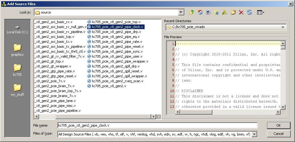
33 Compile Example Design Add kc705_pcie_x8_gen2_pipe_clock.v

34 Compile Example Design Click Add Directories

35 Compile Example Design Add the example_design directory from the PCIe source files
36 Compile Example Design Click Finish
37 Compile Example Design Click Add Sources again

38 Compile Example Design Select Add or Create Constraints
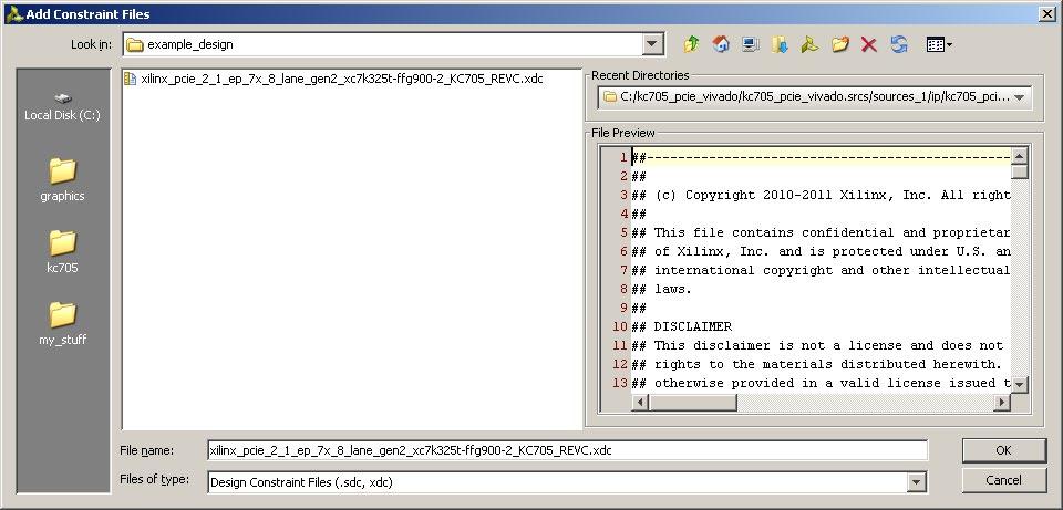
39 Compile Example Design Add xilinx_pcie_2_1_ep_7x_8_lane_gen2_xc7k325t-ffg900-2_kc705_revc.xdc

40 Compile Example Design Click Finish

41 Compile Example Design Click on Generate Bitstream

42 Compile Example Design The completed design appears in GUI

43 Hardware Setup Set S13 to (1 = on, Position 1 Position 5) This enables Master BPI configuration from Slot #1 Flash A25, A24 = 00 FPGA mode pins M[2:0] = 010

44 KC705 Setup Connect a USB Type-A to Micro-B cable to the USB JTAG (Digilent) connector on the KC705 board Connect this cable to your PC Power on the KC705 board
45 Generate x8 Gen 2 PCIe MCS File
46 Generate PCIe MCS File Click on Launch impact

47 Generate PCIe MCS File Under impact Flows, double click on Create a PROM File
48 Generate PCIe MCS File To generate a PROM file for the BPI Flash, select: BPI Configure Single FPGA

49 Generate PCIe MCS File Select Virtex7 Add 128M Storage Device


50 Generate PCIe MCS File Click on Output File Location, create a ready_for_download directory, set the file name, set Data Width to 16, and click OK

51 Generate PCIe MCS File Add xilinx_pcie_2_1_ep_7x.bit from the <design path>\kc705_pcie_vivado.runs\impl_1 directory

52 Generate PCIe MCS File Click OK on this dialog
53 Generate PCIe MCS File From the impact menu, select Operations Generate File
54 Program BPI Flash with PCIe Design After generation completes, click on the Boundary Scan tab

55 Program BPI Flash with PCIe Design Right click on the SPI/BPI? and select Add SPI/BPI Flash Add <design path>\ready_for_download\kc705_pcie_x8_gen2.mcs

56 Program BPI Flash with PCIe Design Make the following settings Select 28F00AP30 Set the RS Pins to 25:24

57 Note: Programming takes about 2 minutes Program BPI Flash with PCIe Design Right click on the Flash and select Program Use default settings to Erase and Verify device

58 Program BPI Flash with PCIe Design Erase Before Programming must be selected
 Use the included PC Power adapter; turn on Power")
59 Hardware Setup Insert the KC705 Board into a PCIe slot (x16 shown) Use the included PC Power adapter; turn on Power Switch


60 Hardware Setup Do not use the PCIe connector from the PC power supply
61 Running the PCIe x8 Gen 2 Design Power on the PC Start PciTree
62 Running the PCIe x8 Gen 2 Design Set Number of Configuration Registers to 64 Click on Refresh dump
63 Running the PCIe x8 Gen 2 Design Locate the Xilinx Device Vendor ID is 0x10EE The x8 Gen 2 configuration will have a Device ID of 0x7028
64 Running the PCIe x8 Gen 2 Design Navigate the linked list in configuration space to locate the PCIe Capabilities Structure See UG477 for details With the Xilinx device selected, select Register 0x40 Register 0x40 points to the next structure 0x48 is the address of the next structure
65 Running the PCIe x8 Gen 2 Design Select Register 0x48 Register 0x48 points to the next structure 0x60 is the address of the next structure

66 Running the PCIe x8 Gen 2 Design Register 0x60 0x60 is a type 0x10, indicating PCIe Capabilities Structure Last Structure
67 Running the PCIe x8 Gen 2 Design 1 Register 0x6C Link Capabilities Register Indicates the maximum number of lanes and speed (Gen 1, Gen 2) for device The value 0x82 shows this is an x8 Gen 2 device (1) Link Status Register 0x70 Shows the current link status This design, in a Gen 2 chassis, trained to x8 Gen 2 (2) 2

68 Running the PCIe x8 Gen 2 Design Double-click on BAR 0 BAR 0 Address is machine dependent Click Yes on the Dialog box seen below
69 Running the PCIe x8 Gen 2 Design Select auto read memory

70 Running the PCIe x8 Gen 2 Design Click on the first memory location Type <Shift-End> to select 1024 Bytes
71 Running the PCIe x8 Gen 2 Design Write Memory Select count Click Write Memory Click refr view View results counting up to FF

72 Running the PCIe x8 Gen 2 Design Restore Memory Deselect count Click Write Memory Click refr view Memory is reset to zeros Turn off PCIe chassis and remove KC705 board
73 References
74 References PCIe Base Specification PCI SIG Web Site Kintex-7 PCIe PCIe Product Overview 7_SERIES_PCI_Express_Block.htm 7 Series FPGAs Integrated Block for PCI Express User Guide UG477 pcie_7x/v1_4/ug477_7series_intblock_pcie.pdf 7 Series FPGAs Integrated Block for PCI Express Data Sheet DS821 pcie_7x/v1_4/ds821_7series_pcie.pdf IP Release Notes Guide
75 Documentation
76 Documentation Kintex-7 Kintex-7 FPGA Family KC705 Documentation Kintex-7 FPGA KC705 Evaluation Kit KC705 Getting Started Guide ug883_k7_kc705_eval_kit.pdf KC705 User Guide ug810_kc705_eval_bd.pdf KC705 Reference Design User Guide ug845_ref_design.pdf
ML605 PCIe x8 Gen1 Design Creation
 ML605 PCIe x8 Gen1 Design Creation October 2010 Copyright 2010 Xilinx XTP044 Revision History Date Version Description 10/05/10 12.3 Recompiled under 12.3. AR35422 fixed; included in ISE tools. 07/23/10
ML605 PCIe x8 Gen1 Design Creation
 ML605 PCIe x8 Gen1 Design Creation March 2010 Copyright 2010 Xilinx XTP044 Note: This presentation applies to the ML605 Overview Virtex-6 PCIe x8 Gen1 Capability Xilinx ML605 Board Software Requirements
KC705 Ethernet Design Creation October 2012
 KC705 Ethernet Design Creation October 2012 XTP147 Revision History Date Version Description 10/23/12 4.0 Regenerated for 14.3. 07/25/12 3.0 Regenerated for 14.2. Added AR50886. 05/08/12 2.0 Regenerated
ZC706 GTX IBERT Design Creation June 2013
 ZC706 GTX IBERT Design Creation June 2013 XTP243 Revision History Date Version Description 06/19/13 4.0 Recompiled for Vivado 2013.2. 04/16/13 3.1 Added AR54225. 04/03/13 3.0 Recompiled for 14.5. 01/18/13
AC701 Ethernet Design Creation June 2014
 AC701 Ethernet Design Creation June 2014 XTP223 Revision History Date Version Description 06/09/14 8.0 Regenerated for 2014.2. 04/16/14 6.0 Regenerated for 2014.1. 12/18/13 5.0 Regenerated for 2013.4.
AC701 Ethernet Design Creation October 2014
 AC701 Ethernet Design Creation October 2014 XTP223 Revision History Date Version Description 10/08/14 9.0 Regenerated for 2014.3. 06/09/14 8.0 Regenerated for 2014.2. 04/16/14 6.0 Regenerated for 2014.1.
ML605 Restoring Flash Contents
 ML605 Restoring Flash Contents March 2011 Copyright 2011 Xilinx XTP055 Revision History Date Version Description 03/01/11 13.1 Regenerated contents for 13.1. 12/21/10 12.4 Regenerated contents for 12.4.
KC705 GTX IBERT Design Creation October 2012
 KC705 GTX IBERT Design Creation October 2012 XTP103 Revision History Date Version Description 10/23/12 4.0 Regenerated for 14.3. 07/25/12 3.0 Regenerated for 14.2. Added AR50886. 05/30/12 2.1 Minor updates.
ZC706 GTX IBERT Design Creation November 2014
 ZC706 GTX IBERT Design Creation November 2014 XTP243 Revision History Date Version Description 11/24/14 10.0 Regenerated for 2014.4. 10/08/14 9.0 Regenerated for 2014.3. 06/09/14 8.0 Regenerated for 2014.2.
KC705 Si5324 Design October 2012
 KC705 Si5324 Design October 2012 XTP188 Revision History Date Version Description 10/23/12 4.0 Recompiled for 14.3. 07/25/12 3.0 Recompiled for 14.2. Added AR50886. 05/08/12 2.0 Recompiled for 14.1. 02/14/12
KC705 Si570 Programming
 KC705 Si570 Programming March 2012 Copyright 2012 Xilinx XTP186 Revision History Date Version Description 03/02/12 13.4 Initial version. Copyright 2012 Xilinx, Inc. All Rights Reserved. XILINX, the Xilinx
VCU110 GT IBERT Design Creation
 VCU110 GT IBERT Design Creation June 2016 XTP374 Revision History Date Version Description 06/08/16 4.0 Updated for 2016.2. 04/13/16 3.0 Updated for 2016.1. Updated for Production Kit. 02/03/16 2.1 Updated
SP605 MultiBoot Design
 SP605 MultiBoot Design October 2010 Copyright 2010 Xilinx XTP059 Revision History Date Version Description 10/05/10 12.3 Recompiled under 12.3. 07/23/10 12.2 Recompiled under 12.2. Copyright 2010 Xilinx,
AC701 Built-In Self Test Flash Application April 2015
 AC701 Built-In Self Test Flash Application April 2015 XTP194 Revision History Date Version Description 04/30/14 11.0 Recompiled for 2015.1. Removed Ethernet as per CR861391. 11/24/14 10.0 Recompiled for
VCU108 Built In Test July 2015
 VCU108 Built In Test July 2015 XTP361 Revision History Date Version Description 07/15/15 2.0 Updated for 2015.2. 06/30/15 1.0 Initial version for 2015.1. Copyright 2015 Xilinx, Inc. All Rights Reserved.
ML631 U1 DDR3 MIG Design Creation
 ML631 U1 DDR3 MIG Design Creation October 2011 Copyright 2011 Xilinx XTP112 Revision History Date Version Description 10/26/11 13.3 Updated for 13.3. 08/30/11 13.2 Initial version. Copyright 2011 Xilinx,
ML631 U2 DDR3 MIG Design Creation
 ML631 U2 DDR3 MIG Design Creation March 2012 Copyright 2012 Xilinx XTP129 Revision History Date Version Description 03/16/12 13.4 Updated for 13.4 10/26/11 13.3 Updated for 13.3. 08/30/11 13.2 Initial
ML605 GTX IBERT Design Creation
 ML605 GTX IBERT Design Creation December 2010 Copyright 2010 Xilinx XTP046 Revision History Date Version Description 12/21/10 12.4 Recompiled under 12.4. 10/05/10 12.3 Recompiled under 12.3. AR36576 fixed.
SP605 GTP IBERT Design Creation
 SP605 GTP IBERT Design Creation October 2010 Copyright 2010 Xilinx XTP066 Revision History Date Version Description 10/05/10 12.3 Recompiled under 12.3. ARs Present in Spartan-6 IBERT Design: AR36775 Delay
ZC702 Si570 Programming June 2012
 June 2012 XTP181 Revision History Date Version Description 05/25/12 1.0 Initial version for 14.1. Copyright 2012 Xilinx, Inc. All Rights Reserved. XILINX, the Xilinx logo, the Brand Window and other designated
VCU110 Software Install and Board Setup October 2015
 VCU110 Software Install and Board Setup October 2015 XTP380 Revision History Date Version Description 11/20/15 1.2 Modified to match VCU110 Kit hardware. 10/22/15 1.1 Added ExaMax and Interlaken setup.
SP605 Standalone Applications
 SP605 Standalone Applications July 2011 Copyright 2011 Xilinx XTP064 Revision History Date Version Description 07/06/11 13.2 Up-rev 13.1 GPIO_HDR Design to 13.2. 03/01/11 13.1 Up-Rev 12.4 GPIO_HDR Design
ZC706 Built-In Self Test Flash Application April 2015
 ZC706 Built-In Self Test Flash Application April 2015 XTP242 Revision History Date Version Description 04/30/15 11.0 Recompiled for 2015.1. 11/24/14 10.0 Recompiled for 2014.4. 10/08/14 9.0 Recompiled
ML605 FMC Si570 Programming June 2012
 ML605 FMC Si570 Programming June 2012 XTP076 Revision History Date Version Description 06/15/12 1.0 Initial version for 13.4. Copyright 2012 Xilinx, Inc. All Rights Reserved. XILINX, the Xilinx logo, the
ML605 Built-In Self Test Flash Application
 ML605 Built-In Self Test Flash Application July 2011 Copyright 2011 Xilinx XTP056 Revision History Date Version Description 07/06/11 13.2 Up-rev 13.1 BIST Design to 13.2. 03/01/11 13.1 Up-rev 12.4 BIST
ML605 Built-In Self Test Flash Application
 ML605 Built-In Self Test Flash Application October 2010 Copyright 2010 Xilinx XTP056 Revision History Date Version Description 10/05/10 12.3 Up-rev 12.2 BIST Design to 12.3. Added AR38127 Added AR38209
SP605 Built-In Self Test Flash Application
 SP605 Built-In Self Test Flash Application March 2011 Copyright 2011 Xilinx XTP062 Revision History Date Version Description 03/01/11 13.1 Up-rev 12.4 BIST Design to 13.1. 12/21/10 12.4 Up-rev 12.3 BIST
PlanAhead Software Tutorial
 PlanAhead Software Tutorial RTL Design and IP Generation The information disclosed to you hereunder (the Information ) is provided AS-IS with no warranty of any kind, express or implied. Xilinx does not
Vivado Design Suite Tutorial. Designing IP Subsystems Using IP Integrator
 Vivado Design Suite Tutorial Designing IP Subsystems Using IP Integrator Notice of Disclaimer The information disclosed to you hereunder (the "Materials") is provided solely for the selection and use of
Vivado Design Suite Tutorial. Designing IP Subsystems Using IP Integrator
 Vivado Design Suite Tutorial Designing IP Subsystems Using IP Integrator Notice of Disclaimer The information disclosed to you hereunder (the "Materials") is provided solely for the selection and use of
Quick Front-to-Back Overview Tutorial
 Quick Front-to-Back Overview Tutorial PlanAhead Design Tool This tutorial document was last validated using the following software version: ISE Design Suite 14.5 If using a later software version, there
Virtual Input/Output v3.0
 Virtual Input/Output v3.0 LogiCORE IP Product Guide Vivado Design Suite Table of Contents IP Facts Chapter 1: Overview Feature Summary..................................................................
SP605 MultiBoot Design
 SP605 MultiBoot Design December 2009 Copyright 2009 Xilinx XTP059 Note: This presentation applies to the SP605 Overview Spartan-6 MultiBoot Capability Xilinx SP605 Board Software Requirements SP605 Setup
SP601 MultiBoot Design
 SP601 MultiBoot Design December 2009 Copyright 2009 Xilinx XTP038 Note: This presentation applies to the SP601 Overview Spartan-6 MultiBoot Capability Xilinx SP601 Board Software Requirements SP601 Setup
RTL Design and IP Generation Tutorial. PlanAhead Design Tool
 RTL Design and IP Generation Tutorial PlanAhead Design Tool Notice of Disclaimer The information disclosed to you hereunder (the "Materials") is provided solely for the selection and use of Xilinx products.
ISim Hardware Co-Simulation Tutorial: Accelerating Floating Point FFT Simulation
 ISim Hardware Co-Simulation Tutorial: Accelerating Floating Point FFT Simulation UG817 (v 14.3) October 16, 2012 This tutorial document was last validated using the following software version: ISE Design
Vivado Design Suite Tutorial. I/O and Clock Planning
 Vivado Design Suite Tutorial I/O and Clock Planning Notice of Disclaimer The information disclosed to you hereunder (the "Materials") is provided solely for the selection and use of Xilinx products. To
Vivado Design Suite Tutorial
 Vivado Design Suite Tutorial Designing IP Subsystems Using IP Integrator Revision History Date Version Revision 11/19/2014 2014.4 Validated with this release. 10/01/2014 2014.3 Validated with this release.
ISim Hardware Co-Simulation Tutorial: Accelerating Floating Point Fast Fourier Transform Simulation
 ISim Hardware Co-Simulation Tutorial: Accelerating Floating Point Fast Fourier Transform Simulation UG817 (v 13.2) July 28, 2011 Xilinx is disclosing this user guide, manual, release note, and/or specification
Supported Device Family (1) Supported User Interfaces. Simulation Models Supported S/W Drivers. Simulation. Notes:
 Supported User Interfaces. Simulation Models Supported S/W Drivers. Simulation. Notes:") LogiCORE IP CPRI v8.5 Introduction The LogiCORE IP Common Public Radio Interface (CPRI ) core is a high-performance, low-cost flexible solution for implementation of the CPRI interface. The core can be
LogiCORE IP CPRI v8.5 Introduction The LogiCORE IP Common Public Radio Interface (CPRI ) core is a high-performance, low-cost flexible solution for implementation of the CPRI interface. The core can be
Vivado Design Suite User Guide
 Vivado Design Suite User Guide Design Flows Overview Notice of Disclaimer The information disclosed to you hereunder (the Materials ) is provided solely for the selection and use of Xilinx products. To
Vivado Design Suite User Guide. Designing IP Subsystems Using IP Integrator
 Vivado Design Suite User Guide Designing IP Subsystems Using IP Integrator Notice of Disclaimer The information disclosed to you hereunder (the "Materials") is provided solely for the selection and use
Vivado Design Suite Tutorial. Designing IP Subsystems Using IP Integrator
 Vivado Design Suite Tutorial Designing IP Subsystems Using IP Integrator Notice of Disclaimer The information disclosed to you hereunder (the Materials ) is provided solely for the selection and use of
Vivado Design Suite Tutorial. I/O and Clock Planning
 Vivado Design Suite Tutorial I/O and Clock Planning Notice of Disclaimer The information disclosed to you hereunder (the "Materials") is provided solely for the selection and use of Xilinx products. To
Vivado Design Suite User Guide
 Vivado Design Suite User Guide Design Flows Overview Notice of Disclaimer The information disclosed to you hereunder (the Materials ) is provided solely for the selection and use of Xilinx products. To
Vivado Design Suite Tutorial. Using Constraints
 Vivado Design Suite Tutorial Using Constraints Notice of Disclaimer The information disclosed to you hereunder (the "Materials") is provided solely for the selection and use of Xilinx products. To the
MultiBoot and Fallback Using ICAP in UltraScale+ FPGAs
 XAPP1296 (v1.0) June 23, 2017 Application Note: UltraScale+ FPGAs MultiBoot and Fallback Using ICAP in UltraScale+ FPGAs Author: Guruprasad Kempahonnaiah Summary This application note describes a key feature
ISim Hardware Co-Simulation Tutorial: Accelerating Floating Point FFT Simulation
 ISim Hardware Co-Simulation Tutorial: Accelerating Floating Point FFT Simulation UG817 (v13.3) November 11, 2011 Xilinx is disclosing this user guide, manual, release note, and/or specification (the Documentation
ISim Hardware Co-Simulation Tutorial: Processing Live Ethernet Traffic through Virtex-5 Embedded Ethernet MAC
 ISim Hardware Co-Simulation Tutorial: Processing Live Ethernet Traffic through Virtex-5 Embedded Ethernet MAC UG819 (v 13.1) March 18, 2011 Xilinx is disclosing this user guide, manual, release note, and/or
Using Xilinx ChipScope Pro ILA Core with Project Navigator to Debug FPGA Applications. UG750 (v12.3) November 5, 2010
 November 5, 2010") Using Xilinx ChipScope Pro ILA Core with Project Navigator to Debug FPGA Applications UG750 (v12.3) November 5, 2010 Xilinx is disclosing this user guide, manual, release note, and/or specification (the
Using Xilinx ChipScope Pro ILA Core with Project Navigator to Debug FPGA Applications UG750 (v12.3) November 5, 2010 Xilinx is disclosing this user guide, manual, release note, and/or specification (the
Quick Start Guide ZedboardOLED Display Controller IP v1.0
 Quick Start Guide Introduction This document provides instructions to quickly add, connect and use the ZedboardOLED v1.0 IP core. A test application running on an ARM processor system is used to communicate
7 Series FPGAs Memory Interface Solutions (v1.9)
") 7 Series FPGAs Memory Interface Solutions (v1.9) DS176 March 20, 2013 Introduction The Xilinx 7 series FPGAs memory interface solutions cores provide high-performance connections to DDR3 and DDR2 SDRAMs,
7 Series FPGAs Memory Interface Solutions (v1.9) DS176 March 20, 2013 Introduction The Xilinx 7 series FPGAs memory interface solutions cores provide high-performance connections to DDR3 and DDR2 SDRAMs,
Hierarchical Design Using Synopsys and Xilinx FPGAs
 White Paper: FPGA Design Tools WP386 (v1.0) February 15, 2011 Hierarchical Design Using Synopsys and Xilinx FPGAs By: Kate Kelley Xilinx FPGAs offer up to two million logic cells currently, and they continue
I/O Pin Planning Tutorial. PlanAhead Design Tool
 I/O Pin Planning Tutorial PlanAhead Design Tool Notice of Disclaimer The information disclosed to you hereunder (the "Materials") is provided solely for the selection and use of Xilinx products. To the
Kintex-7 FPGA Base Targeted Reference Design
 Kintex-7 FPGA Base Targeted Reference Design User Guide Notice of Disclaimer The information disclosed to you hereunder (the Materials ) is provided solely for the selection and use of Xilinx products.
ISE Tutorial. Using Xilinx ChipScope Pro ILA Core with Project Navigator to Debug FPGA Applications. UG750 (v14.4) December 18, 2012
 December 18, 2012") ISE Tutorial Using Xilinx ChipScope Pro ILA Core with Project Navigator to Debug FPGA Applications UG750 (v14.4) December 18, 2012 Xilinx is disclosing this user guide, manual, release note, and/or specification
ISE Tutorial Using Xilinx ChipScope Pro ILA Core with Project Navigator to Debug FPGA Applications UG750 (v14.4) December 18, 2012 Xilinx is disclosing this user guide, manual, release note, and/or specification
ISE Tutorial: Using Xilinx ChipScope Pro ILA Core with Project Navigator to Debug FPGA Applications
 ISE Tutorial: Using Xilinx ChipScope Pro ILA Core with Project Navigator to Debug FPGA Applications This tutorial document was last validated using the following software version: ISE Design Suite 14.5
PetaLinux SDK User Guide. Eclipse Plugin Guide
 PetaLinux SDK User Guide Notice of Disclaimer The information disclosed to you hereunder (the "Materials") is provided solely for the selection and use of Xilinx products. To the maximum extent permitted
Vivado Design Suite Tutorial:
 Vivado Design Suite Tutorial: Programming and Debugging Notice of Disclaimer The information disclosed to you hereunder (the Materials ) is provided solely for the selection and use of Xilinx products.
Intel Stratix 10 H-Tile PCIe Link Hardware Validation
 Intel Stratix 10 H-Tile PCIe Link Hardware Validation Subscribe Send Feedback Latest document on the web: PDF HTML Contents Contents 1. Intel Stratix 10 H-Tile PCIe* Link Hardware Validation... 3 1.1.
I/O Planning Tutorial. PlanAhead Design Tool
 I/O Planning Tutorial PlanAhead Design Tool This tutorial document was last validated using the following software version: ISE Design Suite 15 If using a later software version, there may be minor differences
Accelerating System Designs Requiring High-Bandwidth Connectivity with Targeted Reference Designs
 White Paper: Spartan-6 and Virtex-6 FPGAs WP359 (v1.0) December 8, 2009 Accelerating System Designs Requiring High-Bandwidth Connectivity with Targeted Reference Designs By: Navneet Rao FPGAs that provide
Vivado Design Suite User Guide
 Vivado Design Suite User Guide System-Level Design Entry Notice of Disclaimer The information disclosed to you hereunder (the Materials ) is provided solely for the selection and use of Xilinx products.
EXOSTIV Dashboard Hands-on - MICA board
 EXOSTIV Dashboard Hands-on - MICA board Rev. 1.0.5 - October 18, 2017 http://www.exostivlabs.com 1 Table of Contents EXOSTIV Dashboard Hands-on...3 Introduction...3 EXOSTIV for Xilinx FPGA Overview...3
Virtex-6 FPGA Connectivity Kit
 Virtex-6 FPGA Connectivity Kit Getting Started Guide XPN 0402826-03 Notice of Disclaimer The information disclosed to you hereunder (the Materials ) is provided solely for the selection and use of Xilinx
Data Side OCM Bus v1.0 (v2.00b)
") 0 Data Side OCM Bus v1.0 (v2.00b) DS480 January 23, 2007 0 0 Introduction The DSOCM_V10 core is a data-side On-Chip Memory (OCM) bus interconnect core. The core connects the PowerPC 405 data-side OCM interface
0 Data Side OCM Bus v1.0 (v2.00b) DS480 January 23, 2007 0 0 Introduction The DSOCM_V10 core is a data-side On-Chip Memory (OCM) bus interconnect core. The core connects the PowerPC 405 data-side OCM interface
Interlaken IP Core (2nd Generation) Design Example User Guide
 Design Example User Guide") Interlaken IP Core (2nd Generation) Design Example User Guide UG-20051 2017.09.19 Subscribe Send Feedback Contents Contents 1 Quick Start Guide... 3 1.1 Directory Structure... 4 1.2 Design Components...
Interlaken IP Core (2nd Generation) Design Example User Guide UG-20051 2017.09.19 Subscribe Send Feedback Contents Contents 1 Quick Start Guide... 3 1.1 Directory Structure... 4 1.2 Design Components...
Virtex-6 FPGA Connectivity Kit
 Virtex-6 FPGA Connectivity Kit Getting Started Guide XPN 0402826-01 Xilinx is disclosing this user guide, manual, release note, and/or specification (the Documentation ) to you solely for use in the development
Designing with the Xilinx 7 Series PCIe Embedded Block. Tweet this event: #avtxfest
 Designing with the Xilinx 7 Series PCIe Embedded Block Follow @avnetxfest Tweet this event: #avtxfest www.facebook.com/xfest2012 Why Would This Presentation Matter to You? 2 If you are designing a PCIe
Utility Bus Split (v1.00a)
") DS484 December 2, 2009 Introduction The Utility Bus Split core splits a bus into smaller buses using the Xilinx Platform Studio (XPS). The core splits one input bus into two output buses which serve as
DS484 December 2, 2009 Introduction The Utility Bus Split core splits a bus into smaller buses using the Xilinx Platform Studio (XPS). The core splits one input bus into two output buses which serve as
I/O Pin Planning Tutorial. PlanAhead Design Tool
 I/O Pin Planning Tutorial PlanAhead Design Tool Xilinx is disclosing this user guide, manual, release note, and/or specification (the Documentation ) to you solely for use in the development of designs
PlanAhead Software Tutorial
 PlanAhead Software Tutorial Team Design NOTICE OF DISCLAIMER: The information disclosed to you hereunder (the Information ) is provided AS-IS with no warranty of any kind, express or implied. Xilinx does
Vivado Design Suite Tutorial: Programming and Debugging
 Vivado Design Suite Tutorial: Programming and Debugging Notice of Disclaimer The information disclosed to you hereunder (the "Materials") is provided solely for the selection and use of Xilinx products.
Lab 1 - Zynq RTL Design Flow
 NTU GIEE, MULTIMEDIA SYSTEM-ON-CHIP DESIGN Lab 1 - Zynq RTL Design Flow Pin-Hung Kuo May 11, 2018 1 INTRODUCTION In this lab, we are going to build a simple Zynq system on ZedBoard. This system works as
Vivado Design Suite User Guide
 Vivado Design Suite User Guide Using the Vivado IDE Notice of Disclaimer The information disclosed to you hereunder (the Materials ) is provided solely for the selection and use of Xilinx products. To
Vivado Design Suite Tutorial: Implementation
 Vivado Design Suite Tutorial: Implementation Notice of Disclaimer The information disclosed to you hereunder (the Materials ) is provided solely for the selection and use of Xilinx products. To the maximum
Author: Kiran K Gakhal
 Application Note: 7 Series FPGAs XAPP1246 (v1.1) February 28, 2017 MultiBoot with 7 Series FPGAs and BPI Author: Kiran K Gakhal Summary Note: Spartan -7 devices do not support BPI. This application note
PlanAhead Software Tutorial
 PlanAhead Software Tutorial I/O Pin Planning The information disclosed to you hereunder (the Information ) is provided AS-IS with no warranty of any kind, express or implied. Xilinx does not assume any
StickIt! MPU-9150 Manual. How to install and use your new StickIt! MPU-9150 Module
 StickIt! MPU-9150 Manual How to install and use your new StickIt! MPU-9150 Module XESS is disclosing this Document and Intellectual Property (hereinafter the Design ) to you for use in the development
Vivado Design Suite Tutorial. Design Flows Overview
 Vivado Design Suite Tutorial Design Flows Overview Notice of Disclaimer The information disclosed to you hereunder (the "Materials") is provided solely for the selection and use of Xilinx products. To
Vivado Design Suite Tutorial. Designing with IP
 Vivado Design Suite Tutorial Designing with IP Notice of Disclaimer The information disclosed to you hereunder (the "Materials") is provided solely for the selection and use of Xilinx products. To the
Vivado Design Suite Tutorial:
 Vivado Design Suite Tutorial: Programming and Debugging Notice of Disclaimer The information disclosed to you hereunder (the Materials ) is provided solely for the selection and use of Xilinx products.
Getting Started Guide with AXM-A30
 Series PMC-VFX70 Virtex-5 Based FPGA PMC Module Getting Started Guide with AXM-A30 ACROMAG INCORPORATED Tel: (248) 295-0310 30765 South Wixom Road Fax: (248) 624-9234 P.O. BOX 437 Wixom, MI 48393-7037
Hardware In The Loop (HIL) Simulation for the Zynq-7000 All Programmable SoC Author: Umang Parekh
 Simulation for the Zynq-7000 All Programmable SoC Author: Umang Parekh") Application Note: Zynq-7000 AP SoC XAPP744 (v1.0.2) November 2, 2012 Hardware In The Loop (HIL) Simulation for the Zynq-7000 All Programmable SoC Author: Umang Parekh Summary The Zynq -7000 All Programmable
Application Note: Zynq-7000 AP SoC XAPP744 (v1.0.2) November 2, 2012 Hardware In The Loop (HIL) Simulation for the Zynq-7000 All Programmable SoC Author: Umang Parekh Summary The Zynq -7000 All Programmable
Utility Reduced Logic (v1.00a)
") DS482 December 2, 2009 Introduction The Utility Reduced Logic core applies a logic reduction function over an input vector to generate a single bit result. The core is intended as glue logic between peripherals.
DS482 December 2, 2009 Introduction The Utility Reduced Logic core applies a logic reduction function over an input vector to generate a single bit result. The core is intended as glue logic between peripherals.
ChipScope Pro Software and Cores User Guide
 ChipScope Pro Software and Cores User Guide (ChipScope Pro Software v7.1i) R Xilinx is disclosing this Document and Intellectual Property (hereinafter the Design ) to you for use in the development of
SP605 GTP IBERT Design Creation
 SP605 GTP IBERT Design Creation January 2010 Copyright 2009, 2010 Xilinx XTP066 Note: This Presentation applies to the SP605 SP605 IBERT Overview Xilinx SP605 Board Software Requirements Setup for the
LogiCORE IP 3GPP LTE Turbo Encoder v1.0 Bit-Accurate C Model. 3GPP LTE Turbo. [optional] UG490 (v1.0) April 25, 2008 [optional]
![LogiCORE IP 3GPP LTE Turbo Encoder v1.0 Bit-Accurate C Model. 3GPP LTE Turbo. [optional] UG490 (v1.0) April 25, 2008 [optional]](/thumbs/85/91367790.jpg "LogiCORE IP 3GPP LTE Turbo Encoder v1.0 Bit-Accurate C Model. 3GPP LTE Turbo. [optional] UG490 (v1.0) April 25, 2008 [optional]") LogiCORE IP 3GPP LTE Turbo Encoder v1.0 Bit-Accurate C Model LogiCORE IP 3GPP LTE Turbo Encoder v1.0 [Guide User Guide Subtitle] [optional] [optional] R R Xilinx is disclosing this user guide, manual,
LogiCORE IP 3GPP LTE Turbo Encoder v1.0 Bit-Accurate C Model LogiCORE IP 3GPP LTE Turbo Encoder v1.0 [Guide User Guide Subtitle] [optional] [optional] R R Xilinx is disclosing this user guide, manual,
SPI x4 Configuration Demo on SP601 Board. Boris Qin
 SPI x4 Configuration Demo on SP601 Board Boris Qin Agenda Why do we use SPI x4? How to use the Demo design? How to create the SPI x4 design? Measurements compared to the calculations Page 2 Why do we use
ZedBoard: Zynq-7000 AP SoC Concepts, Tools, and Techniques
 ZedBoard: Zynq-7000 AP SoC Concepts, Tools, and Techniques A Hands-On Guide to Effective Embedded System Design ZedBoard (Vivado 2014.2) Notice of Disclaimer The information disclosed to you hereunder
Zynq-7000 Bus Functional Model
 DS897 May 24, 2013 Introduction The Zynq -7000 Bus Functional Model (BFM) supports the functional simulation of Zynq-7000 based applications. It is targeted to enable the functional verification of Programmable
Creating the AVS6LX9MBHP211 MicroBlaze Hardware Platform for the Spartan-6 LX9 MicroBoard Version
 Creating the AVS6LX9MBHP211 MicroBlaze Hardware Platform for the Spartan-6 LX9 MicroBoard Version 13.2.01 Revision History Version Description Date 12.4.01 Initial release for EDK 12.4 09 Mar 2011 12.4.02
Zynq-7000 Platform Software Development Using the ARM DS-5 Toolchain Author: Simon George and Prushothaman Palanichamy
 Application Note: Zynq-7000 All Programmable SoC XAPP1185 (v1.0) November 18, 2013 Zynq-7000 Platform Software Development Using the ARM DS-5 Toolchain Author: Simon George and Prushothaman Palanichamy
High Bandwidth Memory (HBM2) Interface Intel FPGA IP Design Example User Guide
 Interface Intel FPGA IP Design Example User Guide") High Bandwidth Memory (HBM2) Interface Intel FPGA IP Design Example Updated for Intel Quartus Prime Design Suite: 18.1.1 Subscribe Latest document on the web: PDF HTML Contents Contents 1. High Bandwidth
High Bandwidth Memory (HBM2) Interface Intel FPGA IP Design Example Updated for Intel Quartus Prime Design Suite: 18.1.1 Subscribe Latest document on the web: PDF HTML Contents Contents 1. High Bandwidth
Understanding Performance of PCI Express Systems
 White Paper: Virtex-4 and Virtex-5 FPGAs R WP350 (v1.1) September 4, 2008 Understanding Performance of PCI Express Systems By: Alex Goldhammer and John Ayer Jr. PCI Express technology, which is a serialized
ISE Simulator (ISim) In-Depth Tutorial. UG682 (v 13.1) March 1, 2011
 In-Depth Tutorial. UG682 (v 13.1) March 1, 2011") ISE Simulator (ISim) In-Depth Tutorial Xilinx is disclosing this user guide, manual, release note, and/or specification (the "Documentation") to you solely for use in the development of designs to operate
ISE Simulator (ISim) In-Depth Tutorial Xilinx is disclosing this user guide, manual, release note, and/or specification (the "Documentation") to you solely for use in the development of designs to operate
Configuring the Xilinx Spartan-6 LX9 MicroBoard
 Configuring the Xilinx Spartan-6 LX9 MicroBoard Version 1.3 Table of Contents Table of Contents... 2 Table of Figures... 3 Revision History... 4 Overview... 5 Configuration and Programming via the on-board
AXI4 Interconnect Paves the Way to Plug-and-Play IP
 White Paper: Virtex-6 and Spartan-6 FPGAs WP379 (v1.0) October 5, 2010 4 Interconnect Paves the Way to Plug-and-Play IP By: Navanee Sundaramoorthy, Navneet Rao, and Tom Hill In the past decade, the size
PetaLinux SDK User Guide. Firmware Upgrade Guide
 PetaLinux SDK User Guide Notice of Disclaimer The information disclosed to you hereunder (the "Materials") is provided solely for the selection and use of Xilinx products. To the maximum extent permitted
Virtex-4 PowerPC Example Design. UG434 (v1.2) January 17, 2008
 January 17, 2008") Virtex-4 PowerPC Example Design R R 2007-2008 Xilinx, Inc. All Rights Reserved. XILINX, the Xilinx logo, and other designated brands included herein are trademarks of Xilinx, Inc. All other trademarks
Virtex-4 PowerPC Example Design R R 2007-2008 Xilinx, Inc. All Rights Reserved. XILINX, the Xilinx logo, and other designated brands included herein are trademarks of Xilinx, Inc. All other trademarks