Tutorial on FPGA Design Flow based on Aldec Active HDL. ver 1.6
|
|
|
- Gerard Hunter
- 6 years ago
- Views:
Transcription
1 Tutorial on FPGA Design Flow based on Aldec Active HDL ver 1.6 Fall
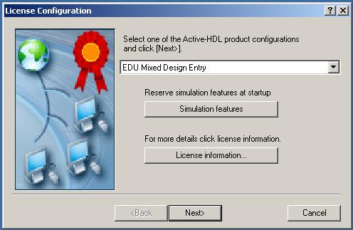
2 Prepared by Ekawat (Ice) Homsirikamol, Marcin Rogawski, Jeremy Kelly, Kishore Kumar Surapathi, Ambarish Vyas, Umar Sharif and Dr. Kris Gaj Note: This tutorial assumes that you have basic knowledge on how to use Aldec Active HDL and its functional simulation. The example codes used in this tutorial can be obtained from: Preparing the Input: Go to the link given above and dowload following files. 1. Synthesizable VHDL Codes: a. clock_divider.vhd b. counter.vhd c. SSegCtrl.vhd d. lab3_demo_package.vhd e. lab3_demo.vhd 2. Testbench: lab3_demo_tb.vhd 3. User Constraints File: lab3_demo_ucf.ucf 4. Bitstream: lab3_demo_bitstream.bit (used only if you work with the FPGA board). Current Version of Tools: This tutorial has been tested using the following tools CAD Tools ActiveHDL Versions: 7.2, 8.2, 8.3 Synthesis Tools o Xilinx ISE Webpack XST Versions: 9.1, 10.1, 12.2, 12.4, 13.2 o Synplify Premier DP Version: D Implementation Tool o Xilinx ISE/WebPack Versions: 9.1, 10.1, 12.2, 12.4, 13.2 FPGA Board Digilent Basys2 The combinations of tools supported as of Fall 2011 are as follows: At home: Aldec Active-HDL Student Edition ver. 7.2 Xilinx ISE/Webpack 9.1 SP3 At GMU: Aldec Active-HDL ver. 8.3 SP1 Xilinx ISE/Webpack 13.2 Synplify Premier DP D
3 Table of Contents 1 Project Settings 4 2 Synthesis 2.1 Synthesis using Xilinx XST Synthesis Options Synthesis Report 2.2 Synthesis using Synplify Premier DP Synthesis Options Synthesis Report 2.3 Post-Synthesis Simulation 33 3 Implementation 3.1 Implementation Options Implementation Reports Timing Simulation 44 4 Uploading Bitstream to FPGA Board 46 3

4 1. Project Settings 4
5 5
6 6

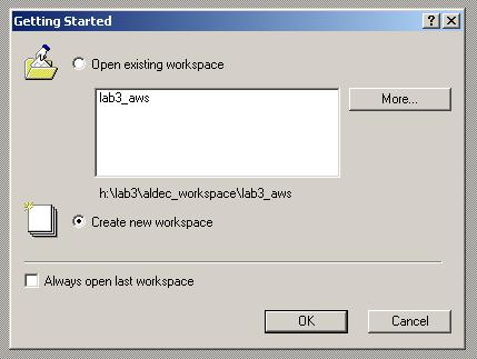
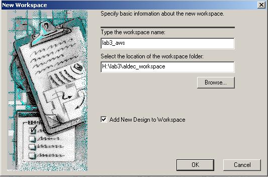
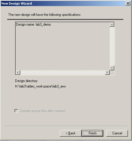
7 Create new workspace and choose Create an Empty Design with Design Flow. Then press Next. You will see a picture similar to the one shown below. 7


8 Verify that Flow Configuration Settings are defined as follows: Synthesis Tool: Xilinx ISE/WebPack <version number> XST Implementation Tool: Xilinx ISE/WebPack <version number> Default Family: Xilinx<version number>x SPARTAN 3 If not, click at the Flow Configuration Settings button and adjust appropriately. 8

9 Also choose, Block Diagram Configuration Default HDL Language Default HDL Language VHDL Once done, select Next Finish 9
10 Now you should see a screen divided into several parts, with a Flow panel on the right side. If you do not see the Flow panel on the right side as shown in the picture, you can press Alt+3 or View Flow from the top menu bar to open the panel. Go to Tools Preferences. In the category expand Tools--> Flow--> integrated tools. Browse to the latest synthesis and implementation tools and select them appropriately. Below example refers to the versions of tools available in the GMU Labs. For home use, you may need to use different versions of tools and program paths. Synthesis tools: 1. Xilinx XST 13.2 (Browse to Xilinx/13.2/ISE/bin/nt/xst.exe) 2. Synplify Premier DP (Select to Snyplify Premier with DP D under category synopsis ) 10

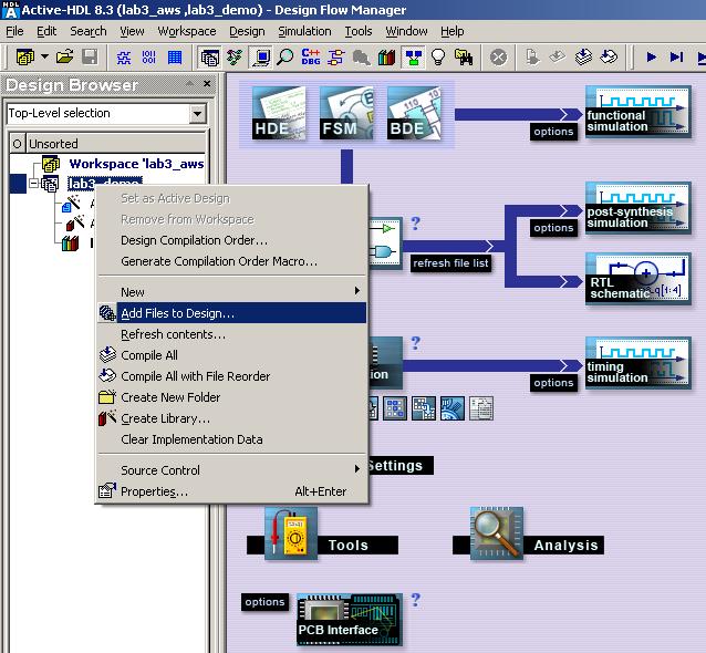
11 Implementation tool: Xilinx XST 13.2 (Browse to Xilinx/13.2/ISE/bin/nt/xst.exe) If the tools for HDL synthesis and implementation are already selected then click on OK. If not, choose the tools as shown above and the path accordingly. Please note that you will be able to select only one synthesis tool at a time. Specify the new design name. Download to your hard drive all VHDL files provided to you at the website for lab3 demo. Add and compile all files from lab3 demo. Then, test your design if it works correctly in the functional simulation as you would normally do. If you are following the tutorial by using lab3demo, make sure you change the slow_clock_period located inside lab3_demo_package.vhd to a number suitable for simulation (5). It will take a long time to simulate otherwise. 11
12 12
13 13

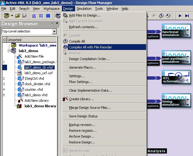
14 Make sure to exclude the.ucf file from compilation. 14
15 15

16 2. Synthesis Synthesis can be done either by using Xilinx XST or Synplify Premier DP. Xilinx XST can be used both at school and at home. Synplify Premier DP is available only at school. 2.1 Synthesis using Xilinx XST Synthesis Options Click at the options button next to the synthesis icon. Under Synthesis Options select Update synthesis order. Arrange your files in the order from the bottom to the top of the design hierarchy. Exclude your non-synthesizable files, such as testbench. Also select a correct Top-level Unit, which is lab3_demo in the example you follow. Make sure that your settings under General tab are as follows: Family : Xilinx<version_number>x SPARTAN3 Device : 3s50pq208 Speed Grade : -4. Under Std Synthesis and Adv Synthesis tabs, you can adjust optimization goal of the synthesis tool for various results. Most notably, you can tell the synthesis tool to optimize for either area or speed. To select either one of them, choose Std Synthesis Optimization Goal select Speed or Area. Click on OK when you are done with option settings. 16

17 Click on the synthesis button and wait until synthesis is completed. 17
18 2.1.2 Synthesis Report Minimum clock period, critical path, and resource utilization can be found from the report file generated after synthesis. To view this file, click on the reports button next to the synthesis icon. Minimum clock period, maximum frequency, and critical path can be found under Timing Summary section. Looking at the critical path can give you an idea which portions of your code to change in order to improve the circuit performance. Resource utilization is located in the Final Report section. Example Report: Resource Utilization 18

19 Example Report: Minimum Clock Period and Critical Path 19
20 2.2 Synthesis using Synplify Premier DP Synthesis Options: Icon to select Design Flow Manager Change the Flow settings in order to select Synplify Premier DP as the primary tool for synthesis. 20

21 Click on options button to select the synthesis options 21


22 Choose lab3_demo as Top-level Unit from the drop down menu Click OK and then click the synthesis button right next to the option button in the Design flow manager. Choose synplifypremierdp as your default license type. 22

23 After applying appropriate settings, click on synthesis in the design flow. You should see the following new window. 23


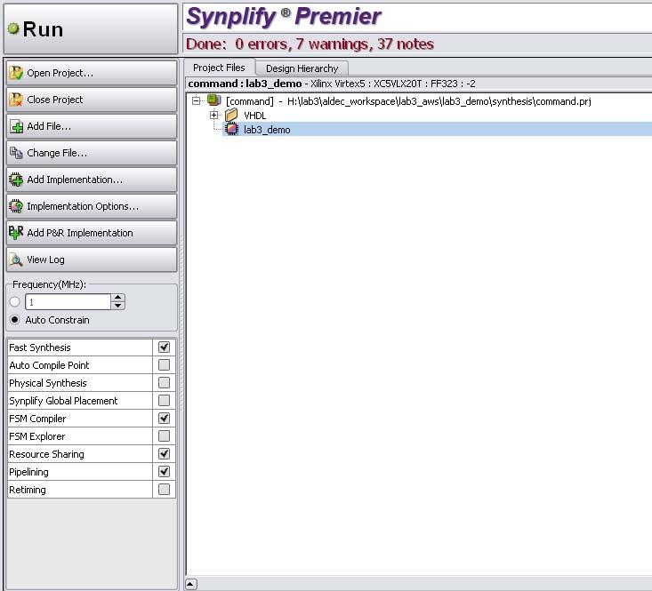
24 There is no need to create a project and adding VHDL source files. Tool will automatically select lab3_demo as default project. Choose the Fast Synthesis option and deselect Physical Synthesis option. Alternatively, double-click lab3_demo to select the appropriate synthesis options. 24

25 Click on Run in the Button panel or select Run from the Run menu. Alternatively, press F8 as the shortcut to this menu. 25
26 26

27 After synthesis, Synplify Premier DP will generate the netlist file lab3_demo.edf in the synthesis folder under the path..\synthesis\lab3_demo. This file is required by Aldec Active-HDL 8.3 for post-synthesis simulation and by Xilinx ISE for implementation. 27


28 2.2.2 Synthesis Report Analyze the results, using report file, the HDL Analyst schematic views, the Message window and the Log Watch window. Log Watch window: Select Compiler Report to analyze the performance summary, timing information, critical path and resource utilization of the design. 28

29 Timing Information: Mapper Report: 29
30 Critical Path Information: Note: Critical path information is also available in HDL Analyst view for better visibility. HDL Analyst schematic views: Select HDL Analyst-> RTL->Hierarchical View or Flattened View to view the design graphically. RTL Hierarchical view: most designs are hierarchical so interactive hierarchical viewing helps to better analyze the design. 30
31 RTL Flattened view: Flattening removes hierarchy so you can view the logic without hierarchy levels. 31

32 Critical path: lab3_demo To generate a view of critical path with Physical analyst tool, click on show critical path (stopwatch icon or select the command from the menu. Example report: Critical path 32
. Then, select Recompile Files.")
33 2.3 Post-Synthesis Simulation Click at the options button next to the post-synthesis simulation icon. Remove the default input file, and select netlist file lab3_demo.edf from synthesis folder and your testbench as an input file by clicking at the button close to the cross sign (marked by a dot). Then, select Recompile Files. Once done, choose the appropriate top-level unit, which is lab3_demo_tb.vhd in this example. Press OK, and then select post-synthesis simulation. Now you should see timing waveforms similar to the ones obtained during functional simulation. The difference is that the components and signals are now mapped into appropriate FPGA hardware. 33

34 3 Implementation 3.1 Implementation Options Browse to synthesis folder and find Netlist file lab3_demo.edf generated after synthesis Browse to user constraint file lab3_demo.ucf, provided in the example Lab 3 Click at the options button next to the implementation icon. Select the correct Netlist File which is a file with the same name as your top level VHDL file and the extension.edf. It is normally located in the synthesis folder of your workspace. Use this file to implement your design. Choose the correct FPGA Family, Device and Speed Grade, the same as used during the Synthesis phase: 34

35 In our example these should be (please ignore values given in the screen shot above): Family : Xilinx<version_number>x SPARTAN3 Device : 3s50pq208 Speed Grade : -4. Under Constraint File, select Custom constraint file. Browse to your.ucf for the lab, lab3_demo.ucf in our example. Then, navigate to the BitStream tab by clicking at the right arrow at the top right hand corner. Under General tab of BitStream deselect Do Not Run Bitgen. This will create bitstream,.bit, which you can upload to FPGA. Additionally, under Post-Map STR, Post-PAR STR, and Simulation tabs make sure that your device speed grade is set to 4. 35

36 You can also specify the implementation tool to use a certain optimization goal. To do this, go to Advanced Map Optimization Goal select either Area or Speed. Press OK, and then select implementation. 36

37 3.2 Implementation Reports Analysis Similarly to synthesis, you can access the generated reports by clicking the reports button, near the implementation icon. Unlike synthesis log, implementation report is divided into several smaller reports, which are named differently. Below is a list of reports in which you can find the most useful information about your design after implementation, such as resource utilization, maximum clock frequency, and critical path: 37


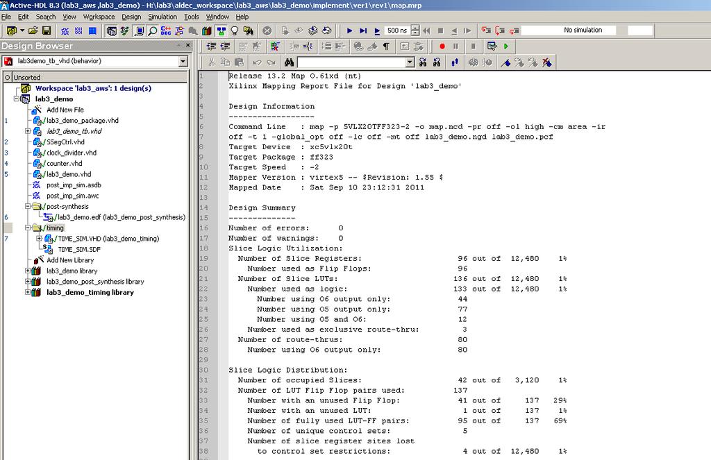
38 Resource Utilization: Map : See Design Summary Place & Route : See Device Utilization Summary Note: Place & Route provides overall information about the design after placing and routing. Map provides a more detailed summary of resource utilization. Minimum Clock Period (Maximum Frequency): Post-Place & Route Static Timing Report This file describes the worst case scenario in terms of minimum clock period. However, since the implementation tools do not provide complete information, please refer to Timing Analysis below for a more detailed report. Note: Post-Map Static Timing Report can be ignored because it provides timing report before placing & routing, and thus cannot correctly predict interconnect delays. 38
39 39

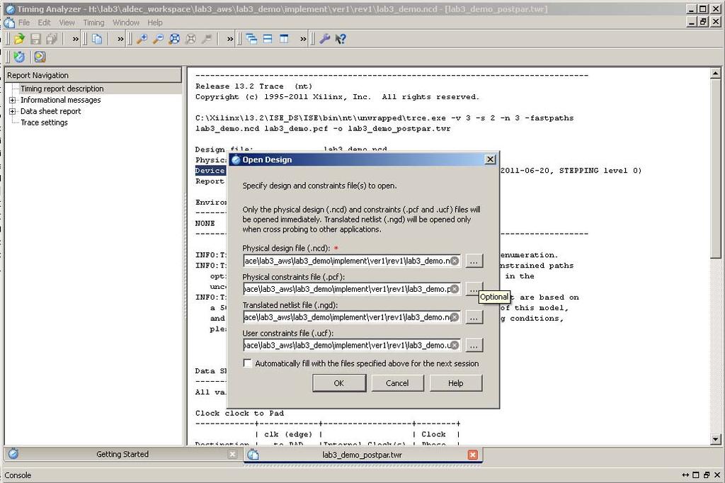
40 Timing Analysis (Clock Period, Maximum Frequency and Critical Path) For the detailed analysis of critical path and minimum clock period (or maximum frequency) a separate timing analyzer provided by Xilinx should be used. To generate the report, select Analysis Static Timing Analyzer from the Flow panel. This will open Xilinx Timing Analyzer. You can also navigate to the program from the Windows menu. The path used in the ECE labs at GMU is by Start All Programs VLSI Tools Xilinx ISE Accessories Timing Analyzer. Once the program is opened, select Open, choose netlist file located in /implement/ver1/rev1 of your workspace, *.ncd, and press OK. Selecting Analyze against Auto Generated Design Constraints will generate a static timing report. 40
41 41
42 42
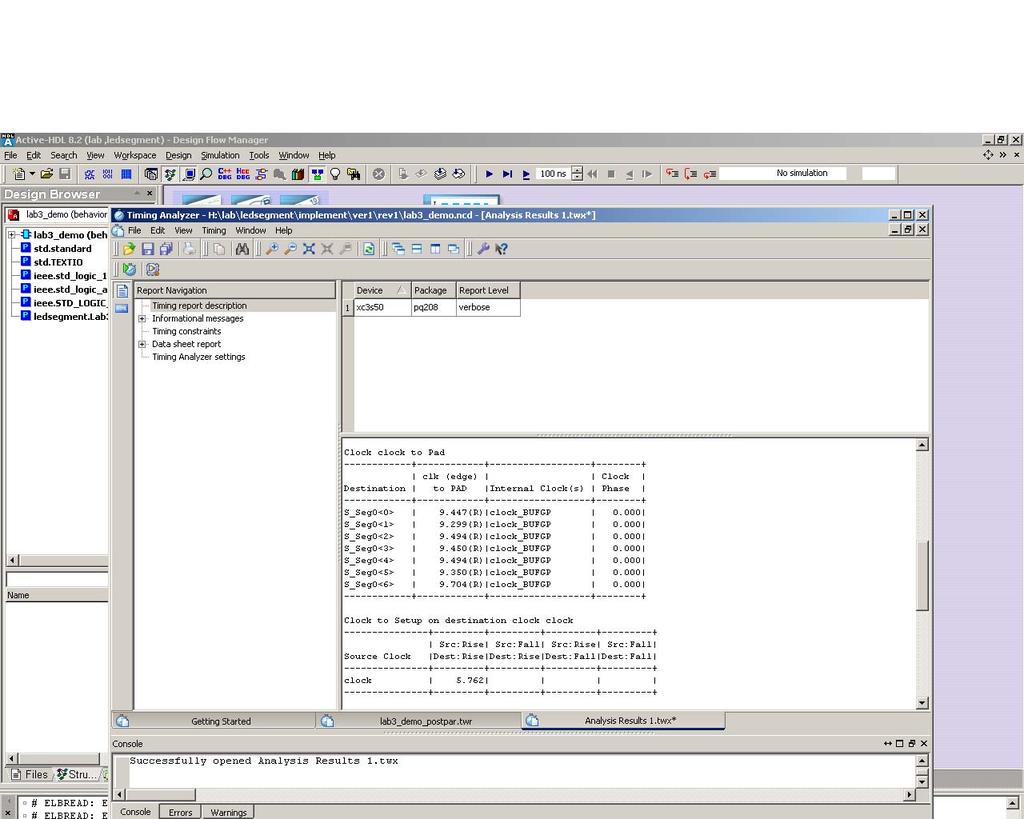
43 Example Report: Clock period, Maximum Frequency and Critical Path. 43

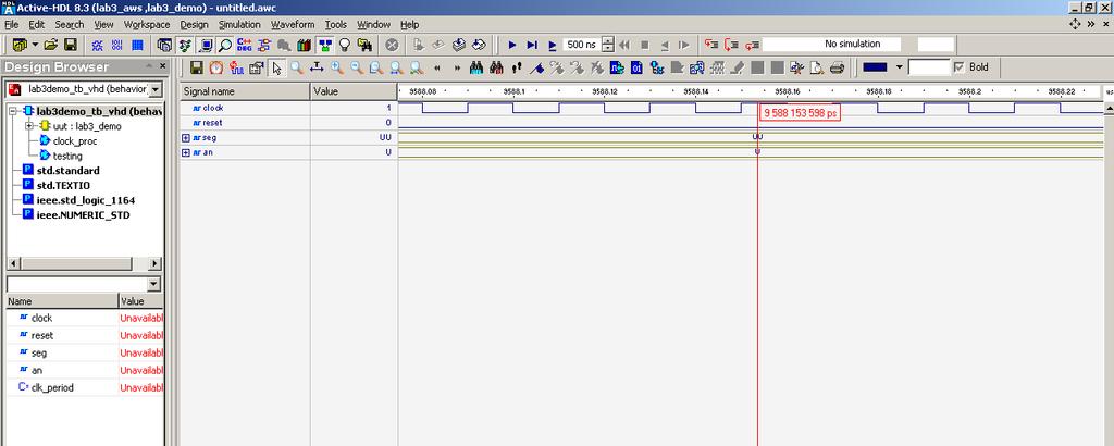
44 3.3 Timing Simulation Browse to implementation folder folder and find TIME_SIM.SDF file generated after implementation Click at the options button next to the timing simulation icon. Select your testbench as the Top-Level Unit. Afterwards, select timing simulation, which will generate timing waveforms based on your netlist after implementation. You should notice slight timing delays compared to the waveforms from your postsynthesis simulation & functional simulation. 44
45 45

46 4. Uploading Bitstream to FPGA Board Before uploading Bit file, make sure that you change your constant values in all your files to proper values, and re-synthesize/re-implement all the files. In particular, in our example, please change the value of the constant slow_clock_period in the Lab3Demo_package.vhd. Select the Adept program as shown in the picture above. When the program is opened, a device will be shown if it is connected and recognized. Select the bit file by clicking Browse and finding the appropriate file. Click Program to program the device. 46

47 Good luck! Have fun debugging =) 47
Tutorial on FPGA Design Flow based on Aldec Active HDL. ver 1.7
 Tutorial on FPGA Design Flow based on Aldec Active HDL ver 1.7 Fall 2012 1 Prepared by Ekawat (Ice) Homsirikamol, Marcin Rogawski, Jeremy Kelly, Kishore Kumar Surapathi, Ambarish Vyas, Malik Umar Sharif
Tutorial on FPGA Design Flow based on Aldec Active HDL. Ver 1.5
 Tutorial on FPGA Design Flow based on Aldec Active HDL Ver 1.5 1 Prepared by Ekawat (Ice) Homsirikamol, Marcin Rogawski, Jeremy Kelly, Kishore Kumar Surapathi and Dr. Kris Gaj This tutorial assumes that
Tutorial on FPGA Design Flow based on Aldec Active HDL. Ver 1.5
 Tutorial on FPGA Design Flow based on Aldec Active HDL Ver 1.5 1 Prepared by Ekawat (Ice) Homsirikamol, Marcin Rogawski, Jeremy Kelly, John Pham, and Dr. Kris Gaj This tutorial assumes that you have basic
Tutorial on FPGA Design Flow based on Xilinx ISE Webpack and ModelSim. ver. 1.5
 Tutorial on FPGA Design Flow based on Xilinx ISE Webpack and ModelSim ver. 1.5 1 Prepared by Marcin Rogawski, Ekawat (Ice) Homsirikamol, Kishore Kumar Surapathi and Dr. Kris Gaj The example codes used
Tutorial on FPGA Design Flow based on Xilinx ISE WebPack and ModelSim. ver. 2.0
 Tutorial on FPGA Design Flow based on Xilinx ISE WebPack and ModelSim ver. 2.0 Updated: Fall 2013 1 Preparing the Input: Download examples associated with this tutorial posted at http://ece.gmu.edu/tutorials-and-lab-manuals
Tutorial on FPGA Design Flow based on Xilinx ISE Webpack and ModelSim. ver. 1.3
 Tutorial on FPGA Design Flow based on Xilinx ISE Webpack and ModelSim ver. 1.3 1 Prepared by Marcin Rogawski, Ekawat (Ice) Homsirikamol, Kishorekum Surapathi, and Dr. Kris Gaj The example codes used in
Tutorial on FPGA Design Flow based on Xilinx ISE Webpack andisim. ver. 1.0
 Tutorial on FPGA Design Flow based on Xilinx ISE Webpack andisim ver. 1.0 1 Prepared by Malik Umar Sharif and Dr. Kris Gaj The example codes used in this tutorial can be obtained from http://ece.gmu.edu/coursewebpages/ece/ece448/s11/labs/448_lab3.htm
Using Synplify Pro, ISE and ModelSim
 Using Synplify Pro, ISE and ModelSim VLSI Systems on Chip ET4 351 Rene van Leuken Huib Lincklaen Arriëns Rev. 1.2 The EDA programs that will be used are: For RTL synthesis: Synplicity Synplify Pro For
ECE 4305 Computer Architecture Lab #1
 ECE 4305 Computer Architecture Lab #1 The objective of this lab is for students to familiarize with the FPGA prototyping system board (Nexys-2) and the Xilinx software development environment that will
EE 1315 DIGITAL LOGIC LAB EE Dept, UMD
 EE 1315 DIGITAL LOGIC LAB EE Dept, UMD EXPERIMENT # 1: Logic building blocks The main objective of this experiment is to let you familiarize with the lab equipment and learn about the operation of the
Xilinx Tutorial Basic Walk-through
 Introduction to Digital Logic Design with FPGA s: Digital logic circuits form the basis of all digital electronic devices. FPGAs (Field Programmable Gate Array) are large programmable digital electronic
Timing Analysis in Xilinx ISE
 Timing Analysis in Xilinx ISE For each design which is to be implemented, constraints should be defined to get predictable results. The first important class of constraints was already introduced in the
and 32 bit for 32 bit. If you don t pay attention to this, there will be unexpected behavior in the ISE software and thing may not work properly!
 This tutorial will show you how to: Part I: Set up a new project in ISE 14.7 Part II: Implement a function using Schematics Part III: Simulate the schematic circuit using ISim Part IV: Constraint, Synthesize,
Xilinx Project Navigator Reference Guide
 31 July 2003 Author: David M. Sendek Xilinx Project Navigator Reference Guide Background: This guide provides you with step-by-step procedures in using the Xilinx Project Navigator to perform the following:
AccelDSP tutorial 2 (Matlab.m to HDL for Xilinx) Ronak Gandhi Syracuse University Fall
 Ronak Gandhi Syracuse University Fall") AccelDSP tutorial 2 (Matlab.m to HDL for Xilinx) Ronak Gandhi Syracuse University Fall 2009-10 AccelDSP Getting Started Tutorial Introduction This tutorial exercise will guide you through the process of
AccelDSP tutorial 2 (Matlab.m to HDL for Xilinx) Ronak Gandhi Syracuse University Fall 2009-10 AccelDSP Getting Started Tutorial Introduction This tutorial exercise will guide you through the process of
FPGA Design Flow 1. All About FPGA
 FPGA Design Flow 1 In this part of tutorial we are going to have a short intro on FPGA design flow. A simplified version of FPGA design flow is given in the flowing diagram. FPGA Design Flow 2 FPGA_Design_FLOW
Circuit Design and Simulation with VHDL 2nd edition Volnei A. Pedroni MIT Press, 2010 Book web:
 Circuit Design and Simulation with VHDL 2nd edition Volnei A. Pedroni MIT Press, 2010 Book web: www.vhdl.us Appendix C Xilinx ISE Tutorial (ISE 11.1) This tutorial is based on ISE 11.1 WebPack (free at
Circuit design with configurable devices (FPGA)
") 1 Material Circuit design with configurable devices (FPGA) Computer with Xilinx's ISE software installed. Digilent's Basys2 prototype board and documentation. Sample design files (lab kit). Files and documents
1 Material Circuit design with configurable devices (FPGA) Computer with Xilinx's ISE software installed. Digilent's Basys2 prototype board and documentation. Sample design files (lab kit). Files and documents
ELEC 204 Digital System Design LABORATORY MANUAL
 ELEC 204 Digital System Design LABORATORY MANUAL : Introductory Tutorial For Xilinx ISE Foundation v10.1 & Implementing XOR Gate College of Engineering Koç University Important Note: In order to effectively
Tutorial: Working with Verilog and the Xilinx FPGA in ISE 9.2i
 Tutorial: Working with Verilog and the Xilinx FPGA in ISE 9.2i This tutorial will show you how to: Use Verilog to specify a design Simulate that Verilog design Define pin constraints for the FPGA (.ucf
4. Verify that HDL is selected as the Top-Level Source Type, and click Next. The New Project Wizard Device Properties page appears.
 Working with the GODIL Author: Ruud Baltissen Credits: Michael Randelzhofer, Ed Spittles Date: August 2010 What is it? This document describes a way to get familiar with the Xilinx FPGAs on OHO s Godil,
Laboratory #Intro to Xilinx ISE and CR-2 Kit ECE 332
 Name: G Number: 1 Introduction Laboratory #Intro to Xilinx ISE and CR-2 Kit ECE 332 The purpose of this laboratory is to introduce the design tools used in ECE 332 lab. In this lab you will learn about
EE 367 Logic Design Lab #1 Introduction to Xilinx ISE and the ML40X Eval Board Date: 1/21/09 Due: 1/28/09
 EE 367 Logic Design Lab #1 Introduction to Xilinx ISE and the ML40X Eval Board Date: 1/21/09 Due: 1/28/09 Lab Description Today s lab will introduce you to the Xilinx Integrated Software Environment (ISE)
VIVADO TUTORIAL- TIMING AND POWER ANALYSIS
 VIVADO TUTORIAL- TIMING AND POWER ANALYSIS IMPORTING THE PROJECT FROM ISE TO VIVADO Initially for migrating the same project which we did in ISE 14.7 to Vivado 2016.1 you will need to follow the steps
Tutorial: ISE 12.2 and the Spartan3e Board v August 2010
 Tutorial: ISE 12.2 and the Spartan3e Board v12.2.1 August 2010 This tutorial will show you how to: Use a combination of schematics and Verilog to specify a design Simulate that design Define pin constraints
Nexys 2 board tutorial (Decoder, ISE 12.2) Jim Duckworth, August 2010, WPI. Digilent Adept Programming Steps added by Zoe (Zhu Fu)
 Jim Duckworth, August 2010, WPI. Digilent Adept Programming Steps added by Zoe (Zhu Fu)") Nexys 2 board tutorial (Decoder, ISE 12.2) Jim Duckworth, August 2010, WPI. Digilent Adept Programming Steps added by Zoe (Zhu Fu) Note: you will need the Xlinx ISE Webpack installed on your compuer (or
Nexys 2 board tutorial (Decoder, ISE 12.2) Jim Duckworth, August 2010, WPI. Digilent Adept Programming Steps added by Zoe (Zhu Fu) Note: you will need the Xlinx ISE Webpack installed on your compuer (or
Revision: February 27, E Main Suite D Pullman, WA (509) Voice and Fax
 Voice and Fax") Xilinx ISE WebPACK VHDL Tutorial Revision: February 27, 2010 215 E Main Suite D Pullman, WA 99163 (509) 334 6306 Voice and Fax Overview This tutorial provides simple instruction for using the Xilinx ISE
Xilinx ISE WebPACK VHDL Tutorial Revision: February 27, 2010 215 E Main Suite D Pullman, WA 99163 (509) 334 6306 Voice and Fax Overview This tutorial provides simple instruction for using the Xilinx ISE
Quick Front-to-Back Overview Tutorial
 Quick Front-to-Back Overview Tutorial PlanAhead Design Tool This tutorial document was last validated using the following software version: ISE Design Suite 14.5 If using a later software version, there
Revision: February 27, E Main Suite D Pullman, WA (509) Voice and Fax
 Voice and Fax") Xilinx ISE WebPACK Schematic Capture Tutorial Revision: February 27, 2010 215 E Main Suite D Pullman, WA 99163 (509) 334 6306 Voice and Fax Overview This tutorial provides instruction for using the Xilinx
Xilinx ISE WebPACK Schematic Capture Tutorial Revision: February 27, 2010 215 E Main Suite D Pullman, WA 99163 (509) 334 6306 Voice and Fax Overview This tutorial provides instruction for using the Xilinx
Lab 1: Introduction to Verilog HDL and the Xilinx ISE
 EE 231-1 - Fall 2016 Lab 1: Introduction to Verilog HDL and the Xilinx ISE Introduction In this lab simple circuits will be designed by programming the field-programmable gate array (FPGA). At the end
Tutorial on Simulation using Aldec Active-HDL Ver 1.0
 Tutorial on Simulation using Aldec Active-HDL Ver 1.0 by Shashi Karanam Introduction Active- HDL is an integrated environment designed for development of VHDL designs. The core of the system is a VHDL
TLL5000 Electronic System Design Base Module
 TLL5000 Electronic System Design Base Module The Learning Labs, Inc. Copyright 2007 Manual Revision 2007.12.28 1 Copyright 2007 The Learning Labs, Inc. Copyright Notice The Learning Labs, Inc. ( TLL )
Xilinx ISE/WebPack: Introduction to Schematic Capture and Simulation
 Xilinx ISE/WebPack: Introduction to Schematic Capture and Simulation Revision: February 7, 2003 Overview This document is intended to assist new entry-level users of the Xilinx ISE/WebPack software. It
PlanAhead Release Notes
 PlanAhead Release Notes What s New in the 11.1 Release UG656(v 11.1.0) April 27, 2009 PlanAhead 11.1 Release Notes Page 1 Table of Contents What s New in the PlanAhead 11.1 Release... 4 Device Support...
Lab 3 Finite State Machines Movie Ticket Dispensing Machine
 Lab 3 Finite State Machines Movie Ticket Dispensing Machine Design, implement, verify, and test a Movie Ticket Dispensing Machine based on the following specification: The machine should allow the choice
ELEC 4200 Lab#0 Tutorial
 1 ELEC 4200 Lab#0 Tutorial Objectives(1) In this Lab exercise, we will design and implement a 2-to-1 multiplexer (MUX), using Xilinx Vivado tools to create a VHDL model of the design, verify the model,
TLL5000 Electronic System Design Base Module. Getting Started Guide, Ver 3.4
 TLL5000 Electronic System Design Base Module Getting Started Guide, Ver 3.4 COPYRIGHT NOTICE The Learning Labs, Inc. ( TLL ) All rights reserved, 2008 Reproduction in any form without permission is prohibited.
ANADOLU UNIVERSITY DEPARTMENT OF ELECTRICAL AND ELECTRONICS ENGINEERING. EEM Digital Systems II
 ANADOLU UNIVERSITY DEPARTMENT OF ELECTRICAL AND ELECTRONICS ENGINEERING EEM 334 - Digital Systems II LAB 1 - INTRODUCTION TO XILINX ISE SOFTWARE AND FPGA 1. PURPOSE In this lab, after you learn to use
Tutorial: Working with the Xilinx tools 14.4
 Tutorial: Working with the Xilinx tools 14.4 This tutorial will show you how to: Part I: Set up a new project in ISE Part II: Implement a function using Schematics Part III: Implement a function using
Introduction. In this exercise you will:
 Introduction In a lot of digital designs (DAQ, Trigger,..) the FPGAs are used. The aim of this exercise is to show you a way to logic design in a FPGA. You will learn all the steps from the idea to the
ECT 224: Digital Computer Fundamentals Using Xilinx StateCAD
 ECT 224: Digital Computer Fundamentals Using Xilinx StateCAD 1) Sequential circuit design often starts with a problem statement tat can be realized in the form of a state diagram or state table a) Xilinx
FPGA Design Tutorial
 ECE 554 Digital Engineering Laboratory FPGA Design Tutorial Version 5.0 Fall 2006 Updated Tutorial: Jake Adriaens Original Tutorial: Matt King, Surin Kittitornkun and Charles R. Kime Table of Contents
ECE 491 Laboratory 1 Introducing FPGA Design with Verilog September 6, 2004
 Goals ECE 491 Laboratory 1 Introducing FPGA Design with Verilog September 6, 2004 1. To review the use of Verilog for combinational logic design. 2. To become familiar with using the Xilinx ISE software
Getting started with the Xilinx Project Navigator and the Digilent BASYS 2 board.
 Getting started with the Xilinx Project Navigator and the Digilent BASYS 2 board. This lab is based on: Xilinx Project Navigator, Release Version 14.6 Digilent Adept System Rev 2.7, Runtime Rev 2.16 Digilent
Nexys 2/3 board tutorial (Decoder, ISE 13.2) Jim Duckworth, August 2011, WPI. (updated March 2012 to include Nexys2 board)
 Jim Duckworth, August 2011, WPI. (updated March 2012 to include Nexys2 board)") Nexys 2/3 board tutorial (Decoder, ISE 13.2) Jim Duckworth, August 2011, WPI. (updated March 2012 to include Nexys2 board) Note: you will need the Xilinx ISE Webpack installed on your computer (or you
Nexys 2/3 board tutorial (Decoder, ISE 13.2) Jim Duckworth, August 2011, WPI. (updated March 2012 to include Nexys2 board) Note: you will need the Xilinx ISE Webpack installed on your computer (or you
Evaluation of the RTL Synthesis Tools for FPGA/PLD Design. M.Matveev. Rice University. August 10, 2001
 Evaluation of the RTL Synthesis Tools for FPGA/PLD Design M.Matveev Rice University August 10, 2001 Xilinx: Foundation ISE Design Entry: VHDL, Verilog, schematic, ABEL Synthesis: Xilinx XST, Synopsys FPGA
Simulation Lab 7 Use ISE to Auto-Generate Testbench Simulations
 Simulation Lab 7 Use ISE to Auto-Generate Testbench Simulations National Science Foundation Funded in part, by a grant from the National Science Foundation DUE 1003736 and 1068182 Step 1: steps should
ISE Design Suite Software Manuals and Help
 ISE Design Suite Software Manuals and Help These documents support the Xilinx ISE Design Suite. Click a document title on the left to view a document, or click a design step in the following figure to
EE183 LAB TUTORIAL. Introduction. Projects. Design Entry
 EE183 LAB TUTORIAL Introduction You will be using several CAD tools to implement your designs in EE183. The purpose of this lab tutorial is to introduce you to the tools that you will be using, Xilinx
Actel Libero TM Integrated Design Environment v2.3 Structural Schematic Flow Design Tutorial
 Actel Libero TM Integrated Design Environment v2.3 Structural Schematic Flow Design Tutorial 1 Table of Contents Design Flow in Libero TM IDE v2.3 Step 1 - Design Creation 3 Step 2 - Design Verification
Lab 3 Sequential Logic for Synthesis. FPGA Design Flow.
 Lab 3 Sequential Logic for Synthesis. FPGA Design Flow. Task 1 Part 1 Develop a VHDL description of a Debouncer specified below. The following diagram shows the interface of the Debouncer. The following
Active-HDL. Getting Started
 Active-HDL Getting Started Active-HDL is an integrated environment designed for development of VHDL designs. The core of the system is a VHDL simulator. Along with debugging and design entry tools, it
1. Downloading. 2. Installation and License Acquiring. Xilinx ISE Webpack + Project Setup Instructions
 Xilinx ISE Webpack + Project Setup Instructions 1. Downloading The Xilinx tools are free for download from their website and can be installed on your Windowsbased PC s. Go to the following URL: http://www.xilinx.com/support/download/index.htm
Digital Circuit Design Using Xilinx ISE Tools
 Digital Circuit Design Using Xilinx ISE Tools Poras T. Balsara and Prashant Vallur Table of Contents 1. Introduction 2. Programmable logic devices: FPGA and CPLD 3. Creating a new project in Xilinx Foundation
Programming Xilinx SPARTAN 3 Board (Simulation through Implementation)
") Programming Xilinx SPARTAN 3 Board (Simulation through Implementation) September 2008 Prepared by: Oluwayomi Adamo Class: Project IV University of North Texas FPGA Physical Description 4 1. VGA (HD-15)
Programming Xilinx SPARTAN 3 Board (Simulation through Implementation) September 2008 Prepared by: Oluwayomi Adamo Class: Project IV University of North Texas FPGA Physical Description 4 1. VGA (HD-15)
Design a three-input, two-output sequential digital circuit which functions as a digital locking mechanism. LOCK ALARM
 Department of Computing Course 112 Hardware First Year Laboratory Assignment Dates for the session 2005-2006: Hand out Date: 10 th January 2006 Hand in deadline (electronic and written report): 17.00 Monday
Laboratory of Digital Circuits Design: Design, Implementation and Simulation of Digital Circuits Using Programmable Devices
 Internet Engineering Dr. Jarosław Sugier Laboratory of Digital Circuits Design: Design, Implementation and Simulation of Digital Circuits Using Programmable Devices This document presents software packages
Evolution of CAD Tools & Verilog HDL Definition
 Evolution of CAD Tools & Verilog HDL Definition K.Sivasankaran Assistant Professor (Senior) VLSI Division School of Electronics Engineering VIT University Outline Evolution of CAD Different CAD Tools for
Vivado Tutorial. Introduction. Objectives. Procedure
 Lab Workbook Introduction This tutorial guides you through the design flow using Xilinx Vivado software to create a simple digital circuit using VHDL. A typical design flow consists of creating model(s),
Logic Implementation on a Xilinx FPGA using VHDL WWU Linux platform assumed. rev 10/25/16
 1 Logic Implementation on a Xilinx FPGA using VHDL WWU Linux platform assumed. rev 10/25/16 The following is a general outline of steps (i.e. design flow) used to implement a digital system described with
Building Combinatorial Circuit Using Behavioral Modeling Lab
 Building Combinatorial Circuit Using Behavioral Modeling Lab Overview: In this lab you will learn how to model a combinatorial circuit using behavioral modeling style of Verilog HDL. You will model a combinatorial
Engineering 1630 Fall Simulating XC9572XL s on the ENGN1630 CPLD-II Board
 Engineering 1630 Fall 2016 Simulating XC9572XL s on the ENGN1630 CPLD-II Board You will use the Aldec Active-HDL software for the required timing simulation of the XC9572XL CPLD programmable logic chips
Tutorial - Using Xilinx System Generator 14.6 for Co-Simulation on Digilent NEXYS3 (Spartan-6) Board
 Board") Tutorial - Using Xilinx System Generator 14.6 for Co-Simulation on Digilent NEXYS3 (Spartan-6) Board Shawki Areibi August 15, 2017 1 Introduction Xilinx System Generator provides a set of Simulink blocks
Tutorial - Using Xilinx System Generator 14.6 for Co-Simulation on Digilent NEXYS3 (Spartan-6) Board Shawki Areibi August 15, 2017 1 Introduction Xilinx System Generator provides a set of Simulink blocks
Vivado Walkthrough ECGR Fall 2015
 ECGR 2181 - Vivado Walkthrough 1 Vivado Walkthrough ECGR 2181 - Fall 2015 Intro In this walkthrough we re going to go through the process of creating a project, adding sources, writing vhdl, simulating
Chapter 9: Integration of Full ASIP and its FPGA Implementation
 Chapter 9: Integration of Full ASIP and its FPGA Implementation 9.1 Introduction A top-level module has been created for the ASIP in VHDL in which all the blocks have been instantiated at the Register
Logic Implementation on a Xilinx FPGA using VHDL WWU Linux platform assumed. rev 11/01/17
 1 Logic Implementation on a Xilinx FPGA using VHDL WWU Linux platform assumed. rev 11/01/17 The following is a general outline of steps (i.e. design flow) used to implement a digital system described with
FPGA Design Flow. - from HDL to physical implementation - Victor Andrei. Kirchhoff-Institut für Physik (KIP) Ruprecht-Karls-Universität Heidelberg
 Ruprecht-Karls-Universität Heidelberg") FPGA Design Flow - from HDL to physical implementation - Victor Andrei Kirchhoff-Institut für Physik (KIP) Ruprecht-Karls-Universität Heidelberg 6th Detector Workshop of the Helmholtz Alliance Physics
FPGA Design Flow - from HDL to physical implementation - Victor Andrei Kirchhoff-Institut für Physik (KIP) Ruprecht-Karls-Universität Heidelberg 6th Detector Workshop of the Helmholtz Alliance Physics
Getting Started with Xilinx WebPack 13.1
 Getting Started with Xilinx WebPack 13.1 B. Ackland June 2011 (Adapted from S. Tewksbury notes WebPack 7.1) This tutorial is designed to help you to become familiar with the operation of the WebPack software
CECS LAB 1 Introduction to Xilinx EDA Tools
 NAME: DUE DATE: STUDENT ID: POSSIBLE POINTS: 10 COURSE DATE & TIME: OBJECTIVE: To familiarize ourselves with the Xilinx Electronic Design Aid (EDA) Tools. We will simulate a simple 4-to-1 Multiplexor using
Vivado Tutorial. Introduction. Objectives. Procedure. Lab Workbook. Vivado Tutorial
 Lab Workbook Introduction This tutorial guides you through the design flow using Xilinx Vivado software to create a simple digital circuit using Verilog HDL. A typical design flow consists of creating
Banks, Jasmine Elizabeth (2011) The Spartan 3E Tutorial 1 : Introduction to FPGA Programming, Version 1.0. [Tutorial Programme]
![Banks, Jasmine Elizabeth (2011) The Spartan 3E Tutorial 1 : Introduction to FPGA Programming, Version 1.0. [Tutorial Programme]](/thumbs/75/72381729.jpg "Banks, Jasmine Elizabeth (2011) The Spartan 3E Tutorial 1 : Introduction to FPGA Programming, Version 1.0. [Tutorial Programme]") QUT Digital Repository: http://eprints.qut.edu.au/ This is the author version published as: This is the accepted version of this article. To be published as : This is the author s version published as:
QUT Digital Repository: http://eprints.qut.edu.au/ This is the author version published as: This is the accepted version of this article. To be published as : This is the author s version published as:
The board is powered by the USB connection, so to turn it on or off you plug it in or unplug it, respectively.
 Lab 1 You may work in pairs or individually on this lab Lab Objectives Learn about the equipment we will be using and how to handle it safely. Learn the basics of using Xilinx ISE to develop hardware designs
XILINX WebPack -- testing with Nexys2 boards at USC (EE201L)
") XILINX WebPack -- testing with Nexys2 boards at USC (EE201L) Gandhi Puvvada 1 Before you start: 1.1 We assume that you have installed WebPACK on your desktop or laptop already. We assume that you have
XILINX WebPack -- testing with Nexys2 boards at USC (EE201L) Gandhi Puvvada 1 Before you start: 1.1 We assume that you have installed WebPACK on your desktop or laptop already. We assume that you have
NIOS CPU Based Embedded Computer System on Programmable Chip
 1 Objectives NIOS CPU Based Embedded Computer System on Programmable Chip EE8205: Embedded Computer Systems This lab has been constructed to introduce the development of dedicated embedded system based
Using the Xilinx CORE Generator in Foundation ISE 3.1i with ModelSim
 Using the Xilinx CORE Generator in Foundation ISE 3.1i with ModelSim Installing Foundation ISE, CORE Generator, and ModelSim Foundation ISE This section explains how to install the Xilinx Foundation ISE
Implementing a Verilog design into the UWEE CPLD Development Board Using Xilinx s ISE 7.1i Software: A Tutorial
 Implementing a Verilog design into the UWEE CPLD Development Board Using Xilinx s ISE 7.1i Software: A Tutorial Revision 0 By: Evan Gander Materials: The following are required in order to complete this
Creating the AVS6LX9MBHP211 MicroBlaze Hardware Platform for the Spartan-6 LX9 MicroBoard Version
 Creating the AVS6LX9MBHP211 MicroBlaze Hardware Platform for the Spartan-6 LX9 MicroBoard Version 13.2.01 Revision History Version Description Date 12.4.01 Initial release for EDK 12.4 09 Mar 2011 12.4.02
ISim Hardware Co-Simulation Tutorial: Accelerating Floating Point FFT Simulation
 ISim Hardware Co-Simulation Tutorial: Accelerating Floating Point FFT Simulation UG817 (v 14.3) October 16, 2012 This tutorial document was last validated using the following software version: ISE Design
Xilinx ChipScope ICON/VIO/ILA Tutorial
 Xilinx ChipScope ICON/VIO/ILA Tutorial The Xilinx ChipScope tools package has several modules that you can add to your Verilog design to capture input and output directly from the FPGA hardware. These
NEXYS4DRR board tutorial
 NEXYS4DRR board tutorial (VHDL Decoder design using Vivado 2015.1) Note: you will need the Xilinx Vivado Webpack version installed on your computer (or you can use the department systems). This tutorial
Lab 6: Intro to FPGAs
 Lab 6: Intro to FPGAs UC Davis Physics 116B Rev 2/22/2018 There s a saying when dealing with complex electronic systems: If you can make the LED blink, you re 90% of the way there., so in this lab you
CPLD Experiment 4. XOR and XNOR Gates with Applications
 CPLD Experiment 4 XOR and XNOR Gates with Applications Based on Xilinx ISE Design Suit 10.1 Department of Electrical & Computer Engineering Florida International University Objectives Materials Examining
Spartan-6 LX9 MicroBoard Embedded Tutorial. Tutorial 1 Creating an AXI-based Embedded System
 Spartan-6 LX9 MicroBoard Embedded Tutorial Tutorial 1 Creating an AXI-based Embedded System Version 13.1.01 Revision History Version Description Date 13.1.01 Initial release for EDK 13.1 5/15/2011 Table
Verilog Design Entry, Synthesis, and Behavioral Simulation
 ------------------------------------------------------------- PURPOSE - This lab will present a brief overview of a typical design flow and then will start to walk you through some typical tasks and familiarize
Revision: February 26, E Main Suite D Pullman, WA (509) Voice and Fax
 Voice and Fax") MCS File Creation with Xilinx ISE Tutorial Revision: February 26, 2010 215 E Main Suite D Pullman, WA 99163 (509) 334 6306 Voice and Fax Overview This tutorial provides instruction for creating an.mcs
MCS File Creation with Xilinx ISE Tutorial Revision: February 26, 2010 215 E Main Suite D Pullman, WA 99163 (509) 334 6306 Voice and Fax Overview This tutorial provides instruction for creating an.mcs
E85: Digital Design and Computer Engineering Lab 2: FPGA Tools and Combinatorial Logic Design
 E85: Digital Design and Computer Engineering Lab 2: FPGA Tools and Combinatorial Logic Design Objective The purpose of this lab is to learn to use Field Programmable Gate Array (FPGA) tools to simulate
Chapter 1. OrCAD/ModelSim Tutorial for CPLDs. Design Description
 Chapter 1 OrCAD/ModelSim Tutorial for CPLDs Design Description This tutorial shows you how to use OrCAD Capture s Schematic module and Express module for compiling XC9500/XL/XV and Xilinx CoolRunner (XCR)
DESIGN STRATEGIES & TOOLS UTILIZED
 CHAPTER 7 DESIGN STRATEGIES & TOOLS UTILIZED 7-1. Field Programmable Gate Array The internal architecture of an FPGA consist of several uncommitted logic blocks in which the design is to be encoded. The
Xilinx ISE Simulation Tutorial
 Xilinx ISE Simulation Tutorial 1. Start Xilinx ISE Project Navigator 2. Create a new project Click on File, then choose New Project on the drop down menu Enter your project name, in this case the project
COS/ELE 375 Verilog & Design Tools Tutorial
 COS/ELE 375 Verilog & Design Tools Tutorial In this tutorial, you will walk through a tutorial using the Xilinx ISE design software with a Digilent Nexys4 DDR FPGA board. In this tutorial, you will learn
Xilinx ISE Synthesis Tutorial
 Xilinx ISE Synthesis Tutorial The following tutorial provides a basic description of how to use Xilinx ISE to create a simple 2-input AND gate and synthesize the design onto the Spartan-3E Starter Board
ISE In-Depth Tutorial. UG695 (v13.1) March 1, 2011
 March 1, 2011") ISE In-Depth Tutorial The information disclosed to you hereunder (the Information ) is provided AS-IS with no warranty of any kind, express or implied. Xilinx does not assume any liability arising from
ISE In-Depth Tutorial The information disclosed to you hereunder (the Information ) is provided AS-IS with no warranty of any kind, express or implied. Xilinx does not assume any liability arising from
Using the ChipScope Pro for Testing HDL Designs on FPGAs
 Using the ChipScope Pro for Testing HDL Designs on FPGAs Compiled by OmkarCK CAD Lab, Dept of E&ECE, IIT Kharagpur. Introduction: Simulation based method is widely used for debugging the FPGA design on
RTL and Technology Schematic Viewers Tutorial. UG685 (v13.1) March 1, 2011
 March 1, 2011") RTL and Technology Schematic Viewers Tutorial The information disclosed to you hereunder (the Information ) is provided AS-IS with no warranty of any kind, express or implied. Xilinx does not assume any
RTL and Technology Schematic Viewers Tutorial The information disclosed to you hereunder (the Information ) is provided AS-IS with no warranty of any kind, express or implied. Xilinx does not assume any
Building an Embedded Processor System on a Xilinx Zync FPGA (Profiling): A Tutorial
: A Tutorial") Building an Embedded Processor System on a Xilinx Zync FPGA (Profiling): A Tutorial Embedded Processor Hardware Design October 6 t h 2017. VIVADO TUTORIAL 1 Table of Contents Requirements... 3 Part 1:
Building an Embedded Processor System on a Xilinx Zync FPGA (Profiling): A Tutorial Embedded Processor Hardware Design October 6 t h 2017. VIVADO TUTORIAL 1 Table of Contents Requirements... 3 Part 1:
Vivado Design Suite User Guide
 Vivado Design Suite User Guide Using the Vivado IDE Notice of Disclaimer The information disclosed to you hereunder (the Materials ) is provided solely for the selection and use of Xilinx products. To
CCE 3202 Advanced Digital System Design
 CCE 3202 Advanced Digital System Design Lab Exercise #2 Introduction You will use Xilinx Webpack v9.1 to allow the synthesis and creation of VHDLbased designs. This lab will outline the steps necessary
CSE 591: Advanced Hardware Design and Verification (2012 Spring) LAB #0
 LAB #0") Lab 0: Tutorial on Xilinx Project Navigator & ALDEC s Active-HDL Simulator CSE 591: Advanced Hardware Design and Verification Assigned: 01/05/2011 Due: 01/19/2011 Table of Contents 1 Overview... 2 1.1
Lab 0: Tutorial on Xilinx Project Navigator & ALDEC s Active-HDL Simulator CSE 591: Advanced Hardware Design and Verification Assigned: 01/05/2011 Due: 01/19/2011 Table of Contents 1 Overview... 2 1.1
Lecture 5: Aldec Active-HDL Simulator
 Lecture 5: Aldec Active-HDL Simulator 1. Objective The objective of this tutorial is to introduce you to Aldec s Active-HDL 9.1 Student Edition simulator by performing the following tasks on a 4-bit adder
An easy to read reference is:
 1. Synopsis: Timing Analysis and Timing Constraints The objective of this lab is to make you familiar with two critical reports produced by the Xilinx ISE during your design synthesis and implementation.