Tutorial on FPGA Design Flow based on Xilinx ISE Webpack andisim. ver. 1.0
|
|
|
- Antonia Collins
- 6 years ago
- Views:
Transcription
1 Tutorial on FPGA Design Flow based on Xilinx ISE Webpack andisim ver
2 Prepared by Malik Umar Sharif and Dr. Kris Gaj The example codes used in this tutorial can be obtained from The current version of the tutorial was tested using the following tools: Toolset Xilinx ISE Webpack Version : 14.2 Synthesis Tool ISE&WebpackSynthesis&Implementation Version : 14.2 Implementation Tool Xilinx ISE/WebPack Version : 14.2 Simulation Tool ISim (Bundled with Xilinx ISE 14.2) 2
3 Table of Contents 1. Project Settings 4 2. Behavioral Simulation Synthesis and Implementation Synthesis with Xilinx XST Synthesis with Synplify Premier DP Translate Post-Translate Simulation Map Place and Route Post Place and Route Simulation Implementation Reports Specifying Frequency/ Time period using User Constraints Optimization strategies Pin Assignment Bit Stream Generation Uploading Bitstream to FPGA Board 33 3

4 1. Project Settings To Start Xilinx ISE in the ECE Labs go to: Start->All Programs-> VLSI Tools->Xilinx ISE <version-number>->ise Design Tools ->Project Navigator At home, adjust the path accordingly based on your installation. To start new Project go to: menu File->New Project 4


5 Specify Project Name and location for project files 5

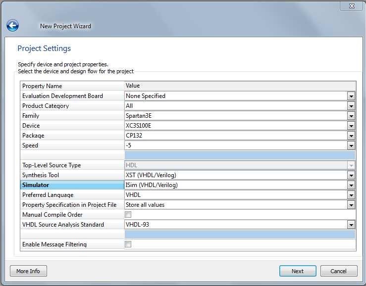
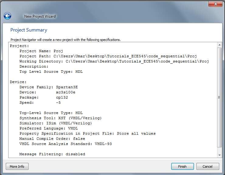
6 Click Nextand specify Family : Xilinx <version number>x Spartan3E Device : XC3S100E Package : cp132 Speed Grade : -5 Simulator : ISim 6
7 7
8 Click Finish and then Add Source. Choose files for the project. 8

9 Then click Ok. Your project has been defined. 9
10 10

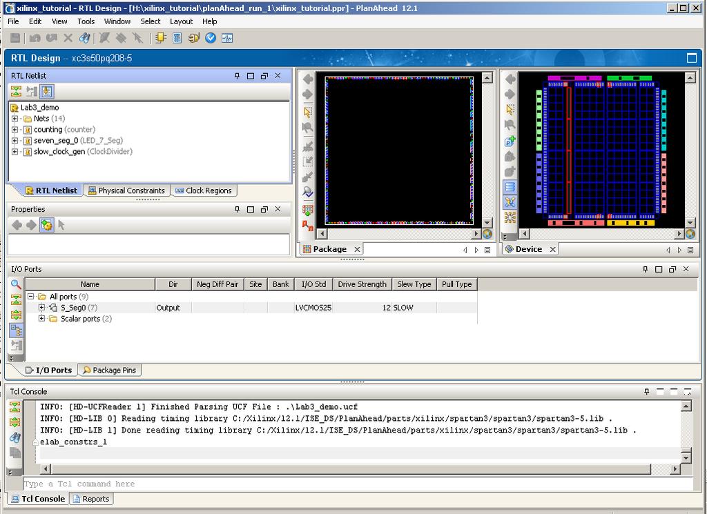
11 2. Behavioral simulation Change the view from Implementation to Simulation by click on the radio button beside simulation.in the Design Menu we choose BehavioralSimulation. The testbench for this design was set as a top level. In the Processes menu choose ISim Simulator, Simulate Behavioral Model, right-click and choose Run. Click on test bench file and it will automatically show the simulator options in the processes window Double click on Simulate Behavioral Model to launch ISim simulator It will launch ISim simulator automatically and waveform for behavioral simulation will appear. 11

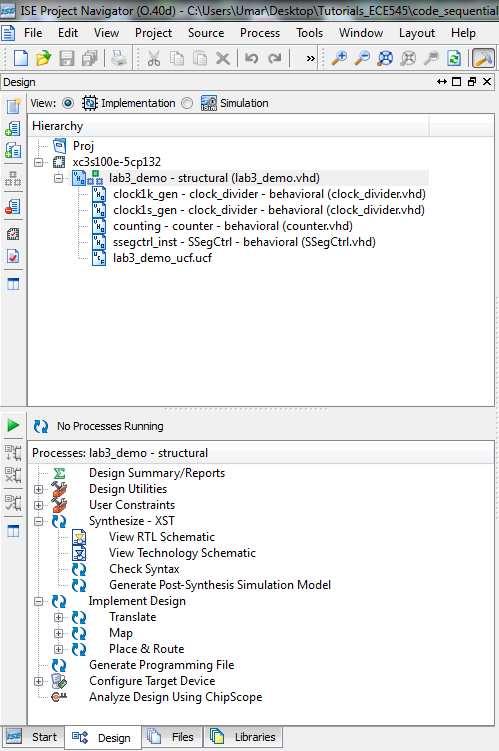
12 3. Synthesis 3.1 Synthesis with Xilinx XST Click on your top-level file (lab3_demo in our case). It will show synthesis and implementation options in the processes window. Click Check Syntaxunder the synthesis option to check if vhdl sources are properly coded. 12

13 After the syntax check is done, double click on synthesis option to synthesize your design. A green tick will appear showing that the synthesis is successfully completed. When Synthesis process is completed, the report from synthesis becomes available. Some of the most important features of the design are the minimum clock period and the maximum clock frequency. We can find these two parameters in the report file from Synthesis. Please remember that the values of these parameters after synthesis are different than the values of the same parameters after implementation.the other important information we can find in this report is the amount of FPGA resources your design requires. 13


14 Generate post-synthesis simulation model by clicking on the option available under synthesis. 14

15 After Synthesis and generation of Post-Synthesis Simulation Model were completed successfully, we can start Implementation part. 3.2 Synthesis with Synplify Premier DP Go to edit menu and click on Preferences. Once a new Preferences window pops up, select Integrated Tools under Category and ISE General option. Set the path for Synplify Premier DP under the synthesis tool "Synplify". Click Apply to save the settings and then click OK. Go to Project menu and click on Design Properties. A new window pops up for Design properties. Go to synthesis tool and click on drop down menu to select Synplify (VHDL). Click OK to save the settings. 15


16 Now you can observe that the synthesis tool changes automatically in the processes menu. Double click on the Synthesize - Synplify to run synthesis using Synplify Premier DP. You can also view RTL and technology view of the schematic. Once you double click on View RTL Schematic, it will automatically invoke the tool "Synplify Premier DP ". 16

17 Finding the Critical path of the design: Click on Run to start the synthesis inside Synplify Premier DP. Click to Technology view icon, followed by Show Critical path button to see the critical path of your design Click to Technology view icon, followed by Show Critical path button to see the critical path of your design 17


18 Go to View menu and click on View Log File. It will open a window and will show you following options: Select compiler report and go down to see the performance summary for the maximum frequency and minimum clock period of the design, estimated after synthesis. Now click on Resource Utilization to see the summary of device utilization in terms of different resources utilized by your design. 18
19 Implementation: Double click on the implementation menu to start the implementation. It will automatically do translate, map and place & route one after the other. Make sure to see the green tick with each option to show that they are successfully completed. 19

20 You can individually run each option (translate, map and place & route) one by one to better understand the design flow. 3.3 Translate The first step in the Xilinx Design Flow for implementation is Translate. Under Implement Designoption, choose Translate, and then Run. If you are successful with this part you should generate Post Translate Simulation Model. 3.4 Post-Translate Simulation Double-click on Generate Post-Translate SimulationModelunder translate option. Change the view from Implementation to Simulation by click on the radio button beside simulation. 20

21 Change Behavioral to Post-Translate option here Click on test bench file. It will automatically show the ISim Simulator under Processes. Double click on the Simulate Post- Translate Model option Double click on the Simulate Post-Translate Model option. It will launch ISim simulator automatically and waveform for post-translate simulation will appear. 3.5 Map Change the view from Simulation toimplementation by click on the radio button beside Implementation. Under 21
22 Implement Design option, double click on Mapto start mapping process. Post-Map Simulation When you right-click on Generate Post-Map SimulationModel then pop-up menu appears. Choose Run to start.change the view from Implementation to Simulation by click on the radio button beside simulation. Change Post- Translate to Post- Map option here Click on test bench file. It will automatically show the ISim Simulator under Processes. Double click on the Simulate Post- Translate Model option Double click on the Simulate Post-Map Model option. It will launch ISim simulator automatically and waveform for post-map simulation will appear. 22
23 23
24 3.6 Place and Route Click on radio button beside Implementation to switch to implementation mode. From the Implement Design menu, choose Place and Route. Double click to start place and route process. After that, double click on Generate Post Place and Route Simulation Model to run it. 3.7 Post Place and Route (Timing) Simulation Double click on Generate Post-Map Simulation Model then pop-up menu appears to run it. Change the view from Implementation to Simulation by click on the radio button beside simulation. Change Post-Mapto Post-Route option here Click on test bench file. It will automatically show the ISim Simulator under Processes. Double click on the Simulate Post-Place & Route Model option Double click on the Simulate Post-Place & Route Model option. It will launch ISim simulator automatically and waveform for post-place & route simulation will appear. 24


25 3.8 Implementation Reports Review the Implementation Reports shown in the following pages. They are available under Design Summary. 25


26 . 4. Specifying Frequency/ Time period using User Constraints: Go to menu Sources for and change this option to Synthesis/Implementation. 4.1 Requesting Synthesis clock frequency: In order to apply timing constraints on the design during the synthesis phase, we specify constraints in.xcf file. Create a new file in any text editor and save it with the extension (.xcf) with the clock period settings as per the design requirement. 26
27 e.g., NET "clk" PERIOD = 3.82 ns; provide the path for synthesis constraint file (.xcf) to include it for synthesis constraints. 4.2 Requesting Implementation clock frequency: In order to apply timing constraints on the design during the implementation phase, we specify constraints in.ucf file. Create a new file in any text editor and save it with the extension (.ucf) with the clock period settings as per the design requirement. e.g., NET "clk" PERIOD = 3.82 ns; Go to Project and click on Add source. Browse and select the.ucf file by giving path to the specific ucf file. Click OK to add the ucf file to the project. 27

28 4.3 Obtaining textual representation of critical path using Timing analyzer (after place & route): Go to Tools menu and then click on Timing Analyzer and select Post Place and Route option. It will automatically include one more tab Timing in the menu. Click on Timing menu and then select Run Analysis Choosing between default (auto-generated) or user-defined constraints: The second setting in the Run Timing Analysis is Analyze again where you can specify through a drop down menu whether you want to specify any constraint on the design or you want to use default (auto-generated) constraint of the tool. As we have already specified the timing constraint in the ucf file for the sample design here, tool will show the constraints that are applied in the ucf file (lab_demo_ucf.ucf). Click OK to see the text report about the timing result after place route. If you have already specified the timing information in the ucf file, choose the default (auto-generated) timing constraints from the tool. 28

29 29 selection between auto-generated and user-defined timing constraints
30 Scroll down till the end of the file (Analysis 1.twx) to see the timing summary that includes minimum period and maximum frequerncy of the design after place and route. As we did not change the Report options, the tool will automatically show the timing information of the paths that have the biggest slack (worst critical path). Search for minimum period in the.twx file from all three paths and choose the one that matches the maximum period shown in the timing summary. It will also have the corresponding critical path information of your design after place and route along with it in the text format. 30
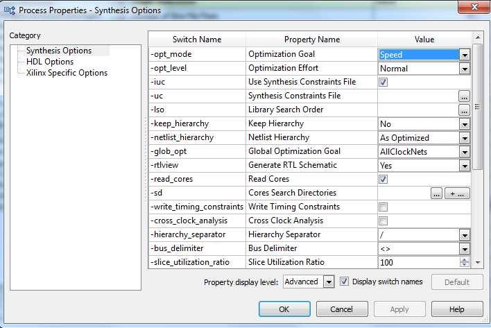
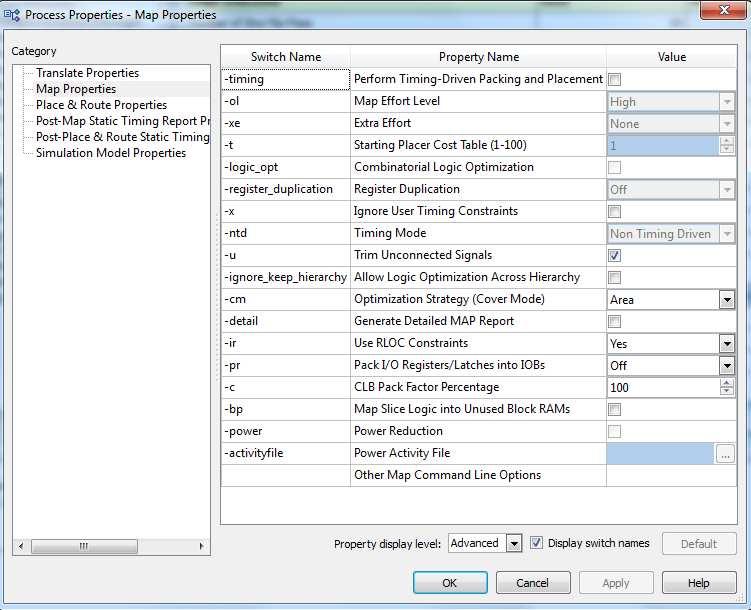
31 5. Optimization strategies: Right click on the synthesis and implemention options in processes menu and then choose process properties to select a complete list of optimization strategies. 31
32 32
. Go to file menu and click on the print menu.")
33 Print the output waveform in PDF format: In order to view all the important details of the behavioral, post-synthesis, post-translate, post-map and post-place & route simulations in waveform in PDF format, use 3rd part tools (PDF creator, PDF Lite etc). Go to file menu and click on the print menu. A pop up will appear that will give you the option to select time range (full range or for a specific range) and an option to fit time range into 1 or multiple pages. Click OK and chose PDF Lite or any other tool to do PDF conversion. After completing the print setup, a new window pops up and ask you to save the file in PDF format. 33


34 Here is the output waveform of post-translate simulation in PDF format. 34
 6.")


35 Note: Remaining two sections apply only to users that target specific FPGA boards (e.g., ECE-448 students) 6. Pin Assignment: Go to menu Sources for and change this option to Synthesis/Implementation. Click on Assign Package Pins. The User Constraint File (UCF) will be created if you decide to assign design port names to the physical pins. Columns I/O Names and I/O Descriptions represent ports from your design. The Loc column should be used to input the location of the corresponding pin in the FPGA device. 35
36 36
.")
37 We can specify Pin Assignments by going to User Constraint menu. We can assign design port names to the physical pins of a chosen device by option Edit Constraints (Text). Keyword NET is for a port name assignment and keyword LOC is for a physical pin assignment. 37

38 7. Bit Stream Generation Go to menu Sources for and change this option to Synthesis/Implementation. Choose Generate Programming File, do right-click and pop-up menu should appear. Choose Run to start bit generation process. 38

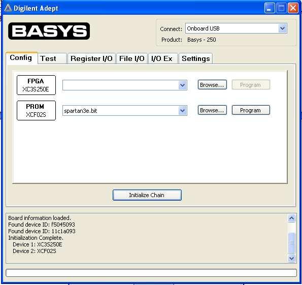
39 8. Uploading Bitstream to FPGA Board Before uploading Bit file, make sure that you change your constant values in all your files to proper values, and re-synthesize/re-implement all the files. In particular, in our example, please change the value of the constant slow_clock_period in the Lab3Demo_package.vhd. Select the Adept program as shown in the picture above. When the program is opened, a device will be shown if it is connected and recognized. Select the bit file by clicking Browse and finding the appropriate file. Click Program to program the file device. 39
40 40
Tutorial on FPGA Design Flow based on Xilinx ISE WebPack and ModelSim. ver. 2.0
 Tutorial on FPGA Design Flow based on Xilinx ISE WebPack and ModelSim ver. 2.0 Updated: Fall 2013 1 Preparing the Input: Download examples associated with this tutorial posted at http://ece.gmu.edu/tutorials-and-lab-manuals
Tutorial on FPGA Design Flow based on Aldec Active HDL. ver 1.7
 Tutorial on FPGA Design Flow based on Aldec Active HDL ver 1.7 Fall 2012 1 Prepared by Ekawat (Ice) Homsirikamol, Marcin Rogawski, Jeremy Kelly, Kishore Kumar Surapathi, Ambarish Vyas, Malik Umar Sharif
Tutorial on FPGA Design Flow based on Xilinx ISE Webpack and ModelSim. ver. 1.5
 Tutorial on FPGA Design Flow based on Xilinx ISE Webpack and ModelSim ver. 1.5 1 Prepared by Marcin Rogawski, Ekawat (Ice) Homsirikamol, Kishore Kumar Surapathi and Dr. Kris Gaj The example codes used
Tutorial on FPGA Design Flow based on Xilinx ISE Webpack and ModelSim. ver. 1.3
 Tutorial on FPGA Design Flow based on Xilinx ISE Webpack and ModelSim ver. 1.3 1 Prepared by Marcin Rogawski, Ekawat (Ice) Homsirikamol, Kishorekum Surapathi, and Dr. Kris Gaj The example codes used in
Tutorial on FPGA Design Flow based on Aldec Active HDL. ver 1.6
 Tutorial on FPGA Design Flow based on Aldec Active HDL ver 1.6 Fall 2011 1 Prepared by Ekawat (Ice) Homsirikamol, Marcin Rogawski, Jeremy Kelly, Kishore Kumar Surapathi, Ambarish Vyas, Umar Sharif and
Tutorial on FPGA Design Flow based on Aldec Active HDL. Ver 1.5
 Tutorial on FPGA Design Flow based on Aldec Active HDL Ver 1.5 1 Prepared by Ekawat (Ice) Homsirikamol, Marcin Rogawski, Jeremy Kelly, Kishore Kumar Surapathi and Dr. Kris Gaj This tutorial assumes that
Tutorial on FPGA Design Flow based on Aldec Active HDL. Ver 1.5
 Tutorial on FPGA Design Flow based on Aldec Active HDL Ver 1.5 1 Prepared by Ekawat (Ice) Homsirikamol, Marcin Rogawski, Jeremy Kelly, John Pham, and Dr. Kris Gaj This tutorial assumes that you have basic
Circuit design with configurable devices (FPGA)
") 1 Material Circuit design with configurable devices (FPGA) Computer with Xilinx's ISE software installed. Digilent's Basys2 prototype board and documentation. Sample design files (lab kit). Files and documents
1 Material Circuit design with configurable devices (FPGA) Computer with Xilinx's ISE software installed. Digilent's Basys2 prototype board and documentation. Sample design files (lab kit). Files and documents
Nexys 2/3 board tutorial (Decoder, ISE 13.2) Jim Duckworth, August 2011, WPI. (updated March 2012 to include Nexys2 board)
 Jim Duckworth, August 2011, WPI. (updated March 2012 to include Nexys2 board)") Nexys 2/3 board tutorial (Decoder, ISE 13.2) Jim Duckworth, August 2011, WPI. (updated March 2012 to include Nexys2 board) Note: you will need the Xilinx ISE Webpack installed on your computer (or you
Nexys 2/3 board tutorial (Decoder, ISE 13.2) Jim Duckworth, August 2011, WPI. (updated March 2012 to include Nexys2 board) Note: you will need the Xilinx ISE Webpack installed on your computer (or you
ECE 4305 Computer Architecture Lab #1
 ECE 4305 Computer Architecture Lab #1 The objective of this lab is for students to familiarize with the FPGA prototyping system board (Nexys-2) and the Xilinx software development environment that will
Programming Xilinx SPARTAN 3 Board (Simulation through Implementation)
") Programming Xilinx SPARTAN 3 Board (Simulation through Implementation) September 2008 Prepared by: Oluwayomi Adamo Class: Project IV University of North Texas FPGA Physical Description 4 1. VGA (HD-15)
Programming Xilinx SPARTAN 3 Board (Simulation through Implementation) September 2008 Prepared by: Oluwayomi Adamo Class: Project IV University of North Texas FPGA Physical Description 4 1. VGA (HD-15)
VIVADO TUTORIAL- TIMING AND POWER ANALYSIS
 VIVADO TUTORIAL- TIMING AND POWER ANALYSIS IMPORTING THE PROJECT FROM ISE TO VIVADO Initially for migrating the same project which we did in ISE 14.7 to Vivado 2016.1 you will need to follow the steps
Getting started with the Xilinx Project Navigator and the Digilent BASYS 2 board.
 Getting started with the Xilinx Project Navigator and the Digilent BASYS 2 board. This lab is based on: Xilinx Project Navigator, Release Version 14.6 Digilent Adept System Rev 2.7, Runtime Rev 2.16 Digilent
Revision: February 27, E Main Suite D Pullman, WA (509) Voice and Fax
 Voice and Fax") Xilinx ISE WebPACK VHDL Tutorial Revision: February 27, 2010 215 E Main Suite D Pullman, WA 99163 (509) 334 6306 Voice and Fax Overview This tutorial provides simple instruction for using the Xilinx ISE
Xilinx ISE WebPACK VHDL Tutorial Revision: February 27, 2010 215 E Main Suite D Pullman, WA 99163 (509) 334 6306 Voice and Fax Overview This tutorial provides simple instruction for using the Xilinx ISE
Circuit Design and Simulation with VHDL 2nd edition Volnei A. Pedroni MIT Press, 2010 Book web:
 Circuit Design and Simulation with VHDL 2nd edition Volnei A. Pedroni MIT Press, 2010 Book web: www.vhdl.us Appendix C Xilinx ISE Tutorial (ISE 11.1) This tutorial is based on ISE 11.1 WebPack (free at
ELEC 204 Digital System Design LABORATORY MANUAL
 ELEC 204 Digital System Design LABORATORY MANUAL : Introductory Tutorial For Xilinx ISE Foundation v10.1 & Implementing XOR Gate College of Engineering Koç University Important Note: In order to effectively
Xilinx ISE Synthesis Tutorial
 Xilinx ISE Synthesis Tutorial The following tutorial provides a basic description of how to use Xilinx ISE to create a simple 2-input AND gate and synthesize the design onto the Spartan-3E Starter Board
Getting Started with Xilinx WebPack 13.1
 Getting Started with Xilinx WebPack 13.1 B. Ackland June 2011 (Adapted from S. Tewksbury notes WebPack 7.1) This tutorial is designed to help you to become familiar with the operation of the WebPack software
Xilinx Project Navigator Reference Guide
 31 July 2003 Author: David M. Sendek Xilinx Project Navigator Reference Guide Background: This guide provides you with step-by-step procedures in using the Xilinx Project Navigator to perform the following:
TLL5000 Electronic System Design Base Module. Getting Started Guide, Ver 3.4
 TLL5000 Electronic System Design Base Module Getting Started Guide, Ver 3.4 COPYRIGHT NOTICE The Learning Labs, Inc. ( TLL ) All rights reserved, 2008 Reproduction in any form without permission is prohibited.
Quick Front-to-Back Overview Tutorial
 Quick Front-to-Back Overview Tutorial PlanAhead Design Tool This tutorial document was last validated using the following software version: ISE Design Suite 14.5 If using a later software version, there
Xilinx ISE8.1 and Spartan-3 Tutorial EE3810
 Xilinx ISE8.1 and Spartan-3 Tutorial EE3810 1 Part1) Starting a new project Simple 3-to-8 Decoder Start the Xilinx ISE 8.1i Project Navigator: Select File > New Project in the opened window 2 Select a
Revision: February 27, E Main Suite D Pullman, WA (509) Voice and Fax
 Voice and Fax") Xilinx ISE WebPACK Schematic Capture Tutorial Revision: February 27, 2010 215 E Main Suite D Pullman, WA 99163 (509) 334 6306 Voice and Fax Overview This tutorial provides instruction for using the Xilinx
Xilinx ISE WebPACK Schematic Capture Tutorial Revision: February 27, 2010 215 E Main Suite D Pullman, WA 99163 (509) 334 6306 Voice and Fax Overview This tutorial provides instruction for using the Xilinx
Logic Implementation on a Xilinx FPGA using VHDL WWU Linux platform assumed. rev 10/25/16
 1 Logic Implementation on a Xilinx FPGA using VHDL WWU Linux platform assumed. rev 10/25/16 The following is a general outline of steps (i.e. design flow) used to implement a digital system described with
CSE 591: Advanced Hardware Design and Verification (2012 Spring) LAB #0
 LAB #0") Lab 0: Tutorial on Xilinx Project Navigator & ALDEC s Active-HDL Simulator CSE 591: Advanced Hardware Design and Verification Assigned: 01/05/2011 Due: 01/19/2011 Table of Contents 1 Overview... 2 1.1
Lab 0: Tutorial on Xilinx Project Navigator & ALDEC s Active-HDL Simulator CSE 591: Advanced Hardware Design and Verification Assigned: 01/05/2011 Due: 01/19/2011 Table of Contents 1 Overview... 2 1.1
Building Combinatorial Circuit Using Behavioral Modeling Lab
 Building Combinatorial Circuit Using Behavioral Modeling Lab Overview: In this lab you will learn how to model a combinatorial circuit using behavioral modeling style of Verilog HDL. You will model a combinatorial
EE 1315 DIGITAL LOGIC LAB EE Dept, UMD
 EE 1315 DIGITAL LOGIC LAB EE Dept, UMD EXPERIMENT # 1: Logic building blocks The main objective of this experiment is to let you familiarize with the lab equipment and learn about the operation of the
Tutorial: Working with the Xilinx tools 14.4
 Tutorial: Working with the Xilinx tools 14.4 This tutorial will show you how to: Part I: Set up a new project in ISE Part II: Implement a function using Schematics Part III: Implement a function using
4. Verify that HDL is selected as the Top-Level Source Type, and click Next. The New Project Wizard Device Properties page appears.
 Working with the GODIL Author: Ruud Baltissen Credits: Michael Randelzhofer, Ed Spittles Date: August 2010 What is it? This document describes a way to get familiar with the Xilinx FPGAs on OHO s Godil,
Logic Implementation on a Xilinx FPGA using VHDL WWU Linux platform assumed. rev 11/01/17
 1 Logic Implementation on a Xilinx FPGA using VHDL WWU Linux platform assumed. rev 11/01/17 The following is a general outline of steps (i.e. design flow) used to implement a digital system described with
TLL5000 Electronic System Design Base Module
 TLL5000 Electronic System Design Base Module The Learning Labs, Inc. Copyright 2007 Manual Revision 2007.12.28 1 Copyright 2007 The Learning Labs, Inc. Copyright Notice The Learning Labs, Inc. ( TLL )
and 32 bit for 32 bit. If you don t pay attention to this, there will be unexpected behavior in the ISE software and thing may not work properly!
 This tutorial will show you how to: Part I: Set up a new project in ISE 14.7 Part II: Implement a function using Schematics Part III: Simulate the schematic circuit using ISim Part IV: Constraint, Synthesize,
Laboratory of Digital Circuits Design: Design, Implementation and Simulation of Digital Circuits Using Programmable Devices
 Internet Engineering Dr. Jarosław Sugier Laboratory of Digital Circuits Design: Design, Implementation and Simulation of Digital Circuits Using Programmable Devices This document presents software packages
Nexys 2 board tutorial (Decoder, ISE 12.2) Jim Duckworth, August 2010, WPI. Digilent Adept Programming Steps added by Zoe (Zhu Fu)
 Jim Duckworth, August 2010, WPI. Digilent Adept Programming Steps added by Zoe (Zhu Fu)") Nexys 2 board tutorial (Decoder, ISE 12.2) Jim Duckworth, August 2010, WPI. Digilent Adept Programming Steps added by Zoe (Zhu Fu) Note: you will need the Xlinx ISE Webpack installed on your compuer (or
Nexys 2 board tutorial (Decoder, ISE 12.2) Jim Duckworth, August 2010, WPI. Digilent Adept Programming Steps added by Zoe (Zhu Fu) Note: you will need the Xlinx ISE Webpack installed on your compuer (or
Laboratory #Intro to Xilinx ISE and CR-2 Kit ECE 332
 Name: G Number: 1 Introduction Laboratory #Intro to Xilinx ISE and CR-2 Kit ECE 332 The purpose of this laboratory is to introduce the design tools used in ECE 332 lab. In this lab you will learn about
Xilinx Tutorial Basic Walk-through
 Introduction to Digital Logic Design with FPGA s: Digital logic circuits form the basis of all digital electronic devices. FPGAs (Field Programmable Gate Array) are large programmable digital electronic
Using Synplify Pro, ISE and ModelSim
 Using Synplify Pro, ISE and ModelSim VLSI Systems on Chip ET4 351 Rene van Leuken Huib Lincklaen Arriëns Rev. 1.2 The EDA programs that will be used are: For RTL synthesis: Synplicity Synplify Pro For
Actel Libero TM Integrated Design Environment v2.3 Structural Schematic Flow Design Tutorial
 Actel Libero TM Integrated Design Environment v2.3 Structural Schematic Flow Design Tutorial 1 Table of Contents Design Flow in Libero TM IDE v2.3 Step 1 - Design Creation 3 Step 2 - Design Verification
Tutorial: Working with Verilog and the Xilinx FPGA in ISE 9.2i
 Tutorial: Working with Verilog and the Xilinx FPGA in ISE 9.2i This tutorial will show you how to: Use Verilog to specify a design Simulate that Verilog design Define pin constraints for the FPGA (.ucf
XILINX ISE AND SPARTAN 3AN TUTORIAL
 XILINX ISE AND SPARTAN 3AN TUTORIAL SYNTETIZE AND SIMULATION------------------------------------------ This tutorial will show you how to create a simple Xilinx ISE project based on the Spartan-3 Board.
Lab 1: Introduction to Verilog HDL and the Xilinx ISE
 EE 231-1 - Fall 2016 Lab 1: Introduction to Verilog HDL and the Xilinx ISE Introduction In this lab simple circuits will be designed by programming the field-programmable gate array (FPGA). At the end
EE 367 Logic Design Lab #1 Introduction to Xilinx ISE and the ML40X Eval Board Date: 1/21/09 Due: 1/28/09
 EE 367 Logic Design Lab #1 Introduction to Xilinx ISE and the ML40X Eval Board Date: 1/21/09 Due: 1/28/09 Lab Description Today s lab will introduce you to the Xilinx Integrated Software Environment (ISE)
Tutorial: ISE 12.2 and the Spartan3e Board v August 2010
 Tutorial: ISE 12.2 and the Spartan3e Board v12.2.1 August 2010 This tutorial will show you how to: Use a combination of schematics and Verilog to specify a design Simulate that design Define pin constraints
Xilinx ISE8.1 and Spartan-3 Tutorial (Prepared by Kahraman Akdemir based on Professor Duckworth's Tutorials updated September 2006)
") Xilinx ISE8.1 and Spartan-3 Tutorial (Prepared by Kahraman Akdemir based on Professor Duckworth's Tutorials updated September 2006) 1 Part1) Starting a new project Simple 3-to-8 Decoder Start the Xilinx
Xilinx ISE8.1 and Spartan-3 Tutorial (Prepared by Kahraman Akdemir based on Professor Duckworth's Tutorials updated September 2006) 1 Part1) Starting a new project Simple 3-to-8 Decoder Start the Xilinx
XILINX WebPack -- testing with Nexys2 boards at USC (EE201L)
") XILINX WebPack -- testing with Nexys2 boards at USC (EE201L) Gandhi Puvvada 1 Before you start: 1.1 We assume that you have installed WebPACK on your desktop or laptop already. We assume that you have
XILINX WebPack -- testing with Nexys2 boards at USC (EE201L) Gandhi Puvvada 1 Before you start: 1.1 We assume that you have installed WebPACK on your desktop or laptop already. We assume that you have
Banks, Jasmine Elizabeth (2011) The Spartan 3E Tutorial 1 : Introduction to FPGA Programming, Version 1.0. [Tutorial Programme]
![Banks, Jasmine Elizabeth (2011) The Spartan 3E Tutorial 1 : Introduction to FPGA Programming, Version 1.0. [Tutorial Programme]](/thumbs/75/72381729.jpg "Banks, Jasmine Elizabeth (2011) The Spartan 3E Tutorial 1 : Introduction to FPGA Programming, Version 1.0. [Tutorial Programme]") QUT Digital Repository: http://eprints.qut.edu.au/ This is the author version published as: This is the accepted version of this article. To be published as : This is the author s version published as:
QUT Digital Repository: http://eprints.qut.edu.au/ This is the author version published as: This is the accepted version of this article. To be published as : This is the author s version published as:
CCE 3202 Advanced Digital System Design
 CCE 3202 Advanced Digital System Design Lab Exercise #2 Introduction You will use Xilinx Webpack v9.1 to allow the synthesis and creation of VHDLbased designs. This lab will outline the steps necessary
ECE 491 Laboratory 1 Introducing FPGA Design with Verilog September 6, 2004
 Goals ECE 491 Laboratory 1 Introducing FPGA Design with Verilog September 6, 2004 1. To review the use of Verilog for combinational logic design. 2. To become familiar with using the Xilinx ISE software
AccelDSP tutorial 2 (Matlab.m to HDL for Xilinx) Ronak Gandhi Syracuse University Fall
 Ronak Gandhi Syracuse University Fall") AccelDSP tutorial 2 (Matlab.m to HDL for Xilinx) Ronak Gandhi Syracuse University Fall 2009-10 AccelDSP Getting Started Tutorial Introduction This tutorial exercise will guide you through the process of
AccelDSP tutorial 2 (Matlab.m to HDL for Xilinx) Ronak Gandhi Syracuse University Fall 2009-10 AccelDSP Getting Started Tutorial Introduction This tutorial exercise will guide you through the process of
PlanAhead Release Notes
 PlanAhead Release Notes What s New in the 11.1 Release UG656(v 11.1.0) April 27, 2009 PlanAhead 11.1 Release Notes Page 1 Table of Contents What s New in the PlanAhead 11.1 Release... 4 Device Support...
1. Downloading. 2. Installation and License Acquiring. Xilinx ISE Webpack + Project Setup Instructions
 Xilinx ISE Webpack + Project Setup Instructions 1. Downloading The Xilinx tools are free for download from their website and can be installed on your Windowsbased PC s. Go to the following URL: http://www.xilinx.com/support/download/index.htm
COS/ELE 375 Verilog & Design Tools Tutorial
 COS/ELE 375 Verilog & Design Tools Tutorial In this tutorial, you will walk through a tutorial using the Xilinx ISE design software with a Digilent Nexys4 DDR FPGA board. In this tutorial, you will learn
Verilog Design Entry, Synthesis, and Behavioral Simulation
 ------------------------------------------------------------- PURPOSE - This lab will present a brief overview of a typical design flow and then will start to walk you through some typical tasks and familiarize
Xilinx ISE Simulation Tutorial
 Xilinx ISE Simulation Tutorial 1. Start Xilinx ISE Project Navigator 2. Create a new project Click on File, then choose New Project on the drop down menu Enter your project name, in this case the project
CPLD Experiment 4. XOR and XNOR Gates with Applications
 CPLD Experiment 4 XOR and XNOR Gates with Applications Based on Xilinx ISE Design Suit 10.1 Department of Electrical & Computer Engineering Florida International University Objectives Materials Examining
ECT 224: Digital Computer Fundamentals Using Xilinx StateCAD
 ECT 224: Digital Computer Fundamentals Using Xilinx StateCAD 1) Sequential circuit design often starts with a problem statement tat can be realized in the form of a state diagram or state table a) Xilinx
Xilinx ISE/WebPack: Introduction to Schematic Capture and Simulation
 Xilinx ISE/WebPack: Introduction to Schematic Capture and Simulation Revision: February 7, 2003 Overview This document is intended to assist new entry-level users of the Xilinx ISE/WebPack software. It
FPGA Design Tutorial
 ECE 554 Digital Engineering Laboratory FPGA Design Tutorial Version 5.0 Fall 2006 Updated Tutorial: Jake Adriaens Original Tutorial: Matt King, Surin Kittitornkun and Charles R. Kime Table of Contents
Lab 3 Sequential Logic for Synthesis. FPGA Design Flow.
 Lab 3 Sequential Logic for Synthesis. FPGA Design Flow. Task 1 Part 1 Develop a VHDL description of a Debouncer specified below. The following diagram shows the interface of the Debouncer. The following
VHDL introduction Notes
 UH Hawaii Manoa 475 Electronics for physicists VHDL introduction Notes Author: Andrej Seljak Date: Fall 2016 update 1 Ver: 1.0 Table of Contents 1. FPGA description3 2. USB EVALUATION board 4 3. ISE Xilinx
Implementing a Verilog design into the UWEE CPLD Development Board Using Xilinx s ISE 7.1i Software: A Tutorial
 Implementing a Verilog design into the UWEE CPLD Development Board Using Xilinx s ISE 7.1i Software: A Tutorial Revision 0 By: Evan Gander Materials: The following are required in order to complete this
OVERVIEW OF FPGA AND EDA SOFTWARE
 CHAPTER 2 OVERVIEW OF FPGA AND EDA SOFTWARE 2.1 INTRODUCTION Developing a large FPGA-based system is an involved process that consists of many complex transformations and optimization algorithms. Software
2IN35 VLSI Programming Lab Work Assignment 1: Hardware design using Verilog
 2IN35 VLSI Programming Lab Work Assignment 1: Hardware design using Verilog Hrishikesh Salunkhe, h.l.salunkhe@tue.nl, Alok Lele, a.lele@tue.nl April 28, 2015 1 Contents 1 Introduction 3 2 Hardware design
Xilinx ChipScope ICON/VIO/ILA Tutorial
 Xilinx ChipScope ICON/VIO/ILA Tutorial The Xilinx ChipScope tools package has several modules that you can add to your Verilog design to capture input and output directly from the FPGA hardware. These
ISE Design Suite Software Manuals and Help
 ISE Design Suite Software Manuals and Help These documents support the Xilinx ISE Design Suite. Click a document title on the left to view a document, or click a design step in the following figure to
Introduction. In this exercise you will:
 Introduction In a lot of digital designs (DAQ, Trigger,..) the FPGAs are used. The aim of this exercise is to show you a way to logic design in a FPGA. You will learn all the steps from the idea to the
Lab 3 Finite State Machines Movie Ticket Dispensing Machine
 Lab 3 Finite State Machines Movie Ticket Dispensing Machine Design, implement, verify, and test a Movie Ticket Dispensing Machine based on the following specification: The machine should allow the choice
Lab 3: Xilinx PicoBlaze Flow Lab Targeting Spartan-3E Starter Kit
 Lab 3: Xilinx PicoBlaze Flow Lab Targeting Spartan-3E Starter Kit Xilinx PicoBlaze Flow Demo Lab www.xilinx.com 1-1 Create a New Project Step 1 Create a new project targeting the Spartan-3E device that
An easy to read reference is:
 1. Synopsis: Timing Analysis and Timing Constraints The objective of this lab is to make you familiar with two critical reports produced by the Xilinx ISE during your design synthesis and implementation.
CECS LAB 1 Introduction to Xilinx EDA Tools
 NAME: DUE DATE: STUDENT ID: POSSIBLE POINTS: 10 COURSE DATE & TIME: OBJECTIVE: To familiarize ourselves with the Xilinx Electronic Design Aid (EDA) Tools. We will simulate a simple 4-to-1 Multiplexor using
ELEC 4200 Lab#0 Tutorial
 1 ELEC 4200 Lab#0 Tutorial Objectives(1) In this Lab exercise, we will design and implement a 2-to-1 multiplexer (MUX), using Xilinx Vivado tools to create a VHDL model of the design, verify the model,
University of Hawaii EE 361L. Getting Started with Spartan 3E Digilent Basys2 Board. Lab 4.1
 University of Hawaii EE 361L Getting Started with Spartan 3E Digilent Basys2 Board Lab 4.1 I. Test Basys2 Board Attach the Basys2 board to the PC or laptop with the USB connector. Make sure the blue jumper
Tutorial - Using Xilinx System Generator 14.6 for Co-Simulation on Digilent NEXYS3 (Spartan-6) Board
 Board") Tutorial - Using Xilinx System Generator 14.6 for Co-Simulation on Digilent NEXYS3 (Spartan-6) Board Shawki Areibi August 15, 2017 1 Introduction Xilinx System Generator provides a set of Simulink blocks
Tutorial - Using Xilinx System Generator 14.6 for Co-Simulation on Digilent NEXYS3 (Spartan-6) Board Shawki Areibi August 15, 2017 1 Introduction Xilinx System Generator provides a set of Simulink blocks
Verilog Module Tutorial By TA Brian W. Stevens CMPE415 UMBC Spring 2015 Dr. Tinoosh Mohsenin
 Verilog Module Tutorial By TA Brian W. Stevens CMPE415 UMBC Spring 2015 Dr. Tinoosh Mohsenin What will this guide teach you? This guide will go through how to use Xilinx 13.2 to create a Verilog module
Design a three-input, two-output sequential digital circuit which functions as a digital locking mechanism. LOCK ALARM
 Department of Computing Course 112 Hardware First Year Laboratory Assignment Dates for the session 2005-2006: Hand out Date: 10 th January 2006 Hand in deadline (electronic and written report): 17.00 Monday
DIGITAL LOGIC WITH VHDL (Fall 2013) Unit 1
 Unit 1") DIGITAL LOGIC WITH VHDL (Fall 23) Unit DESIGN FLOW DATA TYPES LOGIC GATES WITH VHDL TESTBENCH GENERATION DESIGN FLOW Design Entry: We specify the logic circuit using a Hardware Description Language (e.g.,
DIGITAL LOGIC WITH VHDL (Fall 23) Unit DESIGN FLOW DATA TYPES LOGIC GATES WITH VHDL TESTBENCH GENERATION DESIGN FLOW Design Entry: We specify the logic circuit using a Hardware Description Language (e.g.,
FPGA Design Flow 1. All About FPGA
 FPGA Design Flow 1 In this part of tutorial we are going to have a short intro on FPGA design flow. A simplified version of FPGA design flow is given in the flowing diagram. FPGA Design Flow 2 FPGA_Design_FLOW
PlanAhead Software Tutorial
 PlanAhead Software Tutorial RTL Design and IP Generation The information disclosed to you hereunder (the Information ) is provided AS-IS with no warranty of any kind, express or implied. Xilinx does not
MANUAL XILINX ISE PROJECT NAVIGATOR
 Hochschule für Angewandte Wissenschaften Hamburg University of Applied Sciences Department of Electrical Engineering and Computer Sciences MANUAL XILINX ISE PROJECT NAVIGATOR AND MODELSIM Design Flow for
Introduction to Verilog and XILINX
 DEPARTAMENTO DE TECNOLOGÍA ELECTRÓNICA ESCUELA TÉCNICA SUPERIOR DE INGENIERÍA INFORMÁTICA Introduction to Verilog and XILINX Lab Session Computer Structure WARNING: A written solution of the preliminary
ENGN 1630: CPLD Simulation Fall ENGN 1630 Fall Simulating XC9572XLs on the ENGN1630 CPLD-II Board Using Xilinx ISim
 ENGN 1630 Fall 2018 Simulating XC9572XLs on the ENGN1630 CPLD-II Board Using Xilinx ISim You will use the Xilinx ISim simulation software for the required timing simulation of the XC9572XL CPLD programmable
Using the ChipScope Pro for Testing HDL Designs on FPGAs
 Using the ChipScope Pro for Testing HDL Designs on FPGAs Compiled by OmkarCK CAD Lab, Dept of E&ECE, IIT Kharagpur. Introduction: Simulation based method is widely used for debugging the FPGA design on
Department of Electrical and Computer Engineering Xilinx ISIM <Release Version: 14.1i> Simulation Tutorial Using Verilog
 Department of Electrical and Computer Engineering Xilinx ISIM Simulation Tutorial Using Verilog Spring 2013 Baback Izadi You will next test the full adder circuit that you built
Programmable Logic Design I
 Programmable Logic Design I Introduction In labs 11 and 12 you built simple logic circuits on breadboards using TTL logic circuits on 7400 series chips. This process is simple and easy for small circuits.
Xilinx Schematic Entry Tutorial
 Overview Xilinx Schematic Entry Tutorial Xilinx ISE Schematic Entry & Modelsim Simulation What is circuit simulation and why is it important? Complex designs, short design cycle Simultaneous system design
Introduction to WebPACK 3.1. Using XILINX WebPACK Software to Create CPLD Designs
 Introduction to WebPACK 3.1 Using XILINX WebPACK Software to Create CPLD Designs RELEASE DATE: 8/28/2000 All XS-prefix product designations are trademarks of XESS Corp. All XC-prefix product designations
Adding the ILA Core to an Existing Design Lab
 Adding the ILA Core to an Existing Introduction This lab consists of adding a ChipScope Pro software ILA core with the Core Inserter tool and debugging a nonfunctioning design. The files for this lab are
ISE Simulator (ISim) In-Depth Tutorial. UG682 (v 13.1) March 1, 2011
 In-Depth Tutorial. UG682 (v 13.1) March 1, 2011") ISE Simulator (ISim) In-Depth Tutorial Xilinx is disclosing this user guide, manual, release note, and/or specification (the "Documentation") to you solely for use in the development of designs to operate
ISE Simulator (ISim) In-Depth Tutorial Xilinx is disclosing this user guide, manual, release note, and/or specification (the "Documentation") to you solely for use in the development of designs to operate
Introduction to WebPACK 8.1. Using Xilinx WebPACK Software to Create FPGA Designs for the XSA Board
 Introduction to WebPACK 8.1 Using Xilinx WebPACK Software to Create FPGA Designs for the XSA Board Release date: 5/16/2005 2006 by XESS Corp. All XS-prefix product designations are trademarks of XESS
RTL Design and IP Generation Tutorial. PlanAhead Design Tool
 RTL Design and IP Generation Tutorial PlanAhead Design Tool Notice of Disclaimer The information disclosed to you hereunder (the "Materials") is provided solely for the selection and use of Xilinx products.
ISim Hardware Co-Simulation Tutorial: Accelerating Floating Point FFT Simulation
 ISim Hardware Co-Simulation Tutorial: Accelerating Floating Point FFT Simulation UG817 (v 14.3) October 16, 2012 This tutorial document was last validated using the following software version: ISE Design
Programmable Logic Design I
 Programmable Logic Design I Read through each section completely before starting so that you have the benefit of all the directions. Put on a grounded wrist strap (cf. Getting Started) before touching
Timing Analysis in Xilinx ISE
 Timing Analysis in Xilinx ISE For each design which is to be implemented, constraints should be defined to get predictable results. The first important class of constraints was already introduced in the
Vivado Design Suite Tutorial. Design Flows Overview
 Vivado Design Suite Tutorial Design Flows Overview Notice of Disclaimer The information disclosed to you hereunder (the "Materials") is provided solely for the selection and use of Xilinx products. To
The board is powered by the USB connection, so to turn it on or off you plug it in or unplug it, respectively.
 Lab 1 You may work in pairs or individually on this lab Lab Objectives Learn about the equipment we will be using and how to handle it safely. Learn the basics of using Xilinx ISE to develop hardware designs
Introduction to WebPACK 5.2 for FPGAs. Using Xilinx WebPACK Software to Create FPGA Designs for the XSB-300E Board
 Introduction to WebPACK 5.2 for FPGAs Using Xilinx WebPACK Software to Create FPGA Designs for the XSB-300E Board Release date: 10/27/2003 All XS-prefix product designations are trademarks of XESS Corp.
WebPACK ISE DESIGN SOFTWARE
 3 WebPACK ISE DESIGN SOFTWARE The WebPACK ISE design software offers a complete design suite based on the Xilinx Foundation ISE series software. This chapter describes how to install the software and what
475 Electronics for physicists Introduction to FPGA programming
 475 Electronics for physicists Introduction to FPGA programming Andrej Seljak, Gary Varner Department of Physics University of Hawaii at Manoa November 18, 2015 Abstract Digital circuits based on binary
Chapter 9: Integration of Full ASIP and its FPGA Implementation
 Chapter 9: Integration of Full ASIP and its FPGA Implementation 9.1 Introduction A top-level module has been created for the ASIP in VHDL in which all the blocks have been instantiated at the Register
Introduction to WebPACK 6.3. Using Xilinx WebPACK Software to Create FPGA Designs for the XSA Board
 Introduction to WebPACK 6.3 Using Xilinx WebPACK Software to Create FPGA Designs for the XSA Board Release date: 1/1/2005 2005 by XESS Corp. All XS-prefix product designations are trademarks of XESS Corp.