Tutorial on FPGA Design Flow based on Xilinx ISE Webpack and ModelSim. ver. 1.5
|
|
|
- Iris McKenzie
- 5 years ago
- Views:
Transcription
1 Tutorial on FPGA Design Flow based on Xilinx ISE Webpack and ModelSim ver
2 Prepared by Marcin Rogawski, Ekawat (Ice) Homsirikamol, Kishore Kumar Surapathi and Dr. Kris Gaj The example codes used in this tutorial can be obtained from The current version of the tutorial was tested using the following tools: Toolset Xilinx ISE Webpack Version : 12.1 Synthesis Tool ISE&Webpack Synthesis&Implementation Version : 12.1 Implementation Tool Xilinx ISE/WebPack Version : 12.1 Simulation Tool ModelSim SE Version : 6.3c 2
3 Table of Contents 1. Project Settings 4 2. Behavioral Simulation Pin Assignment 16 4 Synthesis and Implementation Synthesis with Xilinx XST Translate Post-Translate Simulation Map Place and Route Post Place and Route Simulation Implementation Reports Bit Stream Generation Uploading Bitstream to FPGA Board 32 3

4 1. Project Settings To Start Xilinx ISE in the ECE Labs go to: Start->All Programs-> VLSI Tools->Xilinx ISE 12.1->ISE Design Tools ->Project Navigator At home, adjust the path accordingly based on your installation. 4

5 To start new Project go to: menu File->New Project 5
6 Specify Project Name and location for project files 6

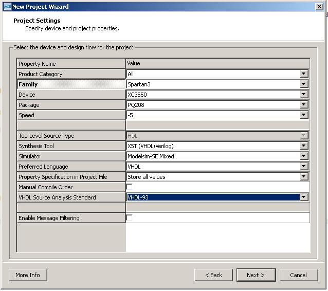
7 Click Next and specify Family : Xilinx11x Spartan3 Device : 3s50 Package : pq208 Speed Grade : -4 Simulator : ModelSim SE VHDL or ModelSim SE mixed 7
8 8

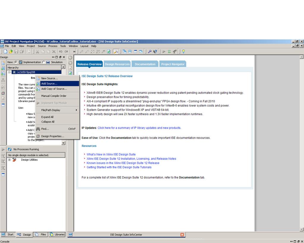
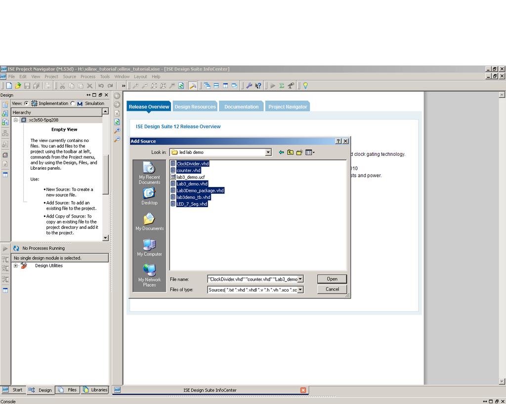
9 Click Finish and then Add Source. Choose files for the project. 9
10 10
11 11

12 Then click Ok. Your project has been defined. 12

13 2. Behavioral simulation In the Design Menu we choose Behavioral Simulation. The testbench for this design was set as a top level. In the Processes menu choose ModelSim Simulator, Simulate Behavioral Model, right-click and choose Run. 13

14 You will see a picture similar to the one above. 14
15 Finally, you should be able to observe waveforms for your design. 15
16 3. Pin Assignment Go to menu Sources for and change this option to Synthesis/Implementation. Click on Assign Package Pins. The User Constraint File (UCF) will be created if you decide to assign design port names to the physical pins. Columns I/O Names and I/O Descriptions represent ports from your design. The Loc column should be used to input the location of the corresponding pin in the FPGA device. 16
17 17
.")
18 We can specify Pin Assignments by going to User Constraint menu. We can assign design port names to the physical pins of a chosen device by option Edit Constraints (Text). Keyword NET is for a port name assignment and keyword LOC is for a physical pin assignment. 18
19 4. Synthesis and Implementation 4.1 Synthesis with Xilinx XST Go to the menu Sources for and change this option to Synthesis/Implementation. Click Check Syntax to check if vhdl sources are properly coded. 19
20 When you right-click on Generate Post-Synthesis Simulation Model then pop-up menu appears. ChooseRun to start synthesis (There is no option to simulate post-synthesis netlist for Xilinx ISE WebPack). But you can see the post synthesis vhdl file in folder <project name>- <netgen> <synthesis> 20
21 When Synthesis process is completed, the report from synthesis becomes available. Some of the most important features of the design are the minimum clock period and the maximum clock frequency. We can find these two parameters in the report file from Synthesis. Please remember that the values of these parameters after synthesis are different than the values of the same parameters after implementation. The other important information we can find in this report is the amount of FPGA resources your design requires. 21

22 Synthesis and generation of Post-Synthesis Simulation Model were completed successfully and we can start Implementation part. 22
23 Implementation : 23
24 4.2 Translate The first step in the Xilinx Design Flow for implementation is Translate. Under Implement Design option, choose Translate, and then Run. If you are successful with this part you should generate Post Translate Simulation Model. 4.3 Post-Translate Simulation When you right-click on Generate Post-Translate Simulation Model then pop-up menu appears. Choose Run to start. In the menu Sources for we choose Post-Translate Simulation. The testbench for this design was set as a top level. In the menu Processes for choose ModelSim Simulator, right-click and choose Run. ModelSim SE will be launched and waveforms for our design should appear. We can save script for further re-simulation by saving.do type files. 24
25 There is in the bottom part ModelSim terminal. We can type there commands such like do name_of_script.do and our waveform will be updated. It is possible to use terminal in every step of implementation. 4.4 Map Go to the menu Sources for and change this option to Synthesis/Implementation. From the Implement Design menu choose Map. Do right-click and pop-up menu should appear. Choose Run to start mapping process. Post-Map Simulation When you right-click on Generate Post-Map Simulation Model then pop-up menu appears. Choose Run to start. In the menu Sources for we choose Post-Map Simulation. The testbench for this design was set as a top level. In the menu Processes for choose ModelSim Simulator, right-click and choose Run. 25
26 4.5 Place and Route Go to menu Sources for and change this option to Synthesis/Implementation. From the Implement Design menu choose Place and Route. Do right-click and pop-up menu should appear. Choose Run to start place and route process. When we right-click on Generate Post Place and Route Simulation Model then pop-up menu appears and you should choose Run. 26
27 4.6 Post Place and Route Simulation In the menu Sources for we choose Post-Route Simulation. The testbench for this design was set as a top level. In the menu Processes for choose ModelSim Simulator, right-click and choose Run. ModelSim SE will be launched and waveforms for our design should appear. 27

28 4.7 Implementation Reports Review the Implementation Reports shown in the following pages. 28
29 29
30 30
31 . 31

32 4.8 Bit Stream Generation Go to menu Sources for and change this option to Synthesis/Implementation. Choose Generate Programming File, do right-click and pop-up menu should appear. Choose Run to start bit generation process. 32

33 4. Uploading Bitstream to FPGA Board Before uploading Bit file, make sure that you change your constant values in all your files to proper values, and re-synthesize/re-implement all the files. In particular, in our example, please change the value of the constant slow_clock_period in the Lab3Demo_package.vhd. Select the Adept program as shown in the picture above. When the program is opened, a device will be shown if it is connected and recognized. Select the bit file by clicking Browse and finding the appropriate file. Click Program to program the file device. 33

34 Good luck! Have fun debugging =) 34
Tutorial on FPGA Design Flow based on Xilinx ISE Webpack and ModelSim. ver. 1.3
 Tutorial on FPGA Design Flow based on Xilinx ISE Webpack and ModelSim ver. 1.3 1 Prepared by Marcin Rogawski, Ekawat (Ice) Homsirikamol, Kishorekum Surapathi, and Dr. Kris Gaj The example codes used in
Tutorial on FPGA Design Flow based on Aldec Active HDL. Ver 1.5
 Tutorial on FPGA Design Flow based on Aldec Active HDL Ver 1.5 1 Prepared by Ekawat (Ice) Homsirikamol, Marcin Rogawski, Jeremy Kelly, Kishore Kumar Surapathi and Dr. Kris Gaj This tutorial assumes that
Tutorial on FPGA Design Flow based on Xilinx ISE WebPack and ModelSim. ver. 2.0
 Tutorial on FPGA Design Flow based on Xilinx ISE WebPack and ModelSim ver. 2.0 Updated: Fall 2013 1 Preparing the Input: Download examples associated with this tutorial posted at http://ece.gmu.edu/tutorials-and-lab-manuals
Tutorial on FPGA Design Flow based on Xilinx ISE Webpack andisim. ver. 1.0
 Tutorial on FPGA Design Flow based on Xilinx ISE Webpack andisim ver. 1.0 1 Prepared by Malik Umar Sharif and Dr. Kris Gaj The example codes used in this tutorial can be obtained from http://ece.gmu.edu/coursewebpages/ece/ece448/s11/labs/448_lab3.htm
Tutorial on FPGA Design Flow based on Aldec Active HDL. ver 1.6
 Tutorial on FPGA Design Flow based on Aldec Active HDL ver 1.6 Fall 2011 1 Prepared by Ekawat (Ice) Homsirikamol, Marcin Rogawski, Jeremy Kelly, Kishore Kumar Surapathi, Ambarish Vyas, Umar Sharif and
Tutorial on FPGA Design Flow based on Aldec Active HDL. ver 1.7
 Tutorial on FPGA Design Flow based on Aldec Active HDL ver 1.7 Fall 2012 1 Prepared by Ekawat (Ice) Homsirikamol, Marcin Rogawski, Jeremy Kelly, Kishore Kumar Surapathi, Ambarish Vyas, Malik Umar Sharif
Tutorial on FPGA Design Flow based on Aldec Active HDL. Ver 1.5
 Tutorial on FPGA Design Flow based on Aldec Active HDL Ver 1.5 1 Prepared by Ekawat (Ice) Homsirikamol, Marcin Rogawski, Jeremy Kelly, John Pham, and Dr. Kris Gaj This tutorial assumes that you have basic
ELEC 204 Digital System Design LABORATORY MANUAL
 ELEC 204 Digital System Design LABORATORY MANUAL : Introductory Tutorial For Xilinx ISE Foundation v10.1 & Implementing XOR Gate College of Engineering Koç University Important Note: In order to effectively
Programming Xilinx SPARTAN 3 Board (Simulation through Implementation)
") Programming Xilinx SPARTAN 3 Board (Simulation through Implementation) September 2008 Prepared by: Oluwayomi Adamo Class: Project IV University of North Texas FPGA Physical Description 4 1. VGA (HD-15)
Programming Xilinx SPARTAN 3 Board (Simulation through Implementation) September 2008 Prepared by: Oluwayomi Adamo Class: Project IV University of North Texas FPGA Physical Description 4 1. VGA (HD-15)
Nexys 2/3 board tutorial (Decoder, ISE 13.2) Jim Duckworth, August 2011, WPI. (updated March 2012 to include Nexys2 board)
 Jim Duckworth, August 2011, WPI. (updated March 2012 to include Nexys2 board)") Nexys 2/3 board tutorial (Decoder, ISE 13.2) Jim Duckworth, August 2011, WPI. (updated March 2012 to include Nexys2 board) Note: you will need the Xilinx ISE Webpack installed on your computer (or you
Nexys 2/3 board tutorial (Decoder, ISE 13.2) Jim Duckworth, August 2011, WPI. (updated March 2012 to include Nexys2 board) Note: you will need the Xilinx ISE Webpack installed on your computer (or you
Xilinx ISE Synthesis Tutorial
 Xilinx ISE Synthesis Tutorial The following tutorial provides a basic description of how to use Xilinx ISE to create a simple 2-input AND gate and synthesize the design onto the Spartan-3E Starter Board
Nexys 2 board tutorial (Decoder, ISE 12.2) Jim Duckworth, August 2010, WPI. Digilent Adept Programming Steps added by Zoe (Zhu Fu)
 Jim Duckworth, August 2010, WPI. Digilent Adept Programming Steps added by Zoe (Zhu Fu)") Nexys 2 board tutorial (Decoder, ISE 12.2) Jim Duckworth, August 2010, WPI. Digilent Adept Programming Steps added by Zoe (Zhu Fu) Note: you will need the Xlinx ISE Webpack installed on your compuer (or
Nexys 2 board tutorial (Decoder, ISE 12.2) Jim Duckworth, August 2010, WPI. Digilent Adept Programming Steps added by Zoe (Zhu Fu) Note: you will need the Xlinx ISE Webpack installed on your compuer (or
Laboratory #Intro to Xilinx ISE and CR-2 Kit ECE 332
 Name: G Number: 1 Introduction Laboratory #Intro to Xilinx ISE and CR-2 Kit ECE 332 The purpose of this laboratory is to introduce the design tools used in ECE 332 lab. In this lab you will learn about
Circuit design with configurable devices (FPGA)
") 1 Material Circuit design with configurable devices (FPGA) Computer with Xilinx's ISE software installed. Digilent's Basys2 prototype board and documentation. Sample design files (lab kit). Files and documents
1 Material Circuit design with configurable devices (FPGA) Computer with Xilinx's ISE software installed. Digilent's Basys2 prototype board and documentation. Sample design files (lab kit). Files and documents
EE 367 Logic Design Lab #1 Introduction to Xilinx ISE and the ML40X Eval Board Date: 1/21/09 Due: 1/28/09
 EE 367 Logic Design Lab #1 Introduction to Xilinx ISE and the ML40X Eval Board Date: 1/21/09 Due: 1/28/09 Lab Description Today s lab will introduce you to the Xilinx Integrated Software Environment (ISE)
Tutorial: Working with Verilog and the Xilinx FPGA in ISE 9.2i
 Tutorial: Working with Verilog and the Xilinx FPGA in ISE 9.2i This tutorial will show you how to: Use Verilog to specify a design Simulate that Verilog design Define pin constraints for the FPGA (.ucf
TLL5000 Electronic System Design Base Module. Getting Started Guide, Ver 3.4
 TLL5000 Electronic System Design Base Module Getting Started Guide, Ver 3.4 COPYRIGHT NOTICE The Learning Labs, Inc. ( TLL ) All rights reserved, 2008 Reproduction in any form without permission is prohibited.
TLL5000 Electronic System Design Base Module
 TLL5000 Electronic System Design Base Module The Learning Labs, Inc. Copyright 2007 Manual Revision 2007.12.28 1 Copyright 2007 The Learning Labs, Inc. Copyright Notice The Learning Labs, Inc. ( TLL )
Xilinx Project Navigator Reference Guide
 31 July 2003 Author: David M. Sendek Xilinx Project Navigator Reference Guide Background: This guide provides you with step-by-step procedures in using the Xilinx Project Navigator to perform the following:
Xilinx ISE8.1 and Spartan-3 Tutorial EE3810
 Xilinx ISE8.1 and Spartan-3 Tutorial EE3810 1 Part1) Starting a new project Simple 3-to-8 Decoder Start the Xilinx ISE 8.1i Project Navigator: Select File > New Project in the opened window 2 Select a
ECE 4305 Computer Architecture Lab #1
 ECE 4305 Computer Architecture Lab #1 The objective of this lab is for students to familiarize with the FPGA prototyping system board (Nexys-2) and the Xilinx software development environment that will
Verilog Design Entry, Synthesis, and Behavioral Simulation
 ------------------------------------------------------------- PURPOSE - This lab will present a brief overview of a typical design flow and then will start to walk you through some typical tasks and familiarize
AccelDSP tutorial 2 (Matlab.m to HDL for Xilinx) Ronak Gandhi Syracuse University Fall
 Ronak Gandhi Syracuse University Fall") AccelDSP tutorial 2 (Matlab.m to HDL for Xilinx) Ronak Gandhi Syracuse University Fall 2009-10 AccelDSP Getting Started Tutorial Introduction This tutorial exercise will guide you through the process of
AccelDSP tutorial 2 (Matlab.m to HDL for Xilinx) Ronak Gandhi Syracuse University Fall 2009-10 AccelDSP Getting Started Tutorial Introduction This tutorial exercise will guide you through the process of
CCE 3202 Advanced Digital System Design
 CCE 3202 Advanced Digital System Design Lab Exercise #2 Introduction You will use Xilinx Webpack v9.1 to allow the synthesis and creation of VHDLbased designs. This lab will outline the steps necessary
Revision: February 27, E Main Suite D Pullman, WA (509) Voice and Fax
 Voice and Fax") Xilinx ISE WebPACK VHDL Tutorial Revision: February 27, 2010 215 E Main Suite D Pullman, WA 99163 (509) 334 6306 Voice and Fax Overview This tutorial provides simple instruction for using the Xilinx ISE
Xilinx ISE WebPACK VHDL Tutorial Revision: February 27, 2010 215 E Main Suite D Pullman, WA 99163 (509) 334 6306 Voice and Fax Overview This tutorial provides simple instruction for using the Xilinx ISE
Building Combinatorial Circuit Using Behavioral Modeling Lab
 Building Combinatorial Circuit Using Behavioral Modeling Lab Overview: In this lab you will learn how to model a combinatorial circuit using behavioral modeling style of Verilog HDL. You will model a combinatorial
EE 1315 DIGITAL LOGIC LAB EE Dept, UMD
 EE 1315 DIGITAL LOGIC LAB EE Dept, UMD EXPERIMENT # 1: Logic building blocks The main objective of this experiment is to let you familiarize with the lab equipment and learn about the operation of the
Tutorial: ISE 12.2 and the Spartan3e Board v August 2010
 Tutorial: ISE 12.2 and the Spartan3e Board v12.2.1 August 2010 This tutorial will show you how to: Use a combination of schematics and Verilog to specify a design Simulate that design Define pin constraints
4. Verify that HDL is selected as the Top-Level Source Type, and click Next. The New Project Wizard Device Properties page appears.
 Working with the GODIL Author: Ruud Baltissen Credits: Michael Randelzhofer, Ed Spittles Date: August 2010 What is it? This document describes a way to get familiar with the Xilinx FPGAs on OHO s Godil,
Xilinx ChipScope ICON/VIO/ILA Tutorial
 Xilinx ChipScope ICON/VIO/ILA Tutorial The Xilinx ChipScope tools package has several modules that you can add to your Verilog design to capture input and output directly from the FPGA hardware. These
ECT 224: Digital Computer Fundamentals Using Xilinx StateCAD
 ECT 224: Digital Computer Fundamentals Using Xilinx StateCAD 1) Sequential circuit design often starts with a problem statement tat can be realized in the form of a state diagram or state table a) Xilinx
Graduate Institute of Electronics Engineering, NTU. FPGA Lab. Speaker : 鍾明翰 (CMH) Advisor: Prof. An-Yeu Wu Date: 2010/12/14 ACCESS IC LAB
 Advisor: Prof. An-Yeu Wu Date: 2010/12/14 ACCESS IC LAB") FPGA Lab Speaker : 鍾明翰 (CMH) Advisor: Prof. An-Yeu Wu Date: 2010/12/14 ACCESS IC LAB Objective In this Lab, you will learn the basic set-up and design methods of implementing your design by ISE 10.1. Create
FPGA Lab Speaker : 鍾明翰 (CMH) Advisor: Prof. An-Yeu Wu Date: 2010/12/14 ACCESS IC LAB Objective In this Lab, you will learn the basic set-up and design methods of implementing your design by ISE 10.1. Create
FPGA Design Tutorial
 ECE 554 Digital Engineering Laboratory FPGA Design Tutorial Version 5.0 Fall 2006 Updated Tutorial: Jake Adriaens Original Tutorial: Matt King, Surin Kittitornkun and Charles R. Kime Table of Contents
Timing Analysis in Xilinx ISE
 Timing Analysis in Xilinx ISE For each design which is to be implemented, constraints should be defined to get predictable results. The first important class of constraints was already introduced in the
Circuit Design and Simulation with VHDL 2nd edition Volnei A. Pedroni MIT Press, 2010 Book web:
 Circuit Design and Simulation with VHDL 2nd edition Volnei A. Pedroni MIT Press, 2010 Book web: www.vhdl.us Appendix C Xilinx ISE Tutorial (ISE 11.1) This tutorial is based on ISE 11.1 WebPack (free at
Laboratory of Digital Circuits Design: Design, Implementation and Simulation of Digital Circuits Using Programmable Devices
 Internet Engineering Dr. Jarosław Sugier Laboratory of Digital Circuits Design: Design, Implementation and Simulation of Digital Circuits Using Programmable Devices This document presents software packages
Design a three-input, two-output sequential digital circuit which functions as a digital locking mechanism. LOCK ALARM
 Department of Computing Course 112 Hardware First Year Laboratory Assignment Dates for the session 2005-2006: Hand out Date: 10 th January 2006 Hand in deadline (electronic and written report): 17.00 Monday
Board-Data Processing. VHDL Exercises. Exercise 1: Basics of VHDL Programming. Stages of the Development process using FPGA s in Xilinx ISE.
 Board-Data Processing VHDL Exercises Exercise 1: Basics of VHDL Programming Stages of the Development process using FPGA s in Xilinx ISE. Basics of VHDL VHDL (Very High Speed IC Hardware description Language)
Logic Implementation on a Xilinx FPGA using VHDL WWU Linux platform assumed. rev 10/25/16
 1 Logic Implementation on a Xilinx FPGA using VHDL WWU Linux platform assumed. rev 10/25/16 The following is a general outline of steps (i.e. design flow) used to implement a digital system described with
Getting Started with Xilinx WebPack 13.1
 Getting Started with Xilinx WebPack 13.1 B. Ackland June 2011 (Adapted from S. Tewksbury notes WebPack 7.1) This tutorial is designed to help you to become familiar with the operation of the WebPack software
Using Synplify Pro, ISE and ModelSim
 Using Synplify Pro, ISE and ModelSim VLSI Systems on Chip ET4 351 Rene van Leuken Huib Lincklaen Arriëns Rev. 1.2 The EDA programs that will be used are: For RTL synthesis: Synplicity Synplify Pro For
Revision: February 27, E Main Suite D Pullman, WA (509) Voice and Fax
 Voice and Fax") Xilinx ISE WebPACK Schematic Capture Tutorial Revision: February 27, 2010 215 E Main Suite D Pullman, WA 99163 (509) 334 6306 Voice and Fax Overview This tutorial provides instruction for using the Xilinx
Xilinx ISE WebPACK Schematic Capture Tutorial Revision: February 27, 2010 215 E Main Suite D Pullman, WA 99163 (509) 334 6306 Voice and Fax Overview This tutorial provides instruction for using the Xilinx
Xilinx ISE8.1 and Spartan-3 Tutorial (Prepared by Kahraman Akdemir based on Professor Duckworth's Tutorials updated September 2006)
") Xilinx ISE8.1 and Spartan-3 Tutorial (Prepared by Kahraman Akdemir based on Professor Duckworth's Tutorials updated September 2006) 1 Part1) Starting a new project Simple 3-to-8 Decoder Start the Xilinx
Xilinx ISE8.1 and Spartan-3 Tutorial (Prepared by Kahraman Akdemir based on Professor Duckworth's Tutorials updated September 2006) 1 Part1) Starting a new project Simple 3-to-8 Decoder Start the Xilinx
Xilinx Tutorial Basic Walk-through
 Introduction to Digital Logic Design with FPGA s: Digital logic circuits form the basis of all digital electronic devices. FPGAs (Field Programmable Gate Array) are large programmable digital electronic
Logic Implementation on a Xilinx FPGA using VHDL WWU Linux platform assumed. rev 11/01/17
 1 Logic Implementation on a Xilinx FPGA using VHDL WWU Linux platform assumed. rev 11/01/17 The following is a general outline of steps (i.e. design flow) used to implement a digital system described with
ECE 491 Laboratory 1 Introducing FPGA Design with Verilog September 6, 2004
 Goals ECE 491 Laboratory 1 Introducing FPGA Design with Verilog September 6, 2004 1. To review the use of Verilog for combinational logic design. 2. To become familiar with using the Xilinx ISE software
DIGITAL LOGIC WITH VHDL (Fall 2013) Unit 1
 Unit 1") DIGITAL LOGIC WITH VHDL (Fall 23) Unit DESIGN FLOW DATA TYPES LOGIC GATES WITH VHDL TESTBENCH GENERATION DESIGN FLOW Design Entry: We specify the logic circuit using a Hardware Description Language (e.g.,
DIGITAL LOGIC WITH VHDL (Fall 23) Unit DESIGN FLOW DATA TYPES LOGIC GATES WITH VHDL TESTBENCH GENERATION DESIGN FLOW Design Entry: We specify the logic circuit using a Hardware Description Language (e.g.,
Lab 3 Sequential Logic for Synthesis. FPGA Design Flow.
 Lab 3 Sequential Logic for Synthesis. FPGA Design Flow. Task 1 Part 1 Develop a VHDL description of a Debouncer specified below. The following diagram shows the interface of the Debouncer. The following
COS/ELE 375 Verilog & Design Tools Tutorial
 COS/ELE 375 Verilog & Design Tools Tutorial In this tutorial, you will walk through a tutorial using the Xilinx ISE design software with a Digilent Nexys4 DDR FPGA board. In this tutorial, you will learn
LABORATORY # 6 * L A B M A N U A L. Datapath Components - Adders
 Department of Electrical Engineering University of California Riverside Laboratory #6 EE 120 A LABORATORY # 6 * L A B M A N U A L Datapath Components - Adders * EE and CE students must attempt also to
ELEC 4200 Lab#0 Tutorial
 1 ELEC 4200 Lab#0 Tutorial Objectives(1) In this Lab exercise, we will design and implement a 2-to-1 multiplexer (MUX), using Xilinx Vivado tools to create a VHDL model of the design, verify the model,
Using the ChipScope Pro for Testing HDL Designs on FPGAs
 Using the ChipScope Pro for Testing HDL Designs on FPGAs Compiled by OmkarCK CAD Lab, Dept of E&ECE, IIT Kharagpur. Introduction: Simulation based method is widely used for debugging the FPGA design on
PlanAhead Release Notes
 PlanAhead Release Notes What s New in the 11.1 Release UG656(v 11.1.0) April 27, 2009 PlanAhead 11.1 Release Notes Page 1 Table of Contents What s New in the PlanAhead 11.1 Release... 4 Device Support...
and 32 bit for 32 bit. If you don t pay attention to this, there will be unexpected behavior in the ISE software and thing may not work properly!
 This tutorial will show you how to: Part I: Set up a new project in ISE 14.7 Part II: Implement a function using Schematics Part III: Simulate the schematic circuit using ISim Part IV: Constraint, Synthesize,
Getting started with the Xilinx Project Navigator and the Digilent BASYS 2 board.
 Getting started with the Xilinx Project Navigator and the Digilent BASYS 2 board. This lab is based on: Xilinx Project Navigator, Release Version 14.6 Digilent Adept System Rev 2.7, Runtime Rev 2.16 Digilent
ISE Design Suite Software Manuals and Help
 ISE Design Suite Software Manuals and Help These documents support the Xilinx ISE Design Suite. Click a document title on the left to view a document, or click a design step in the following figure to
Xilinx Schematic Entry Tutorial
 Overview Xilinx Schematic Entry Tutorial Xilinx ISE Schematic Entry & Modelsim Simulation What is circuit simulation and why is it important? Complex designs, short design cycle Simultaneous system design
Quick Front-to-Back Overview Tutorial
 Quick Front-to-Back Overview Tutorial PlanAhead Design Tool This tutorial document was last validated using the following software version: ISE Design Suite 14.5 If using a later software version, there
Digital Circuit Design Using Xilinx ISE Tools
 Digital Circuit Design Using Xilinx ISE Tools Poras T. Balsara and Prashant Vallur Table of Contents 1. Introduction 2. Programmable logic devices: FPGA and CPLD 3. Creating a new project in Xilinx Foundation
Tutorial: Working with the Xilinx tools 14.4
 Tutorial: Working with the Xilinx tools 14.4 This tutorial will show you how to: Part I: Set up a new project in ISE Part II: Implement a function using Schematics Part III: Implement a function using
Tutorial - Using Xilinx System Generator 14.6 for Co-Simulation on Digilent NEXYS3 (Spartan-6) Board
 Board") Tutorial - Using Xilinx System Generator 14.6 for Co-Simulation on Digilent NEXYS3 (Spartan-6) Board Shawki Areibi August 15, 2017 1 Introduction Xilinx System Generator provides a set of Simulink blocks
Tutorial - Using Xilinx System Generator 14.6 for Co-Simulation on Digilent NEXYS3 (Spartan-6) Board Shawki Areibi August 15, 2017 1 Introduction Xilinx System Generator provides a set of Simulink blocks
Xilinx ISE/WebPack: Introduction to Schematic Capture and Simulation
 Xilinx ISE/WebPack: Introduction to Schematic Capture and Simulation Revision: February 7, 2003 Overview This document is intended to assist new entry-level users of the Xilinx ISE/WebPack software. It
Introduction to WebPACK 8.1. Using Xilinx WebPACK Software to Create FPGA Designs for the XSA Board
 Introduction to WebPACK 8.1 Using Xilinx WebPACK Software to Create FPGA Designs for the XSA Board Release date: 5/16/2005 2006 by XESS Corp. All XS-prefix product designations are trademarks of XESS
MANUAL XILINX ISE PROJECT NAVIGATOR
 Hochschule für Angewandte Wissenschaften Hamburg University of Applied Sciences Department of Electrical Engineering and Computer Sciences MANUAL XILINX ISE PROJECT NAVIGATOR AND MODELSIM Design Flow for
Introduction. In this exercise you will:
 Introduction In a lot of digital designs (DAQ, Trigger,..) the FPGAs are used. The aim of this exercise is to show you a way to logic design in a FPGA. You will learn all the steps from the idea to the
CPLD Experiment 4. XOR and XNOR Gates with Applications
 CPLD Experiment 4 XOR and XNOR Gates with Applications Based on Xilinx ISE Design Suit 10.1 Department of Electrical & Computer Engineering Florida International University Objectives Materials Examining
CSE 591: Advanced Hardware Design and Verification (2012 Spring) LAB #0
 LAB #0") Lab 0: Tutorial on Xilinx Project Navigator & ALDEC s Active-HDL Simulator CSE 591: Advanced Hardware Design and Verification Assigned: 01/05/2011 Due: 01/19/2011 Table of Contents 1 Overview... 2 1.1
Lab 0: Tutorial on Xilinx Project Navigator & ALDEC s Active-HDL Simulator CSE 591: Advanced Hardware Design and Verification Assigned: 01/05/2011 Due: 01/19/2011 Table of Contents 1 Overview... 2 1.1
The board is powered by the USB connection, so to turn it on or off you plug it in or unplug it, respectively.
 Lab 1 You may work in pairs or individually on this lab Lab Objectives Learn about the equipment we will be using and how to handle it safely. Learn the basics of using Xilinx ISE to develop hardware designs
Implementing a Verilog design into the UWEE CPLD Development Board Using Xilinx s ISE 7.1i Software: A Tutorial
 Implementing a Verilog design into the UWEE CPLD Development Board Using Xilinx s ISE 7.1i Software: A Tutorial Revision 0 By: Evan Gander Materials: The following are required in order to complete this
Introduction to WebPACK 3.1. Using XILINX WebPACK Software to Create CPLD Designs
 Introduction to WebPACK 3.1 Using XILINX WebPACK Software to Create CPLD Designs RELEASE DATE: 8/28/2000 All XS-prefix product designations are trademarks of XESS Corp. All XC-prefix product designations
1. Downloading. 2. Installation and License Acquiring. Xilinx ISE Webpack + Project Setup Instructions
 Xilinx ISE Webpack + Project Setup Instructions 1. Downloading The Xilinx tools are free for download from their website and can be installed on your Windowsbased PC s. Go to the following URL: http://www.xilinx.com/support/download/index.htm
OVERVIEW OF FPGA AND EDA SOFTWARE
 CHAPTER 2 OVERVIEW OF FPGA AND EDA SOFTWARE 2.1 INTRODUCTION Developing a large FPGA-based system is an involved process that consists of many complex transformations and optimization algorithms. Software
Introduction to Xilinx Vivado tools
 Introduction to Xilinx Vivado tools This document is meant to be a starting point for users who are new to using the Xilinx Vivado tools. The document will describe the basic steps to start, create, simulate,
Lab 3 Finite State Machines Movie Ticket Dispensing Machine
 Lab 3 Finite State Machines Movie Ticket Dispensing Machine Design, implement, verify, and test a Movie Ticket Dispensing Machine based on the following specification: The machine should allow the choice
MicroBlaze Tutorial on EDK 10.1 using Sparatan III E Behavioural Simulation of MicroBlaze System
 MicroBlaze Tutorial on EDK 10.1 using Sparatan III E Behavioural Simulation of MicroBlaze System Ahmed Elhossini January 24, 2010 1 Introduction 1.1 Objectives This tutorial will demonstrate process of
Spartan-6 LX9 MicroBoard Embedded Tutorial. Tutorial 1 Creating an AXI-based Embedded System
 Spartan-6 LX9 MicroBoard Embedded Tutorial Tutorial 1 Creating an AXI-based Embedded System Version 13.1.01 Revision History Version Description Date 13.1.01 Initial release for EDK 13.1 5/15/2011 Table
Installation Guide for Digital Hardware Design Entry and Verification Tools (Prepared by: Yogesh Varna, Hardware Design Trainer)
") Computer Hardware Design (ECE 4623/5623 by Dr. Monte Tull) Installation Guide for Digital Hardware Design Entry and Verification Tools (Prepared by: Yogesh Varna, Hardware Design Trainer) The design assignments
Computer Hardware Design (ECE 4623/5623 by Dr. Monte Tull) Installation Guide for Digital Hardware Design Entry and Verification Tools (Prepared by: Yogesh Varna, Hardware Design Trainer) The design assignments
Vivado Walkthrough ECGR Fall 2015
 ECGR 2181 - Vivado Walkthrough 1 Vivado Walkthrough ECGR 2181 - Fall 2015 Intro In this walkthrough we re going to go through the process of creating a project, adding sources, writing vhdl, simulating
SDRAM Interface Clocking for the NanoBoard 2
 SDRAM Interface Clocking for the NanoBoard 2 NB2 + DB30 Xilinx Spartan 3 DaughterBoard 1. Schematic wiring for Xilinx DCM clocks. 2. Shared Memory Port Plugin wiring. NB2 + DB31 Altera Cyclone II DaughterBoard
XILINX ISE AND SPARTAN 3AN TUTORIAL
 XILINX ISE AND SPARTAN 3AN TUTORIAL SYNTETIZE AND SIMULATION------------------------------------------ This tutorial will show you how to create a simple Xilinx ISE project based on the Spartan-3 Board.
Introduction to WebPACK 6.3. Using Xilinx WebPACK Software to Create FPGA Designs for the XSA Board
 Introduction to WebPACK 6.3 Using Xilinx WebPACK Software to Create FPGA Designs for the XSA Board Release date: 1/1/2005 2005 by XESS Corp. All XS-prefix product designations are trademarks of XESS Corp.
Creating the AVS6LX9MBHP211 MicroBlaze Hardware Platform for the Spartan-6 LX9 MicroBoard Version
 Creating the AVS6LX9MBHP211 MicroBlaze Hardware Platform for the Spartan-6 LX9 MicroBoard Version 13.2.01 Revision History Version Description Date 12.4.01 Initial release for EDK 12.4 09 Mar 2011 12.4.02
University of Hawaii EE 361L. Getting Started with Spartan 3E Digilent Basys2 Board. Lab 4.1
 University of Hawaii EE 361L Getting Started with Spartan 3E Digilent Basys2 Board Lab 4.1 I. Test Basys2 Board Attach the Basys2 board to the PC or laptop with the USB connector. Make sure the blue jumper
Steps to run compxlib to compile Xilinx libraries in Modelsim SE 10.1 for EE101/EE201L/EE560 students as well as USC ITS
 Gandhi Puvvada Steps to run compxlib to compile Xilinx libraries in Modelsim SE 10.1 for EE101/EE201L/EE560 students as well as USC ITS 1 Finish installing Xilinx ISE 13.2 and ModelSim SE 10.1 1.1 We assume
Introduction to WebPACK 4.1 for CPLDs. Using Xilinx WebPACK Software to Create CPLD Designs for the XS95 Board
 Introduction to WebPACK 4.1 for CPLDs Using Xilinx WebPACK Software to Create CPLD Designs for the XS95 Board Release date: 10/29/2001 All XS-prefix product designations are trademarks of XESS Corp. All
Introduction to WebPACK 5.2 for FPGAs. Using Xilinx WebPACK Software to Create FPGA Designs for the XSB-300E Board
 Introduction to WebPACK 5.2 for FPGAs Using Xilinx WebPACK Software to Create FPGA Designs for the XSB-300E Board Release date: 10/27/2003 All XS-prefix product designations are trademarks of XESS Corp.
CS152 FPGA CAD Tool Flow University of California at Berkeley College of Engineering Department of Electrical Engineering and Computer Sciences
 CS152 FPGA CAD Tool Flow University of California at Berkeley College of Engineering Department of Electrical Engineering and Computer Sciences Compiled: 4/3/2003 for CS152 Spring 03, Prof. John Kubiatowicz
EE183 LAB TUTORIAL. Introduction. Projects. Design Entry
 EE183 LAB TUTORIAL Introduction You will be using several CAD tools to implement your designs in EE183. The purpose of this lab tutorial is to introduce you to the tools that you will be using, Xilinx
Commas and Data Alignment Lab
 Lab Workbook Introduction In this lab, you will use commas to control data flow and align serial data into bytes. Objectives After completing this lab, you will be able to: Procedure Define a data alignment
!"#$%&'()*+%&,-%&.*/.&0"&#%(1.*"0* 2+345*!%(,',%6.7*87'()*9/:37* :."&).*A%7"(*8('B.&7'6=* 8C2C3C*
*+%&,-%&.*/.&0&#%(1.*0* 2+345*!%(,',%6.7*87'()*9/:37* :.&).*A%7(*8('B.&7'6=* 8C2C3C*") !"#$%&'()*+%&,-%&.*/.&0"&#%(1.*"0* 2+345*!%(,',%6.7*87'()*9/:37* ;&
!"#$%&'()*+%&,-%&.*/.&0"&#%(1.*"0* 2+345*!%(,',%6.7*87'()*9/:37* ;&
Introduction to WebPACK 4.1 for FPGAs. Using Xilinx WebPACK Software to Create FPGA Designs for the XSA Board
 Introduction to WebPACK 4.1 for FPGAs Using Xilinx WebPACK Software to Create FPGA Designs for the XSA Board Release date: 10/29/2001 All XS-prefix product designations are trademarks of XESS Corp. All
Revision: February 26, E Main Suite D Pullman, WA (509) Voice and Fax
 Voice and Fax") MCS File Creation with Xilinx ISE Tutorial Revision: February 26, 2010 215 E Main Suite D Pullman, WA 99163 (509) 334 6306 Voice and Fax Overview This tutorial provides instruction for creating an.mcs
MCS File Creation with Xilinx ISE Tutorial Revision: February 26, 2010 215 E Main Suite D Pullman, WA 99163 (509) 334 6306 Voice and Fax Overview This tutorial provides instruction for creating an.mcs
FPGA Design Flow. - from HDL to physical implementation - Victor Andrei. Kirchhoff-Institut für Physik (KIP) Ruprecht-Karls-Universität Heidelberg
 Ruprecht-Karls-Universität Heidelberg") FPGA Design Flow - from HDL to physical implementation - Victor Andrei Kirchhoff-Institut für Physik (KIP) Ruprecht-Karls-Universität Heidelberg 6th Detector Workshop of the Helmholtz Alliance Physics
FPGA Design Flow - from HDL to physical implementation - Victor Andrei Kirchhoff-Institut für Physik (KIP) Ruprecht-Karls-Universität Heidelberg 6th Detector Workshop of the Helmholtz Alliance Physics
Programmable Logic Design I
 Programmable Logic Design I Introduction In labs 11 and 12 you built simple logic circuits on breadboards using TTL logic circuits on 7400 series chips. This process is simple and easy for small circuits.
Introduction. About this tutorial. How to use this tutorial
 Basic Entry & not About this tutorial This tutorial consists of an introduction to creating simple circuits on an FPGA using a variety of methods. There are two ways to create the circuit: using or by
Lab 1: Introduction to Verilog HDL and the Xilinx ISE
 EE 231-1 - Fall 2016 Lab 1: Introduction to Verilog HDL and the Xilinx ISE Introduction In this lab simple circuits will be designed by programming the field-programmable gate array (FPGA). At the end
Spartan-6 LX9 MicroBoard Embedded Tutorial. Lab 6 Creating a MicroBlaze SPI Flash Bootloader
 Spartan-6 LX9 MicroBoard Embedded Tutorial Lab 6 Creating a MicroBlaze SPI Flash Bootloader Version 13.1.01 Revision History Version Description Date 13.1.01 Initial release for EDK 13.1 5/17/11 Table
FPGA Design Flow 1. All About FPGA
 FPGA Design Flow 1 In this part of tutorial we are going to have a short intro on FPGA design flow. A simplified version of FPGA design flow is given in the flowing diagram. FPGA Design Flow 2 FPGA_Design_FLOW
Lab 6 : Introduction to Verilog
 Lab 6 : Introduction to Verilog Name: Sign the following statement: On my honor, as an Aggie, I have neither given nor received unauthorized aid on this academic work 1 Objective The main objective of
Vivado Design Suite Tutorial. Design Flows Overview
 Vivado Design Suite Tutorial Design Flows Overview Notice of Disclaimer The information disclosed to you hereunder (the "Materials") is provided solely for the selection and use of Xilinx products. To