EMTECH_3P_A_1_v4. Descripción de la placa.
|
|
|
- Kevin Weaver
- 5 years ago
- Views:
Transcription

1 EMTECH_3P_A_1_v4 Descripción de la placa. Autor Hidalgo Martin Versión 0.1 Ultima revisión Lunes, 04 de Abril de 2011
2 Contenido 1 Introducción Descripción de la placa Vista superior Vista Inferior Componentes en la placa Requerimientos Conexiones en la placa FPGA ProASIC3 Flash Family Fugas with Optional Soft ARM Support Dimensiones...10 Página 2 de 10
3 Revisiones Fecha Versión Modificaciones 0.1 Versión original Página 3 de 10
4 1 Introducción En este documento se describe las características de la placa, componentes existentes e interfaces entre ellos y el usuario. Con este documento podemos analizar el alcance y posibilidades de desarrollo utilizando a 3P_A_1_v4. Siguiendo con el propósito del proyecto original, para esta cuarta versión de la 3PA1 se realizo un nuevo mapeo de los pines libres para las FPGAs de encapsulado PQ208. Se agregaron 2 conectores más de 10 pines manteniendo la compatibilidad con los conectores originales de las versiones anteriores. Esta nueva disposición de pines permite colocar una nueva placa hija de memorias e implementar un núcleo Cortex-M3 sobre la FPGA. Página 4 de 10


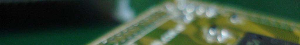
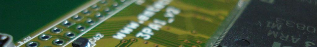
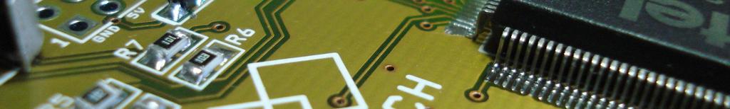
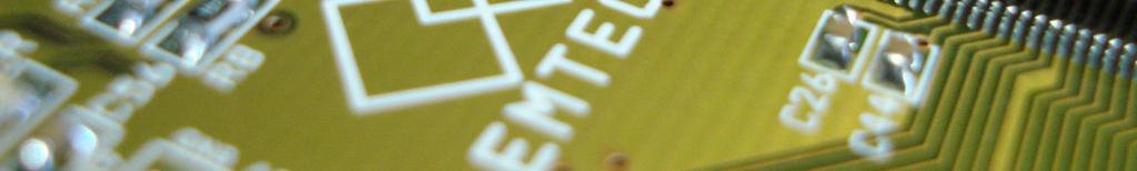
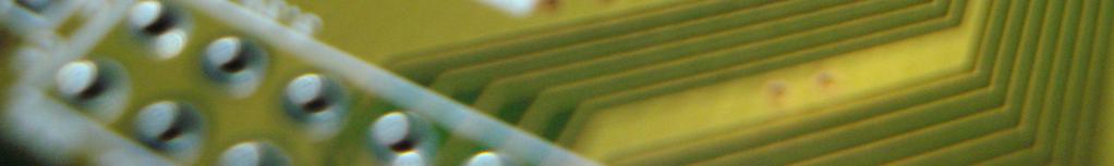
5 2 Descripción de la placa 2.1 Vista superior 2.2 Vista Inferior 1-Vista superior 2-Vista inferior Página 5 de 10

6 2.3 Componentes en la placa Dadas las posibilidades de colocar un encapsulado PQ208 o VQ100, las variables de FPGA de ACTEL que pueden soldarse en la placa son los siguientes: Power DC-DC converter 5VDC to 3.3v and 1.5v. 2.4 Requerimientos AC/DC power adapter 5VDC 2Amp 2.1mm x 5.5mm Página 6 de 10
7 2.5 Conexiones en la placa 3- esquema de conexión Página 7 de 10
8 3 FPGA ProASIC3 Flash Family Fugas with Optional Soft ARM Support Features and Benefits High Capacity 15 k to 1 M System Gates Up to 144 kbits of True Dual-Port SRAM Up to 300 User I/Os Reprogrammable Flash Technology 130-nm, 7-Layer Metal (6 Copper), Flash-Based CMOS Process Live at Power-Up (LAPU) Level 0 Support Single-Chip Solution Retains Programmed Design when Powered Off High Performance 350 MHz System Performance 3.3 V, 66 MHz 64-Bit PCI In-System Programming (ISP) and Security Secure ISP Using On-Chip 128-Bit Advanced Encryption Standard (AES) Decryption (except ARM-enabled ProASIC 3 devices) via JTAG (IEEE 1532 compliant) FlashLock to Secure FPGA Contents Low Power Core Voltage for Low Power Support for 1.5 V-Only Systems Low-Impedance Flash Switches High-Performance Routing Hierarchy Segmented, Hierarchical Routing and Clock Structure Advanced I/O 700 Mbps DDR, LVDS-Capable I/Os (A3P250 and above) 1.5 V, 1.8 V, 2.5 V, and 3.3 V Mixed-Voltage Operation Wide Range Power Supply Voltage Support per JESD8-B, Allowing I/Os to Operate from 2.7 V to 3.6 V Bank-Selectable I/O Voltages up to 4 Banks per Chip Single-Ended I/O Standards: LVTTL, LVCMOS 3.3 V / 2.5 V / 1.8 V / 1.5 V, 3.3 V PCI / 3.3 V PCI-X and LVCMOS 2.5 V / 5.0 V Input Differential I/O Standards: LVPECL, LVDS, B-LVDS, and M-LVDS (A3P250 and above) I/O Registers on Input, Output, and Enable Paths Hot-Swappable and Cold Sparing I/Os Programmable Output Slew Rate and Drive Strength Weak Pull-Up/-Down IEEE (JTAG) Boundary Scan Test Pin-Compatible Packages across the ProASIC3 Family Clock Conditioning Circuit (CCC) and PLL Six CCC Blocks, One with an Integrated PLL Configurable Phase-Shift, Multiply/Divide, Delay Capabilities and External Feedback Wide Input Frequency Range (1.5 MHz to 350 MHz) Embedded Memory 1 kbit of FlashROM User Nonvolatile Memory SRAMs and FIFOs with Variable-Aspect-Ratio 4,608-Bit RAM Blocks ( 1, 2, 4, 9, and 18 organizations) True Dual-Port SRAM (except 18) ARM Processor Support in ProASIC3 FPGAs M1 and M7 ProASIC3 Devices Cortex-M1 and CoreMP7 Soft Página 8 de 10
9 Processor Available with or without Debug General Description ProASIC3, the third-generation family of Actel flash FPGAs, offers performance, density, and features beyond those of the ProASICPLUS family. Nonvolatile flash technology gives ProASIC3 devices the advantage of being a secure, low-power, single-chip solution that is live at power-up (LAPU). ProASIC3 is reprogrammable and offers time-to-market benefits at an ASIC-level unit cost. These features enable designers to create high-density systems using existing ASIC or FPGA design flows and tools. ProASIC3 devices offer 1 kbit of on-chip, reprogrammable, nonvolatile FlashROM storage as well as clock conditioning circuitry based on an integrated phase-locked loop (PLL). The A3P015 and A3P030 devices have no PLL or RAM support. ProASIC3 devices have up to 1 million system gates, supported with up to 144 kbits of true dual-port SRAM and up to 300 user I/Os. ProASIC3 devices support the ARM7 soft IP core and Cortex-M1 devices. The ARM-enabled devices have Actel ordering numbers that begin with M7A3P (CoreMP7) and M1A3P (Cortex-M1) and do not support AES decryption. Página 9 de 10

10 4 Dimensiones Página 10 de 10
Military Grade SmartFusion Customizable System-on-Chip (csoc)
") Military Grade SmartFusion Customizable System-on-Chip (csoc) Product Benefits 100% Military Temperature Tested and Qualified from 55 C to 125 C Not Susceptible to Neutron-Induced Configuration Loss Microcontroller
Military Grade SmartFusion Customizable System-on-Chip (csoc) Product Benefits 100% Military Temperature Tested and Qualified from 55 C to 125 C Not Susceptible to Neutron-Induced Configuration Loss Microcontroller
Radiation-Tolerant ProASIC3 Low-Power Space- Flight Flash FPGAs
 Advance v0.2 Radiation-Tolerant ProASIC3 Low-Power Space- Flight Flash FPGAs with Flash*Freeze Technology Features and Benefits MIL-STD-883 Class B Qualified Packaging Ceramic Column Grid Array with Six
ProASIC 3 Flash Family FPGAs with Optional Soft ARM Support
 Advanced v0.6 ProASIC 3 Flash Family FPGAs with Optional Soft ARM Support Features and Benefits High Capacity 30 k to 1 Million System Gates Up to 144 kbits of True Dual-Port SRAM Up to 300 User I/Os Reprogrammable
ProASIC3 E Flash Family FPGAs
 Advanced v0.5 ProASIC3 E Flash Family FPGAs with Optional Soft ARM Support Features and Benefits High Capacity 600 k to 3 Million System Gates 108 k to 504 kbits of True Dual-Port SRAM Up to 616 User I/Os
Axcelerator Family FPGAs
 Product Brief Axcelerator Family FPGAs u e Leading-Edge Performance 350+ MHz System Performance 500+ MHz Internal Performance High-Performance Embedded s 700 Mb/s LVDS Capable I/Os Specifications Up to
8. Migrating Stratix II Device Resources to HardCopy II Devices
 8. Migrating Stratix II Device Resources to HardCopy II Devices H51024-1.3 Introduction Altera HardCopy II devices and Stratix II devices are both manufactured on a 1.2-V, 90-nm process technology and
ProASIC PLUS FPGA Family
 ProASIC PLUS FPGA Family Key Features Reprogrammable /Nonvolatile Flash Technology Low Power Secure Single Chip/Live at Power Up 1M Equivalent System Gates Cost Effective ASIC Alternative ASIC Design Flow
8. Selectable I/O Standards in Arria GX Devices
 8. Selectable I/O Standards in Arria GX Devices AGX52008-1.2 Introduction This chapter provides guidelines for using industry I/O standards in Arria GX devices, including: I/O features I/O standards External
AGM CPLD AGM CPLD DATASHEET
 AGM CPLD DATASHEET 1 General Description AGM CPLD family provides low-cost instant-on, non-volatile CPLDs, with densities from 256, 272 to 576 logic LUTs and non-volatile flash storage of 256Kbits. The
Field Programmable Gate Array (FPGA) Devices
 Devices") Field Programmable Gate Array (FPGA) Devices 1 Contents Altera FPGAs and CPLDs CPLDs FPGAs with embedded processors ACEX FPGAs Cyclone I,II FPGAs APEX FPGAs Stratix FPGAs Stratix II,III FPGAs Xilinx FPGAs
Field Programmable Gate Array (FPGA) Devices 1 Contents Altera FPGAs and CPLDs CPLDs FPGAs with embedded processors ACEX FPGAs Cyclone I,II FPGAs APEX FPGAs Stratix FPGAs Stratix II,III FPGAs Xilinx FPGAs
Virtex-II Architecture. Virtex II technical, Design Solutions. Active Interconnect Technology (continued)
") Virtex-II Architecture SONET / SDH Virtex II technical, Design Solutions PCI-X PCI DCM Distri RAM 18Kb BRAM Multiplier LVDS FIFO Shift Registers BLVDS SDRAM QDR SRAM Backplane Rev 4 March 4th. 2002 J-L
Virtex-II Architecture SONET / SDH Virtex II technical, Design Solutions PCI-X PCI DCM Distri RAM 18Kb BRAM Multiplier LVDS FIFO Shift Registers BLVDS SDRAM QDR SRAM Backplane Rev 4 March 4th. 2002 J-L
Power Matters. Antifuse Product Information Brochure
 Power atters. Antifuse Product Information Brochure Providing industry-leading FPGAs and SoCs for applications where security is vital, reliability is non-negotiable and power matters. 2 www.microsemi.com/fpga-soc
ispxpld TM 5000MX Family White Paper
 ispxpld TM 5000MX Family White Paper October 2002 Overview The two largest segments of the high density programmable logic market have traditionally been nonvolatile, Complex Programmable Logic Devices
APEX II The Complete I/O Solution
 APEX II The Complete I/O Solution July 2002 Altera introduces the APEX II device family: highperformance, high-bandwidth programmable logic devices (PLDs) targeted towards emerging network communications
3. Mapping Stratix III Device Resources to HardCopy III Devices
 3. Mapping Resources to s HIII52003-2.0 Introduction This chapter discusses the available options for mapping from a Stratix III device to a HardCopy III device. ASICs have companion device support in
4. Selectable I/O Standards in Stratix II and Stratix II GX Devices
 4. Selectable I/O Standards in Stratix II and Stratix II GX Devices SII52004-4.6 Introduction This chapter provides guidelines for using industry I/O standards in Stratix II and Stratix II GX devices,
ALTERA FPGAs Architecture & Design
 ALTERA FPGAs Architecture & Design Course Description This course provides all theoretical and practical know-how to design programmable devices of ALTERA with QUARTUS-II design software. The course combines
APEX Devices APEX 20KC. High-Density Embedded Programmable Logic Devices for System-Level Integration. Featuring. All-Layer Copper.
 APEX Devices High-Density Embedded Programmable Logic Devices for System-Level Integration APEX 0KC Featuring All-Layer Copper Interconnect July 00 APEX programmable logic devices provide the flexibility
Altera Product Overview. Altera Product Overview
 Altera Product Overview Tim Colleran Vice President, Product Marketing Altera Product Overview High Density + High Bandwidth I/O Programmable ASSP with CDR High-Speed Product Term Embedded Processor High
DATA SHEET. Low power and low cost CPLD. Revision: 1.0. Release date: 10/10/2016. Page 1 of 14
 DATA SHEET Revision: 1.0 Release date: 10/10/2016 AG1280 Low power and low cost CPLD Page 1 of 14 General Description AG1280 family provides low cost, ultra-low power CPLDs, with density is 1280 Look-Up
Fusion Family of Mixed Signal FPGAs
 Revision 6 Fusion Family of Mixed Signal FPGAs Features and Benefits High-Performance Reprogrammable Flash Technology Advanced 130-nm, 7-Layer Metal, Flash-Based CMOS Process Nonvolatile, Retains Program
Section I. Cyclone II Device Family Data Sheet
 Section I. Cyclone II Device Family Data Sheet This section provides information for board layout designers to successfully layout their boards for Cyclone II devices. It contains the required PCB layout
DATA SHEET AGM AG16K FPGA. Low Cost and High Performance FPGA. Revision: 1.0. Page 1 of 17
 DATA SHEET Revision: 1.0 AGM AG16K FPGA Low Cost and High Performance FPGA Page 1 of 17 General Description AGM AG16K FPGA devices are targeted to high-volume, cost-sensitive, applications, enabling system
ispgdx2 vs. ispgdx Architecture Comparison
 isp2 vs. isp July 2002 Technical Note TN1035 Introduction The isp2 is the second generation of Lattice s successful isp platform. Architecture enhancements improve flexibility and integration when implementing
Section I. Cyclone II Device Family Data Sheet
 Section I. Cyclone II Device Family Data Sheet This section provides provides information for board layout designers to successfully layout their boards for Cyclone II devices. It contains the required
Fusion Devices AFS600 AFS1500 ARM Cortex-M1 * Devices M1AFS600 M1AFS1500 System Gates 600,000 1,500,000 Tiles (D-flip-flops) 13,824 38,400
 13,824 38,400") Revision 2 Extended Temperature Fusion Family of Mixed Signal FPGAs Features and Benefits Extended Temperature Tested Each Device Tested from 55 C to 100 C Junction Temperature High-Performance Reprogrammable
Revision 2 Extended Temperature Fusion Family of Mixed Signal FPGAs Features and Benefits Extended Temperature Tested Each Device Tested from 55 C to 100 C Junction Temperature High-Performance Reprogrammable
DATA SHEET. Low Cost and High Performance FPGA. Revision: 1.1. Release date: Page 1 of 18
 DATA SHEET Revision: 1.1 Release date: AGM FPGA Low Cost and High Performance FPGA Page 1 of 18 General Description AGM FPGA devices are targeted to high-volume, cost-sensitive, applications, enabling
Section 3. System Integration
 Section 3. System Integration This section includes the following chapters: Chapter 9, Configuration, Design Security, and Remote System Upgrades in the Cyclone III Device Family Chapter 10, Hot-Socketing
ProASIC3/E FlashROM (FROM)
") Application Note Introduction The ProASIC3/E families of Flash FPGAs offer enhanced performance, density, and features over ProASIC PLUS FPGAs. The ProASIC3/E devices also provide a secure, low-power,
Application Note Introduction The ProASIC3/E families of Flash FPGAs offer enhanced performance, density, and features over ProASIC PLUS FPGAs. The ProASIC3/E devices also provide a secure, low-power,
Ultra-low power, Single-chip SRAM FPGA Targets Handheld Consumer Applications
 Hot Chips August 2009 Ultra-low power, Single-chip SRAM FPGA Targets Handheld Consumer Applications PMP / Games Netbooks Pico Projectors Smart Phones Power? DSC Cost? New Features? Size? epaper ebook Time
I/O Features in Axcelerator Family Devices
 I/O Features in Axcelerator Family Devices Application Note AC249 Introduction and Feature Summary The Axcelerator family offers I/O features to support a very wide variety of user designs. An outline
6. I/O Features for HardCopy IV Devices
 6. I/O Features for HardCopy IV Devices March 2012 HIV51006-2.3 HIV51006-2.3 This chapter describes the I/O standards, features, termination schemes, and performance supported in HardCopy IV devices. All
Section I. Cyclone II Device Family Data Sheet
 Section I. Cyclone II Device Family Data Sheet This section provides information for board layout designers to successfully layout their boards for Cyclone II devices. It contains the required PCB layout
Artisan 0.18um Library
 Artisan 0.18um Library 478 high-density standard cells Average cell density of 111K gates/sq.mm Multiple drive strengths Routable in 3, 4, 5 or more metal layers Comprehensive design tool support Process
MAXPROLOGIC FPGA DEVELOPMENT SYSTEM Data Sheet
 MAXPROLOGIC FPGA DEVELOPMENT SYSTEM Data Sheet The MaxProLogic is an FPGA development board that is designed to be user friendly and a great introduction into digital design for anyone. The MaxProLogic
Section II. HardCopy APEX Device Family Data Sheet
 Section II. HardCopy APEX Device Family Data Sheet This section provides designers with the data sheet specifications for HardCopy APEX TM devices. These chapters contain feature definitions of the internal
6. I/O Features in Stratix IV Devices
 6. I/O Features in Stratix IV Devices September 2012 SIV51006-3.4 SIV51006-3.4 This chapter describes how Stratix IV devices provide I/O capabilities that allow you to work in compliance with current and
Introduction to FPGAs. H. Krüger Bonn University
 Introduction to FPGAs H. Krüger Bonn University Outline 1. History 2. FPGA Architecture 3. Current Trends 4. Design Methodology (short see other lectures) Disclaimer: Most of the resources used for this
SEFUW workshop. Feb 17 th 2016
 SEFUW workshop Feb 17 th 2016 NanoXplore overview French fabless company with two activities FPGA core IP High reliable FPGA devices Lead by FPGA industry experts with more than 25 years track records
Designing for Low Power with Programmable System Solutions Dr. Yankin Tanurhan, Vice President, System Solutions and Advanced Applications
 Designing for Low Power with Programmable System Solutions Dr. Yankin Tanurhan, Vice President, System Solutions and Advanced Applications Overview Why is power a problem? What can FPGAs do? Are we safe
Default Route de la configuración en el EIGRP
 Default Route de la configuración en el EIGRP Contenido Introducción prerrequisitos Requisitos Componentes Utilizados Configurar Diagrama de la red del r1 del r2 R3 Method-1 usando la ruta predeterminado
6. I/O Features for HardCopy III Devices
 6. I/O Features or HardCopy III Devices January 2011 HIII51006-3.1 HIII51006-3.1 This chapter describes the I/O standards, eatures, termination schemes, and perormance supported in HardCopy III devices.
1. Overview for the Arria II Device Family
 1. Overview for the Arria II Device Family July 2012 AIIGX51001-4.4 AIIGX51001-4.4 The Arria II device family is designed specifically for ease-of-use. The cost-optimized, 40-nm device family architecture
Reduce Your System Power Consumption with Altera FPGAs Altera Corporation Public
 Reduce Your System Power Consumption with Altera FPGAs Agenda Benefits of lower power in systems Stratix III power technology Cyclone III power Quartus II power optimization and estimation tools Summary
4. Selectable I/O Standards in Stratix & Stratix GX Devices
 4. Selectable I/O Standards in Stratix & Stratix GX Devices S52004-3.4 Introduction The proliferation of I/O standards and the need for higher I/O performance have made it critical that devices have flexible
Documentación GT_Complemento_Exportaciones xsd Factura Electrónica en Línea
 Documentación GT_Complemento_Exportaciones- 0.1.0.xsd Factura Electrónica en Línea Versión 1 Introducción Este documento describe todos los aspectos del esquema xsd en la que estará basado el nuevo Modelo
FPGA VHDL Design Flow AES128 Implementation
 Sakinder Ali FPGA VHDL Design Flow AES128 Implementation Field Programmable Gate Array Basic idea: two-dimensional array of logic blocks and flip-flops with a means for the user to configure: 1. The interconnection
ProASIC to SX-A PQ208 Prototyping Adapter Board. User Document for P/N SI-SXA-APAPQ208-A-KIT
 ProASIC to SX-A PQ208 Prototyping Adapter Board User Document for P/N SI-SXA-APAPQ208-A-KIT December 2003 Introduction The SI-SXA-APAPQ208 adapter board is a prototyping tool that maps the footprint of
Section I. Cyclone FPGA Family Data Sheet
 Section I. Cyclone FPGA Family Data Sheet This section provides designers with the data sheet specifications for Cyclone devices. The chapters contain feature definitions of the internal architecture,
INTRODUCTION TO FIELD PROGRAMMABLE GATE ARRAYS (FPGAS)
") INTRODUCTION TO FIELD PROGRAMMABLE GATE ARRAYS (FPGAS) Bill Jason P. Tomas Dept. of Electrical and Computer Engineering University of Nevada Las Vegas FIELD PROGRAMMABLE ARRAYS Dominant digital design
INTRODUCTION TO FIELD PROGRAMMABLE GATE ARRAYS (FPGAS) Bill Jason P. Tomas Dept. of Electrical and Computer Engineering University of Nevada Las Vegas FIELD PROGRAMMABLE ARRAYS Dominant digital design
OpenRISC development board
 OpenRISC development board Datasheet Brought to You By ORSoC / OpenCores Legal Notices and Disclaimers Copyright Notice This ebook is Copyright 2009 ORSoC General Disclaimer The Publisher has strived to
Product Catalog May 2009
 Product Catalog May 2009 Now, more than ever, power matters. Whether you re designing at the board or system level, Actel s low-power and mixed-signal FPGAs are your best choice. The unique, flash-based
Zynq-7000 All Programmable SoC Product Overview
 Zynq-7000 All Programmable SoC Product Overview The SW, HW and IO Programmable Platform August 2012 Copyright 2012 2009 Xilinx Introducing the Zynq -7000 All Programmable SoC Breakthrough Processing Platform
Gate Estimate. Practical (60% util)* (1000's) Max (100% util)* (1000's)
* (1000's) Max (100% util)* (1000's)") The Product Brief October 07 Ver. 1.3 Group DN9000K10PCIe-4GL XilinxVirtex-5 Based ASIC Prototyping Engine, 4-lane PCI Express (Genesys Logic PHYs) Features PCI Express (4-lane) logic prototyping system
The Product Brief October 07 Ver. 1.3 Group DN9000K10PCIe-4GL XilinxVirtex-5 Based ASIC Prototyping Engine, 4-lane PCI Express (Genesys Logic PHYs) Features PCI Express (4-lane) logic prototyping system
Configuración del laboratorio de acceso telefónico de clientes (San José, Estados Unidos)
") Configuración del laboratorio de acceso telefónico de clientes (San José, Estados Unidos) Contenido Introducción prerrequisitos Requisitos Componentes Utilizados Convenciones Configuración Información
Configuración del laboratorio de acceso telefónico de clientes (San José, Estados Unidos) Contenido Introducción prerrequisitos Requisitos Componentes Utilizados Convenciones Configuración Información
VLSI Design Lab., Konkuk Univ. Yong Beom Cho LSI Design Lab
 AVR Training Board-I V., Konkuk Univ. Yong Beom Cho ybcho@konkuk.ac.kr What is microcontroller A microcontroller is a small, low-cost computeron-a-chip which usually includes: An 8 or 16 bit microprocessor
Lecture 13: SRAM. Slides courtesy of Deming Chen. Slides based on the initial set from David Harris. 4th Ed.
 Lecture 13: SRAM Slides courtesy of Deming Chen Slides based on the initial set from David Harris CMOS VLSI Design Outline Memory Arrays SRAM Architecture SRAM Cell Decoders Column Circuitry Multiple Ports
Signal Integrity Comparisons Between Stratix II and Virtex-4 FPGAs
 White Paper Introduction Signal Integrity Comparisons Between Stratix II and Virtex-4 FPGAs Signal integrity has become a critical issue in the design of high-speed systems. Poor signal integrity can mean
International Training Workshop on FPGA Design for Scientific Instrumentation and Computing November 2013.
 2499-1 International Training Workshop on FPGA Design for Scientific Instrumentation and Computing 11-22 November 2013 FPGA Introduction Cristian SISTERNA National University of San Juan San Juan Argentina
Interfacing FPGAs with High Speed Memory Devices
 Interfacing FPGAs with High Speed Memory Devices 2002 Agenda Memory Requirements Memory System Bandwidth Do I Need External Memory? Altera External Memory Interface Support Memory Interface Challenges
Introduction to SRAM. Jasur Hanbaba
 Introduction to SRAM Jasur Hanbaba Outline Memory Arrays SRAM Architecture SRAM Cell Decoders Column Circuitry Non-volatile Memory Manufacturing Flow Memory Arrays Memory Arrays Random Access Memory Serial
Cyclone III low-cost FPGAs
 Cyclone III low-cost FPGAs Unlimited possibilities Your design ideas have the potential to prosper. But, in the end, they are only as good as your ability to execute. Cyclone III FPGAs deliver the value
Interfacing RLDRAM II with Stratix II, Stratix,& Stratix GX Devices
 Interfacing RLDRAM II with Stratix II, Stratix,& Stratix GX Devices November 2005, ver. 3.1 Application Note 325 Introduction Reduced latency DRAM II (RLDRAM II) is a DRAM-based point-to-point memory device
ATF280E A Rad-Hard reprogrammable FPGA
 ATF280E A Rad-Hard reprogrammable FPGA ESA/ESTEC 3 rd Microelectronics Presentation Days 2007 Valérie Ho-Shui-Ling Thibaud Gaillard Overview ATMEL rad-hard FPGA family The ATF280E FPGA ATMEL FPGA architecture
Semiconductor Memory Classification
 ESE37: Circuit-Level Modeling, Design, and Optimization for Digital Systems Lec 6: November, 7 Memory Overview Today! Memory " Classification " Architecture " Memory core " Periphery (time permitting)!
USING LOW COST, NON-VOLATILE PLDs IN SYSTEM APPLICATIONS
 USING LOW COST, NON-VOLATILE PLDs IN SYSTEM APPLICATIONS November 2010 Lattice Semiconductor 5555 Northeast Moore Ct. Hillsboro, Oregon 97124 USA Telephone: (503) 268-8000 www.latticesemi.com 1 Using Low
Cyclone II Device Handbook, Volume 1
 Cyclone II Device Handbook, Volume 1 101 Innovation Drive San Jose, CA 95134 (408) 544-7000 http://www.altera.com CII5V1-3.1 Copyright 2007 Altera Corporation. All rights reserved. Altera, The Programmable
CS310 Embedded Computer Systems. Maeng
 1 INTRODUCTION (PART II) Maeng Three key embedded system technologies 2 Technology A manner of accomplishing a task, especially using technical processes, methods, or knowledge Three key technologies for
Intel Stratix 10 General Purpose I/O User Guide
 Intel Stratix 10 General Purpose I/O User Guide Updated for Intel Quartus Prime Design Suite: 18.0 Subscribe Send Feedback Latest document on the web: PDF HTML Contents Contents 1. Intel Stratix 10 I/O
Advanced Training Course on FPGA Design and VHDL for Hardware Simulation and Synthesis. 26 October - 20 November, 2009
 2065-19 Advanced Training Course on FPGA Design and VHDL for Hardware Simulation and Synthesis 26 October - 20 November, 2009 FPGA Design & VHDL Fundamentals of FPGAs Nizar Abdallah ACTEL Corp. 2061 Stierlin
Lecture 11 SRAM Zhuo Feng. Z. Feng MTU EE4800 CMOS Digital IC Design & Analysis 2010
 EE4800 CMOS Digital IC Design & Analysis Lecture 11 SRAM Zhuo Feng 11.1 Memory Arrays SRAM Architecture SRAM Cell Decoders Column Circuitryit Multiple Ports Outline Serial Access Memories 11.2 Memory Arrays
6. I/O Features in Arria II Devices
 6. I/O Features in Arria II Devices December 2011 AIIGX51006-4.2 AIIGX51006-4.2 This chapter describes how Arria II devices provide I/O capabilities that allow you to work in compliance with current and
ESE370: Circuit-Level Modeling, Design, and Optimization for Digital Systems
 ESE370: Circuit-Level Modeling, Design, and Optimization for Digital Systems Lec 26: November 9, 2018 Memory Overview Dynamic OR4! Precharge time?! Driving input " With R 0 /2 inverter! Driving inverter
Intel Stratix 10 General Purpose I/O User Guide
 Intel Stratix 10 General Purpose I/O User Guide Updated for Intel Quartus Prime Design Suite: 17.1 Subscribe Send Feedback Latest document on the web: PDF HTML Contents Contents 1 Intel Stratix 10 I/O
Intelop. *As new IP blocks become available, please contact the factory for the latest updated info.
 A FPGA based development platform as part of an EDK is available to target intelop provided IPs or other standard IPs. The platform with Virtex-4 FX12 Evaluation Kit provides a complete hardware environment
FYSE420 DIGITAL ELECTRONICS. Lecture 7
 FYSE420 DIGITAL ELECTRONICS Lecture 7 1 [1] [2] [3] DIGITAL LOGIC CIRCUIT ANALYSIS & DESIGN Nelson, Nagle, Irvin, Carrol ISBN 0-13-463894-8 DIGITAL DESIGN Morris Mano Fourth edition ISBN 0-13-198924-3
Product Obsolete/Under Obsolescence
 0 APPLICATION NOTE XAPP100 December 3, 1998 (Version 1.4) 0 14* Application Note by Peter Alfke Summary This Application Note describes the various Xilinx product families. Differences between the families
AVR Training Board-I. VLSI Design Lab., Konkuk Univ. LSI Design Lab
 AVR Training Board-I V., Konkuk Univ. Tae Pyeong Kim What is microcontroller A microcontroller is a small, low-cost computeron-a-chip which usually includes: An 8 or 16 bit microprocessor (CPU). A small
FlashPro for Software v11.6
 FlashPro for Software v11.6 User s Guide NOTE: PDF files are intended to be viewed on the printed page; links and cross-references in this PDF file may point to external files and generate an error when
Clock Tree Design Considerations
 Tree Design Considerations Hardware design in high performance applications such as communications, wireless infrastructure, servers, broadcast video and test and measurement is becoming increasingly complex
A ONE CHIP HARDENED SOLUTION FOR HIGH SPEED SPACEWIRE SYSTEM IMPLEMENTATIONS
 A ONE CHIP HARDENED SOLUTION FOR HIGH SPEED SPACEWIRE SYSTEM IMPLEMENTATIONS Joseph R. Marshall, Richard W. Berger, Glenn P. Rakow Conference Contents Standards & Topology ASIC Program History ASIC Features
! Program logic functions, interconnect using SRAM. ! Advantages: ! Re-programmable; ! dynamically reconfigurable; ! uses standard processes.
 Topics! SRAM-based FPGA fabrics:! Xilinx.! Altera. SRAM-based FPGAs! Program logic functions, using SRAM.! Advantages:! Re-programmable;! dynamically reconfigurable;! uses standard processes.! isadvantages:!
4I39 RS-422 ANYTHING I/O MANUAL
 4I39 RS-422 ANYTHING I/O MANUAL V1.0 Table of Contents GENERAL.......................................................... 1 DESCRIPTION................................................. 1 HARDWARE CONFIGURATION........................................
Spartan-3E FPGA Design Guide for prototyping and production environment
 3ème conférence Internationale des énergies renouvelables CIER-2015 Proceedings of Engineering and Technology - PET Spartan-3E FPGA Design Guide for prototyping and production environment Mohammed BOUDJEMA
Using I/O Standards in the Quartus Software
 White Paper Using I/O Standards in the Quartus Software This document shows how to implement and view the selectable I/O standards for APEX TM 20KE devices in the Quartus TM software and give placement
Hardware Design with VHDL PLDs IV ECE 443
 Embedded Processor Cores (Hard and Soft) Electronic design can be realized in hardware (logic gates/registers) or software (instructions executed on a microprocessor). The trade-off is determined by how
Field Programmable Gate Array (FPGA)
") Field Programmable Gate Array (FPGA) Lecturer: Krébesz, Tamas 1 FPGA in general Reprogrammable Si chip Invented in 1985 by Ross Freeman (Xilinx inc.) Combines the advantages of ASIC and uc-based systems
Field Programmable Gate Array (FPGA) Lecturer: Krébesz, Tamas 1 FPGA in general Reprogrammable Si chip Invented in 1985 by Ross Freeman (Xilinx inc.) Combines the advantages of ASIC and uc-based systems
Digital Integrated Circuits
 Digital Integrated Circuits Lecture 9 Jaeyong Chung Robust Systems Laboratory Incheon National University DIGITAL DESIGN FLOW Chung EPC6055 2 FPGA vs. ASIC FPGA (A programmable Logic Device) Faster time-to-market
ATMEL ATF280E Rad Hard SRAM Based FPGA. Bernard BANCELIN ATMEL Nantes SAS, Aerospace Business Unit
 ATMEL ATF280E Rad Hard SRAM Based FPGA Bernard BANCELIN ATMEL Nantes SAS, Aerospace Business Unit Overview Atmel FPGA Key Points and Architecture ATF280E Radiation Test Results 2 Overview Atmel FPGA Key
New! New! New! New! New!
 New! New! New! New! New! Models 72664, Model 74664 Model 73664 General Information Models 72664, are members of the Cobalt family of high-performance CompactPCI s based on the Xilinx Virtex-6 FPGA. They
EE178 Lecture Module 2. Eric Crabill SJSU / Xilinx Fall 2007
 EE178 Lecture Module 2 Eric Crabill SJSU / Xilinx Fall 2007 Lecture #4 Agenda Survey of implementation technologies. Implementation Technologies Small scale and medium scale integration. Up to about 200
SRAM. Introduction. Digital IC
 SRAM Introduction Outline Memory Arrays SRAM Architecture SRAM Cell Decoders Column Circuitry Multiple Ports Serial Access Memories Memory Arrays Memory Arrays Random Access Memory Serial Access Memory
SRAM-based FPGA designed for Space use
 ATF280F Rad-Hard Reprogrammable FPGA DATASHEET Features SRAM-based FPGA designed for Space use 280K equivalent ASIC gates 14,400 cells ( two 3-input LUT or one 4-input LUT, one DFF) Unlimited reprogrammability
Intel MAX 10 General Purpose I/O User Guide
 Intel MAX 10 General Purpose I/O User Guide Updated for Intel Quartus Prime Design Suite: 17.1 Subscribe Send Feedback Latest document on the web: PDF HTML Contents Contents 1 Intel MAX 10 I/O Overview...3
An Introduction to Programmable Logic
 Outline An Introduction to Programmable Logic 3 November 24 Transistors Logic Gates CPLD Architectures FPGA Architectures Device Considerations Soft Core Processors Design Example Quiz Semiconductors Semiconductor
Flash Memory Bumping Attacks
 Flash Memory Bumping Attacks Sergei Skorobogatov http://www.cl.cam.ac.uk/~sps32 email: sps32@cam.ac.uk Introduction Data protection with integrity check verifying memory integrity without compromising
EyeCheck Smart Cameras
 EyeCheck Smart Cameras 2 3 EyeCheck 9xx & 1xxx series Technical data Memory: DDR RAM 128 MB FLASH 128 MB Interfaces: Ethernet (LAN) RS422, RS232 (not EC900, EC910, EC1000, EC1010) EtherNet / IP PROFINET
The Advantages of the 32-Bit Cortex-M1 Processor in Actel FPGAs. White Paper
 The Advantages of the 32-Bit Cortex-M1 Processor in Actel FPGAs White Paper May 2007 Table of Contents Introduction...................................................................... 3 An Industry-Standard
ProASIC3/E SSO and Pin Placement Guidelines
 ProASIC3/E SSO and Pin Placement Guidelines Introduction SSO Effects Ground bounce and VCC bounce have always been present in digital integrated circuits (ICs). With the advance of technology and shrinking
Programmable Logic Devices FPGA Architectures II CMPE 415. Overview This set of notes introduces many of the features available in the FPGAs of today.
 Overview This set of notes introduces many of the features available in the FPGAs of today. The majority use SRAM based configuration cells, which allows fast reconfiguation. Allows new design ideas to