«Real Time Embedded systems» Cyclone V SOC - FPGA
|
|
|
- Godfrey Malone
- 6 years ago
- Views:
Transcription
1 «Real Time Embedded systems» Cyclone V SOC - FPGA Ref: rene.beuchat@epfl.ch LAP/ISIM/IC/EPFL Chargé de cours rene.beuchat@hesge.ch LSN/hepia Prof. HES 1
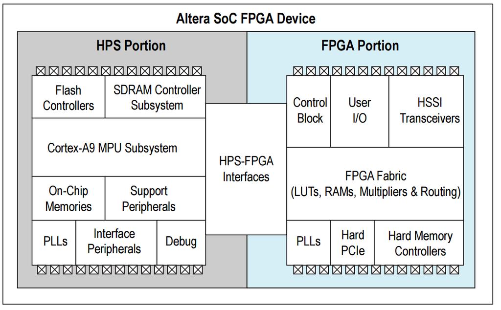
2 SOC + FPGA (ex. Cyclone V, Xilinx Zynq) New generation of FPGA include today FPGA parts Hardcore units System On Chip with programmable part for highly specialized systems on One Chip and high performance. 2
3 SOC + FPGA (ex.cyclonev) 4
4 SOC + FPGA (ex.cyclonev) 5
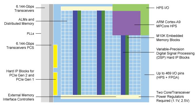
5 SOC + FPGA (ex. Cyclone V) FPGA part ALM (Adaptative Logic Module) 4 registers Many modes of operations: Normal mode Extended LUT mode Arithmetic mode Shared arithmetic mode Memory (M10k blocks) DSP (Digital Signal Processing) blocks 6
 32 x 2 Memory Block 4 registers RB 2015-2016")
6 ALM : Adaptative Logic Module ALM (Adaptative Logic Module) 32 x 2 Memory Block 4 registers RB
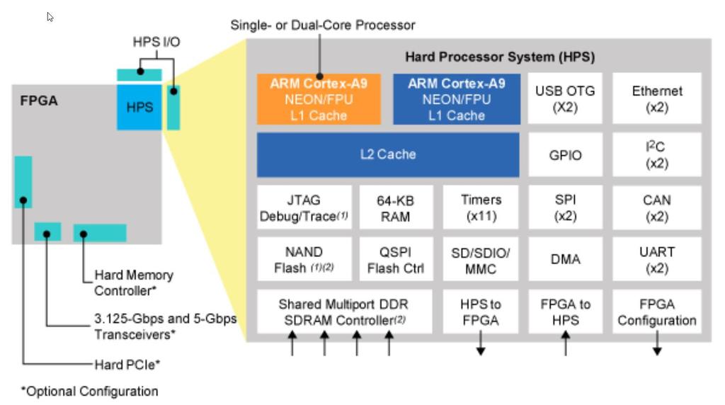
7 SOC + FPGA (ex. Cyclone V) Hardcore part 2 x ARM Cortex-A9 core + NEON SIMD coprocessor +FPU Snoop Control Unit (SCU) Accelerator Coherency Port (ACP) Many programmable interfaces External memory ctrl (DDRx) PCIe (opt.) High speed link (6.144 Gbps) (opt.) HPS I/O 8
8 SOC + FPGA (ex.cyclonev) 9
")
9 SOC + FPGA (ex.cyclonev) 12
 DDR3 SDRAM on HPS MICRO SD Card Socket on HPS Ethernet 10/100 Mbps VGA USB, http://www.terasic.")
10 DE1-SOC (Terasic) Board for test and laboratories Cyclone V SoC 5CSEMA5F31C6 Device 64 MB (32Mx16) SDRAM on FPGA 1 GB (2x256Mx16) DDR3 SDRAM on HPS MICRO SD Card Socket on HPS Ethernet 10/100 Mbps VGA USB, 13

11 DE1-SOC (Terasic) 14

12 DE1-SOC (Terasic) 15
")
13 SOC + FPGA (ex.cyclonev) 16
14 HPS Address Space HPS 3 address spaces L3 MPU SDRAM 17
15 HPS L3/MPU Address Space Region Name Description Base Address Size FPGA slaves FPGA slaves connected to the HPSto-FPGA bridge 0xC MB HPS peripherals Slaves directly connected to the HPS 0xFC MB Lightweight FPGA slaves FPGA slaves connected to the lightweight HPS-to-FPGA bridge 0xFF MB 18
16 HPS Peripheral Region Address Map Slave Identifier Slave Title Base Address Size STM STM 0xFC MB DAP DAP 0xFF MB LWFPGASLAVES FPGA slaves accessed with lightweight HPS-to-FPGA bridge 0xFF MB LWHPS2FPGAREGS Lightweight HPS-to-FPGA bridge GPV 0xFF MB HPS2FPGAREGS HPS-to-FPGA bridge GPV 0xFF MB FPGA2HPSREGS FPGA-to-HPS bridge GPV 0xFF MB EMAC0 EMAC0 0xFF KB EMAC1 EMAC1 0xFF KB SDMMC SD/MMC 0xFF KB QSPIREGS Quad SPI flash controller registers 0xFF KB FPGAMGRREGS FPGA manager registers 0xFF KB ACPIDMAP ACP ID mapper registers 0xFF KB GPIO0 GPIO0 0xFF KB GPIO1 GPIO1 0xFF KB GPIO2 GPIO2 0xFF70 A000 4 KB L3REGS L3 interconnect GPV 0xFF MB NANDDATA NAND controller data 0xFF MB QSPIDATA Quad SPI flash data 0xFFA MB USB0 USB0 OTG controller registers 0xFFB KB USB1 USB1 OTG controller registers 0xFFB KB NANDREGS NAND controller registers 0xFFB KB FPGAMGRDATA FPGA manager configuration data 0xFFB KB 19
17 HPS Peripheral Region Address Map Slave Identifier Slave Title Base Address Size CAN0 CAN0 controller registers 0xFFC KB CAN1 CAN1 controller registers 0xFFC KB UART0 UART0 0xFFC KB UART1 UART1 0xFFC KB I2C0 I2C0 0xFFC KB I2C1 I2C1 0xFFC KB I2C2 I2C2 0xFFC KB I2C3 I2C3 0xFFC KB SPTIMER0 SP Timer0 0xFFC KB SPTIMER1 SP Timer1 0xFFC KB SDRREGS SDRAM controller subsystem registers 0xFFC KB OSC1TIMER0 OSC1 Timer0 0xFFD KB OSC1TIMER1 OSC1 Timer1 0xFFD KB L4WD0 Watchdog0 0xFFD KB L4WD1 Watchdog1 0xFFD KB CLKMGR Clock manager 0xFFD KB RSTMGR Reset manager 0xFFD KB SYSMGR System manager 0xFFD KB DMANONSECURE DMA nonsecure registers 0xFFE KB DMASECURE DMA secure registers 0xFFE KB SPIS0 SPI slave0 0xFFE KB SPIS1 SPI slave1 0xFFE KB SPIM0 SPI master0 0xFFF KB SPIM1 SPI master1 0xFFF KB SCANMGR Scan manager registers 0xFFF KB ROM Boot ROM 0xFFFD KB MPUSCU MPU SCU registers 0xFFFE C000 8 KB MPUL2 MPU L2 cache controller registers 0xFFFE F000 4 KB OCRAM On-chip RAM 0xFFFF KB 20 RB
18 HPS Peripheral Region Address Map Two directories contain all HPS-related HEADER FILES: <altera_install_directory>/<version>/embedded/ip/altera/hps/ altera_hps/hwlib/include Contains HIGH-LEVEL header files that typically contain a few FUNCTIONS which facilitate control over the HPS components. These functions are all part of Altera s HWLIB, which was created to make programming the HPS easier. <altera_install_directory>/<version>/embedded/ip/altera/hps/ altera_hps/hwlib/include/socal Contains LOW-LEVEL header files that provide a peripheral s BIT-LEVEL REGISTER DETAILS. For example, any bits in a peripheral s register that correspond to undefined behavior will be specified in these header files. 21
19 HPS Peripheral Region Address Map /hwlib/include/alt_fpga_manager.h ALT_STATUS_CODE alt_fpga_reset_assert(void); ALT_STATUS_CODE alt_fpga_configure(const void* cfg_buf, size_t cfg_buf_len); /hwlib/include/socal/alt_fpgamgr.h /* The width in bits of the ALT_FPGAMGR_CTL_EN register field. */ #define ALT_FPGAMGR_CTL_EN_WIDTH 1 /* The mask used to set the ALT_FPGAMGR_CTL_EN register field value. */ #define ALT_FPGAMGR_CTL_EN_SET_MSK 0x /* The mask used to clear the ALT_FPGAMGR_CTL_EN register field value. */ #define ALT_FPGAMGR_CTL_EN_CLR_MSK 0xfffffffe 22
20 HPS Peripheral Region Address Map An important header file is /hwlib/include/socal/hps.h. It contains the HPS component s full REGISTER MAP Note that HWLIB can only be DIRECTLY used in a bare-metal application, or in a Linux device driver, as it directly references physical addresses. The linux kernel would terminate a user process that tries to access any of these addresses. 23
21 HPS Boot and FPGA Configuration The processor can boot from the following sources: NAND flash memory through the NAND flash controller SD/MMC flash memory through the SD/MMC flash controller (DE1-SOC board) SPI and QSPI flash memory through the QSPI flash controller using Slave Select 0 FPGA fabric on-chip memory Independent FPGA Configuration and HPS Booting 24
22 HPS Boot and FPGA Configuration FPGA Configuration before HPS Booting (HPS boots from FPGA) 25
23 HPS Boot and FPGA Configuration HPS Boots and Performs FPGA Configuration 26
24 HPS Boot Flows HPS Boot Flows Although the DE1-SoC has a DUAL-processor HPS: CPU1 is under reset, and the boot flow only executes on CPU0. To use both processors of the DE1-SoC, then USER SOFTWARE executing on CPU0 is responsible for releasing CPU1 from reset. 27
25 HPS Boot Flows The preloader typically performs the following actions: Initialize the SDRAM interface Configure the HPS I/O through the scan manager Configure pin multiplexing through the system manager Configure HPS clocks through the clock manager Initialize the flash controller (NAND, SD/MMC, QSPI) that contains the next stage boot software Load the next boot software into the SDRAM and pass control to it The preloader does NOT release CPU1 from reset. 28
26 Cyclone V, possible configurations the Cyclone V SoC can work in 3 different configurations: FPGA-only HPS-only HPS & FPGA For HPS applications: Bare-metal Application without OS Application over an Operating System as Linux 29
27 Cyclone V, project structure To help in the development process, suggested project structure: 31
28 Cyclone V, FPGA development process For the FPGA part, it s the same as for the others FPGA, Quartus II and Qsys tools NIOS II processor SDRAM Ctrl as softcore module Programmable Interface on Avalon Bus PLL for Clk and external SDRAM Clk 32

29 Cyclone V, FPGA development process 33
30 Cyclone V, HPS development process For the HPS part, it s the same as for the others FPGA, Quartus II and Qsys tools HPS configuration with Qsys I/O pins association 34
31 Cyclone V, HPS I/O selection From schematics: Ex.: HPS_KEY & HPS_LED In Qsys selection for the specifics pins: Mode GPIO: 35

32 Cyclone V, HPS I/O selection Ex.: HPS_KEY & HPS_LED GPIOXY: Configures the pin to be connected to the HPS GPIO peripheral. LOANIOXY: Configures the pin to be connected to the FPGA fabric. This pin can be exported from Qsys to be used by the FPGA. 36

33 Cyclone V, HPS FPGA development process 37
34 Cyclone V, HPS DDR3 configuration SDRAM Tab: In fact DDR3 memories Put the right parameters Assign the pins with tcl file 38
35 Cyclone V, Compilation Compilation Download through JTAG NIOS-SBT for NIOS programming ARM-DS-5 for ARM programming Exercice Follow the tutorial SOC-FPGA Design Guide 39
SoC-FPGA Design Guide DE0-Nano-SoC Edition
 SoC-FPGA Design Guide DE0-Nano-SoC Edition LAP IC EPFL Version 1.32 Sahand Kashani-Akhavan René Beuchat The latest version of this document (complete with all sources) can always be found in [26]. 1 TABLE
SoC-FPGA Design Guide
 SoC-FPGA Design Guide LAP IC EPFL Version 1.25 Sahand Kashani-Akhavan René Beuchat 1 TABLE OF CONTENTS 2 List of Figures... 6 3 Table of Tables... 8 4 Prerequisites... 9 4.1 Hardware... 9 4.2 Software...
Designing with ALTERA SoC Hardware
 Designing with ALTERA SoC Hardware Course Description This course provides all theoretical and practical know-how to design ALTERA SoC devices under Quartus II software. The course combines 60% theory
SoC Platforms and CPU Cores
 SoC Platforms and CPU Cores COE838: Systems on Chip Design http://www.ee.ryerson.ca/~courses/coe838/ Dr. Gul N. Khan http://www.ee.ryerson.ca/~gnkhan Electrical and Computer Engineering Ryerson University
Designing with ALTERA SoC
 Designing with ALTERA SoC תיאורהקורס קורסזהמספקאתכלהידע התיאורטיוהמעשילתכנוןרכיביSoC שלחברתALTERA תחתסביבת הפיתוחII.Quartus הקורסמשלב 60% תיאוריהו- 40% עבודה מעשית עללוחותפיתוח.SoC הקורסמתחילבסקירתמשפחותרכבי
Copyright 2016 Xilinx
 Zynq Architecture Zynq Vivado 2015.4 Version This material exempt per Department of Commerce license exception TSU Objectives After completing this module, you will be able to: Identify the basic building
Zynq Architecture, PS (ARM) and PL
 and PL") , PS (ARM) and PL Joint ICTP-IAEA School on Hybrid Reconfigurable Devices for Scientific Instrumentation Trieste, 1-5 June 2015 Fernando Rincón Fernando.rincon@uclm.es 1 Contents Zynq All Programmable
, PS (ARM) and PL Joint ICTP-IAEA School on Hybrid Reconfigurable Devices for Scientific Instrumentation Trieste, 1-5 June 2015 Fernando Rincón Fernando.rincon@uclm.es 1 Contents Zynq All Programmable
SoC FPGAs. Your User-Customizable System on Chip Altera Corporation Public
 SoC FPGAs Your User-Customizable System on Chip Embedded Developers Needs Low High Increase system performance Reduce system power Reduce board size Reduce system cost 2 Providing the Best of Both Worlds
Cyclone V SoC HPS Release Notes
 2014.12.15 RN-CVHPS Subscribe These release notes cover v. 13.0 through v. 14.1 of the Altera Cyclone V system on a chip (SoC) hard processor system (HPS). These release notes describe the following topics:
«Real Time Embedded systems» Multi Masters Systems
 «Real Time Embedded systems» Multi Masters Systems rene.beuchat@epfl.ch LAP/ISIM/IC/EPFL Chargé de cours rene.beuchat@hesge.ch LSN/hepia Prof. HES 1 Multi Master on Chip On a System On Chip, Master can
MYD-C7Z010/20 Development Board
 MYD-C7Z010/20 Development Board MYC-C7Z010/20 CPU Module as Controller Board Two 0.8mm pitch 140-pin Connectors for Board-to-Board Connections 667MHz Xilinx XC7Z010/20 Dual-core ARM Cortex-A9 Processor
MYC-C7Z010/20 CPU Module
 MYC-C7Z010/20 CPU Module - 667MHz Xilinx XC7Z010/20 Dual-core ARM Cortex-A9 Processor with Xilinx 7-series FPGA logic - 1GB DDR3 SDRAM (2 x 512MB, 32-bit), 4GB emmc, 32MB QSPI Flash - On-board Gigabit
Zynq-7000 All Programmable SoC Product Overview
 Zynq-7000 All Programmable SoC Product Overview The SW, HW and IO Programmable Platform August 2012 Copyright 2012 2009 Xilinx Introducing the Zynq -7000 All Programmable SoC Breakthrough Processing Platform
Embedded Systems. "System On Programmable Chip" NIOS II Avalon Bus. René Beuchat. Laboratoire d'architecture des Processeurs.
 Embedded Systems "System On Programmable Chip" NIOS II Avalon Bus René Beuchat Laboratoire d'architecture des Processeurs rene.beuchat@epfl.ch 3 Embedded system on Altera FPGA Goal : To understand the
Design of Embedded Hardware and Firmware
 Design of Embedded Hardware and Firmware Introduction on "System On Programmable Chip" NIOS II Avalon Bus - DMA Andres Upegui Laboratoire de Systèmes Numériques hepia/hes-so Geneva, Switzerland Embedded
Design Choices for FPGA-based SoCs When Adding a SATA Storage }
 U4 U7 U7 Q D U5 Q D Design Choices for FPGA-based SoCs When Adding a SATA Storage } Lorenz Kolb & Endric Schubert, Missing Link Electronics Rudolf Usselmann, ASICS World Services Motivation for SATA Storage
S2C K7 Prodigy Logic Module Series
 S2C K7 Prodigy Logic Module Series Low-Cost Fifth Generation Rapid FPGA-based Prototyping Hardware The S2C K7 Prodigy Logic Module is equipped with one Xilinx Kintex-7 XC7K410T or XC7K325T FPGA device
Cyclone V Device Overview
 Subscribe Send Feedback Latest document on the web: PDF HTML Contents Contents... 3 Key Advantages of Cyclone V Devices... 3 Summary of Cyclone V Features...4 Cyclone V Device Variants and Packages...
Cyclone V Device Overview
 2014.10.06 CV-51001 Subscribe The Cyclone V devices are designed to simultaneously accommodate the shrinking power consumption, cost, and time-to-market requirements; and the increasing bandwidth requirements
Nios II Embedded Design Suite Release Notes
 Nios II Embedded Design Suite Release Notes Subscribe Send Feedback Latest document on the web: PDF HTML Contents Contents 1...3 1.1 Product Revision History... 3 1.2 Nios II EDS v15.0 Updates...4 1.3
HPS SoC Boot Guide - Cyclone V SoC Development Kit
 2014.07.03 AN-709 Subscribe Introduction This document describes the available boot stages and source modes for both the HPS and FPGA fabric. The boot sequence is a multi-stage process, where each stage
FPGA Adaptive Software Debug and Performance Analysis
 white paper Intel Adaptive Software Debug and Performance Analysis Authors Javier Orensanz Director of Product Management, System Design Division ARM Stefano Zammattio Product Manager Intel Corporation
Cyclone V Device Overview
 CV-500 Subscribe Feedback The Cyclone V devices are designed to simultaneously accommodate the shrinking power consumption, cost, and time-to-market requirements; and the increasing bandwidth requirements
Qsys and IP Core Integration
 Qsys and IP Core Integration Stephen A. Edwards (after David Lariviere) Columbia University Spring 2016 IP Cores Altera s IP Core Integration Tools Connecting IP Cores IP Cores Cyclone V SoC: A Mix of
A. Booting and Configuration
 A. Booting and Configuration November 2012 cv_5400a-1.3 cv_5400a-1.3 This appendix describes the booting of the hard processor system (HPS) and the configuration of the FPGA portion of the Altera system-on-a-chip
ARM Cortex-A9 ARM v7-a. A programmer s perspective Part1
 ARM Cortex-A9 ARM v7-a A programmer s perspective Part1 ARM: Advanced RISC Machine First appeared in 1985 as Acorn RISC Machine from Acorn Computers in Manchester England Limited success outcompeted by
Embest SOC8200 Single Board Computer
 Embest SOC8200 Single Board Computer TI's AM3517 ARM Cortex A8 Microprocessors 600MHz ARM Cortex-A8 Core NEON SIMD Coprocessor POWERVR SGX Graphics Accelerator (AM3517 only) 16KB I-Cache, 16KB D-Cache,
NIOS CPU Based Embedded Computer System on Programmable Chip
 NIOS CPU Based Embedded Computer System on Programmable Chip 1 Lab Objectives EE8205: Embedded Computer Systems NIOS-II SoPC: PART-I This lab has been constructed to introduce the development of dedicated
Copyright 2014 Xilinx
 IP Integrator and Embedded System Design Flow Zynq Vivado 2014.2 Version This material exempt per Department of Commerce license exception TSU Objectives After completing this module, you will be able
1. Overview for the Arria V Device Family
 1. Overview for the Arria V Device Family December 2011 AV51001-1.2 AV51001-1.2 Built on the 28-nm low-power process technology, Arria V devices offer the lowest power and lowest system cost for mainstream
5. ARM 기반모니터프로그램사용. Embedded Processors. DE1-SoC 보드 (IntelFPGA) Application Processors. Development of the ARM Architecture.
 Application Processors. Development of the ARM Architecture.") Embedded Processors 5. ARM 기반모니터프로그램사용 DE1-SoC 보드 (IntelFPGA) 2 Application Processors Development of the ARM Architecture v4 v5 v6 v7 Halfword and signed halfword / byte support System mode Thumb instruction
Embedded Processors 5. ARM 기반모니터프로그램사용 DE1-SoC 보드 (IntelFPGA) 2 Application Processors Development of the ARM Architecture v4 v5 v6 v7 Halfword and signed halfword / byte support System mode Thumb instruction
University of Massachusetts Amherst Computer Systems Lab 1 (ECE 354) LAB 1 Reference Manual
 LAB 1 Reference Manual") University of Massachusetts Amherst Computer Systems Lab 1 (ECE 354) LAB 1 Reference Manual Lab 1: Using NIOS II processor for code execution on FPGA Objectives: 1. Understand the typical design flow in
University of Massachusetts Amherst Computer Systems Lab 1 (ECE 354) LAB 1 Reference Manual Lab 1: Using NIOS II processor for code execution on FPGA Objectives: 1. Understand the typical design flow in
MYD-C437X-PRU Development Board
 MYD-C437X-PRU Development Board MYC-C437X CPU Module as Controller Board Two 0.8mm pitch 100-pin Connectors for Board-to-Board Connections Up to 1GHz TI AM437x Series ARM Cortex-A9 Processors 512MB DDR3
Designing Embedded Processors in FPGAs
 Designing Embedded Processors in FPGAs 2002 Agenda Industrial Control Systems Concept Implementation Summary & Conclusions Industrial Control Systems Typically Low Volume Many Variations Required High
Avnet Zynq Mini Module Plus Embedded Design
 Avnet Zynq Mini Module Plus Embedded Design Version 1.0 May 2014 1 Introduction This document describes a Zynq standalone OS embedded design implemented and tested on the Avnet Zynq Mini Module Plus. 2
Intel SoC FPGA Embedded Development Suite (SoC EDS) Release Notes
 Release Notes") Intel SoC FPGA Embedded Development Suite (SoC EDS) Release Notes Updated for Intel Quartus Prime Design Suite: 18.1 Subscribe Latest document on the web: PDF HTML Contents Contents Intel SoC FPGA Embedded
Intel SoC FPGA Embedded Development Suite (SoC EDS) Release Notes Updated for Intel Quartus Prime Design Suite: 18.1 Subscribe Latest document on the web: PDF HTML Contents Contents Intel SoC FPGA Embedded
Designing with Nios II Processor for Hardware Engineers
 Designing with Nios II Processor for Hardware Engineers Course Description This course provides all theoretical and practical know-how to design ALTERA SoC FPGAs based on the Nios II soft processor under
Introduction to Sitara AM437x Processors
 Introduction to Sitara AM437x Processors AM437x: Highly integrated, scalable platform with enhanced industrial communications and security AM4376 AM4378 Software Key Features AM4372 AM4377 High-performance
Software Quality is Directly Proportional to Simulation Speed
 Software Quality is Directly Proportional to Simulation Speed CDNLive! 11 March 2014 Larry Lapides Page 1 Software Quality is Directly Proportional to Test Speed Intuitively obvious (so my presentation
Field Programmable Gate Array (FPGA) Devices
 Devices") Field Programmable Gate Array (FPGA) Devices 1 Contents Altera FPGAs and CPLDs CPLDs FPGAs with embedded processors ACEX FPGAs Cyclone I,II FPGAs APEX FPGAs Stratix FPGAs Stratix II,III FPGAs Xilinx FPGAs
Field Programmable Gate Array (FPGA) Devices 1 Contents Altera FPGAs and CPLDs CPLDs FPGAs with embedded processors ACEX FPGAs Cyclone I,II FPGAs APEX FPGAs Stratix FPGAs Stratix II,III FPGAs Xilinx FPGAs
1. Overview for Cyclone V Device Family
 1. Overview for Cyclone V Device Family November 2011 CV-51001-1.1 CV-51001-1.1 Cyclone V devices are designed to simultaneously accommodate the shrinking power consumption, cost, and time-to-market requirements;
Designing a Multi-Processor based system with FPGAs
 Designing a Multi-Processor based system with FPGAs BRINGING BRINGING YOU YOU THE THE NEXT NEXT LEVEL LEVEL IN IN EMBEDDED EMBEDDED DEVELOPMENT DEVELOPMENT Frank de Bont Trainer / Consultant Cereslaan
Intelop. *As new IP blocks become available, please contact the factory for the latest updated info.
 A FPGA based development platform as part of an EDK is available to target intelop provided IPs or other standard IPs. The platform with Virtex-4 FX12 Evaluation Kit provides a complete hardware environment
Bare Metal User Guide
 2015.11.30 UG-01165 Subscribe Introduction This guide will provide examples of how to create and debug Bare Metal projects using the ARM DS-5 Altera Edition included in the Altera SoC Embedded Design Suite
TOUGH. FAST. WHITE. introducing WHITEspeed. The groundbreaking Computer On Module. Designed & assembled by ERNI in Germany.
 TOUGH. FAST. WHITE. introducing WHITEspeed The groundbreaking Computer On Module. Designed & assembled by ERNI in Germany. introducing WHITEspeed TOUGH. FAST. WHITE. Computer On Module with Basic Board
MYD-JA5D2X Development Board
 MYD-JA5D2X Development Board MYC-JA5D2X CPU Module as Controller Board 500MHz Atmel SAMA5D26/27 ARM Cortex-A5 Processor 256MB DDR3 SDRAM, 256MB Nand Flash, 4MB Data FLASH, 64KB EEPROM Serial ports, USB,
MYD-SAMA5D3X Development Board
 MYD-SAMA5D3X Development Board MYC-SAMA5D3X CPU Module as Controller Board DDR2 SO-DIMM 200-pin Signals Consistent with Atmel's Official Board 536MHz Atmel SAMA5D3 Series ARM Cortex-A5 Processors 512MB
Product Technical Brief S3C2412 Rev 2.2, Apr. 2006
 Product Technical Brief S3C2412 Rev 2.2, Apr. 2006 Overview SAMSUNG's S3C2412 is a Derivative product of S3C2410A. S3C2412 is designed to provide hand-held devices and general applications with cost-effective,
Project Documentation
 2016 Project Documentation Configuration of SoC FPGA, Booting of HPS and running Bare Metal Application from SD card Supervisors: Dominique GIGI Awais Zahid Rasheed CERN Summer Student 9/6/2016 Petr Zejdl
Intel Stratix 10 SoC FPGA Boot User Guide
 Intel Stratix 10 SoC FPGA Boot User Guide Updated for Intel Quartus Prime Design Suite: 18.1 Subscribe Latest document on the web: PDF HTML Contents Contents 1. Introduction... 4 1.1. Glossary...4 1.2.
RK3036 Kylin Board Hardware Manual V0.1
 RK3036 Kylin Board Hardware Manual V0.1 Content 1 Introduction 1.1 Kylin at first glance 1.2 Boot to console 1.3 Key features 1.4 Block diagram 2 Key parts in details 2.1 Processor 2.2 Memory 2.3 Storage
Cyclone V SoC PCI-Express Root Port Example Design. Application Note
 Cyclone V SoC PCI-Express Root Port Example Design Application Note 7/1/2013 Table of Contents 1 Revision History... 4 2 Overview... 5 2.1 GSRD... 5 3 Hardware and Software Packages... 6 3.1 GSRD... 6
Product Technical Brief S3C2416 May 2008
 Product Technical Brief S3C2416 May 2008 Overview SAMSUNG's S3C2416 is a 32/16-bit RISC cost-effective, low power, high performance micro-processor solution for general applications including the GPS Navigation
Simulation Based Analysis and Debug of Heterogeneous Platforms
 Simulation Based Analysis and Debug of Heterogeneous Platforms Design Automation Conference, Session 60 4 June 2014 Simon Davidmann, Imperas Page 1 Agenda Programming on heterogeneous platforms Hardware-based
High-Performance, Highly Secure Networking for Industrial and IoT Applications
 High-Performance, Highly Secure Networking for Industrial and IoT Applications Table of Contents 2 Introduction 2 Communication Accelerators 3 Enterprise Network Lineage Features 5 Example applications
FPQ6 - MPC8313E implementation
 Formation MPC8313E implementation: This course covers PowerQUICC II Pro MPC8313 - Processeurs PowerPC: NXP Power CPUs FPQ6 - MPC8313E implementation This course covers PowerQUICC II Pro MPC8313 Objectives
Product Technical Brief S3C2440X Series Rev 2.0, Oct. 2003
 Product Technical Brief S3C2440X Series Rev 2.0, Oct. 2003 S3C2440X is a derivative product of Samsung s S3C24XXX family of microprocessors for mobile communication market. The S3C2440X s main enhancement
AT-501 Cortex-A5 System On Module Product Brief
 AT-501 Cortex-A5 System On Module Product Brief 1. Scope The following document provides a brief description of the AT-501 System on Module (SOM) its features and ordering options. For more details please
Product Technical Brief S3C2413 Rev 2.2, Apr. 2006
 Product Technical Brief Rev 2.2, Apr. 2006 Overview SAMSUNG's is a Derivative product of S3C2410A. is designed to provide hand-held devices and general applications with cost-effective, low-power, and
MYC-C437X CPU Module
 MYC-C437X CPU Module - Up to 1GHz TI AM437x Series ARM Cortex-A9 Processors - 512MB DDR3 SDRAM, 4GB emmc Flash, 32KB EEPROM - Gigabit Ethernet PHY - Power Management IC - Two 0.8mm pitch 100-pin Board-to-Board
ECE 471 Embedded Systems Lecture 3
 ECE 471 Embedded Systems Lecture 3 Vince Weaver http://web.eece.maine.edu/~vweaver vincent.weaver@maine.edu 10 September 2018 Announcements New classroom: Stevens 365 HW#1 was posted, due Friday Reminder:
EMAC SoM Presentation.
 EMAC SoM Presentation www.emacinc.com www.emacinc.com/som System on Module System on Module (SoM) is an alternative to Single Board Computers for Embedded Systems offering a more flexible & contoured solution.
1 Do not confuse the MPU with the Nios II memory management unit (MMU). The MPU does not provide memory mapping or management.
. The MPU does not provide memory mapping or management.") Nios II MPU Usage March 2010 AN-540-1.0 Introduction This application note covers the basic features of the Nios II processor s optional memory protection unit (MPU), describing how to use it without the
Nios II MPU Usage March 2010 AN-540-1.0 Introduction This application note covers the basic features of the Nios II processor s optional memory protection unit (MPU), describing how to use it without the
Lesson 6 Intel Galileo and Edison Prototype Development Platforms. Chapter-8 L06: "Internet of Things ", Raj Kamal, Publs.: McGraw-Hill Education
 Lesson 6 Intel Galileo and Edison Prototype Development Platforms 1 Intel Galileo Gen 2 Boards Based on the Intel Pentium architecture Includes features of single threaded, single core and 400 MHz constant
SOM PRODUCTS BRIEF. S y s t e m o n M o d u l e. Engicam. SOMProducts ver
 SOM S y s t e m o n M o d u l e PRODUCTS BRIEF GEA M6425IB ARM9 TM Low cost solution Reduced Time to Market Very small form factor Low cost multimedia solutions Industrial Automotive Consumer Single power
Laboratory Exercise 5
 Laboratory Exercise 5 Bus Communication The purpose of this exercise is to learn how to communicate using a bus. In the designs generated by using Altera s SOPC Builder, the Nios II processor connects
Cyclone V SoCs. Automotive Safety Manual. 101 Innovation Drive San Jose, CA MNL Subscribe Send Feedback
 Cyclone V SoCs Automotive Safety Manual Subscribe MNL-1079 101 Innovation Drive San Jose, CA 95134 www.altera.com TOC-2 Cyclone V SoCs Automotive Safety Manual Contents Introduction to Cyclone V SoCs and
EyeCheck Smart Cameras
 EyeCheck Smart Cameras 2 3 EyeCheck 9xx & 1xxx series Technical data Memory: DDR RAM 128 MB FLASH 128 MB Interfaces: Ethernet (LAN) RS422, RS232 (not EC900, EC910, EC1000, EC1010) EtherNet / IP PROFINET
ARM Powered SoCs OpenEmbedded: a framework for toolcha. generation and rootfs management
 ARM Powered SoCs OpenEmbedded: a framework for toolchain generation and rootfs management jacopo @ Admstaff Reloaded 12-2010 An overview on commercial ARM-Powered SOCs Many low-cost ARM powered devices
Partial Reconfiguration with the Arria 10 HPS
 2017.01.25 AN-798 Subscribe Partial reconfiguration (PR) allows you to reconfigure a portion of the FPGA dynamically, while the remaining FPGA design continues to function. With partial reconfiguration,
Intel Stratix 10 SoC FPGA Boot User Guide
 Intel Stratix 10 SoC FPGA Boot User Guide Updated for Intel Quartus Prime Design Suite: 18.0 Subscribe Send Feedback Latest document on the web: PDF HTML Contents Contents... 3 Glossary... 3 Prerequisites...
ARM Cortex-M4 Architecture and Instruction Set 1: Architecture Overview
 ARM Cortex-M4 Architecture and Instruction Set 1: Architecture Overview M J Brockway January 25, 2016 UM10562 All information provided in this document is subject to legal disclaimers. NXP B.V. 2014. All
Embedded Design Handbook
 Subscribe Send Feedback Latest document on the web: PDF HTML Contents Contents 1 Introduction... 6 1.1 Document Revision History... 6 2 First Time Designer's Guide... 7 2.1 FPGAs and Soft-Core Processors...
Early Software Development Through Emulation for a Complex SoC
 Early Software Development Through Emulation for a Complex SoC FTF-NET-F0204 Raghav U. Nayak Senior Validation Engineer A P R. 2 0 1 4 TM External Use Session Objectives After completing this session you
Hardware Specification. Figure 1-2 ZYNQ-7000 Device Family 2 / 9
 Z-turn Board 667MHz Xilinx XC7Z010/20 Dual-core ARM Cortex-A9 Processor with Xilinx 7-series FPGA logic 1GB DDR3 SDRAM (2 x 512MB, 32-bit), 16MB SPI Flash USB_UART, USB2.0 OTG, 1 x 10/100/1000Mbps Ethernet,
EMAC SoM Presentation
 EMAC SoM Presentation www.emacinc.com www.emacinc emacinc.com/.com/som System on Module System on Module (SoM( SoM) ) is an alternative to Single Board Computers for Embedded Systems offering a more flexible
pcduino V3B XC4350 User Manual
 pcduino V3B XC4350 User Manual 1 User Manual Contents Board Overview...2 System Features...3 Single-Board Computer Configuration......3 Pin Assignments...4 Single-Board Computer Setup...6 Required Hardware...6
MYD-IMX28X Development Board
 MYD-IMX28X Development Board MYC-IMX28X CPU Module as Controller Board Two 1.27mm pitch 80-pin SMT Male Connectors for Board-to-Board Connections 454MHz Freescale i.mx28 Series ARM926EJ-S Processors 128MB
MYD-Y6ULX Development Board
 MYD-Y6ULX Development Board MYC-Y6ULX CPU Module as Controller Board 528Hz NXP i.mx 6UL/6ULL ARM Cortex-A7 Processors 1.0mm pitch 140-pin Stamp Hole Expansion Interface for Board-to-Board Connections 256MB
Zynq AP SoC Family
 Programmable Logic (PL) Processing System (PS) Zynq -7000 AP SoC Family Cost-Optimized Devices Mid-Range Devices Device Name Z-7007S Z-7012S Z-7014S Z-7010 Z-7015 Z-7020 Z-7030 Z-7035 Z-7045 Z-7100 Part
MYD-IMX28X Development Board
 MYD-IMX28X Development Board MYC-IMX28X CPU Module as Controller Board Two 1.27mm pitch 80-pin SMT Connectors for Board-to-Board Connections 454MHz Freescale i.mx28 Series ARM926EJ-S Processors 128MB DDR2
BlazePPS (Blaze Packet Processing System) CSEE W4840 Project Design
 CSEE W4840 Project Design") BlazePPS (Blaze Packet Processing System) CSEE W4840 Project Design Valeh Valiollahpour Amiri (vv2252) Christopher Campbell (cc3769) Yuanpei Zhang (yz2727) Sheng Qian ( sq2168) March 26, 2015 I) Hardware
BlazePPS (Blaze Packet Processing System) CSEE W4840 Project Design Valeh Valiollahpour Amiri (vv2252) Christopher Campbell (cc3769) Yuanpei Zhang (yz2727) Sheng Qian ( sq2168) March 26, 2015 I) Hardware
Graduate Institute of Electronics Engineering, NTU Advanced VLSI SOPC design flow
 Advanced VLSI SOPC design flow Advisor: Speaker: ACCESS IC LAB What s SOC? IP classification IP reusable & benefit Outline SOPC solution on FPGA SOPC design flow pp. 2 What s SOC? Definition of SOC Advantage
Requirement ZYNQ SOC Development Board: Z-Turn by MYiR ZYNQ-7020 (XC7Z020-1CLG400C) Vivado and Xilinx SDK TF Card Reader (Micro SD) Windows 7
 Vivado and Xilinx SDK TF Card Reader (Micro SD) Windows 7") Project Description The ARM CPU is configured to perform read and write operations on the Block Memory. The Block Memory is created in the PL side of the ZYNQ device. The ARM CPU is configured as Master
Project Description The ARM CPU is configured to perform read and write operations on the Block Memory. The Block Memory is created in the PL side of the ZYNQ device. The ARM CPU is configured as Master
. Micro SD Card Socket. SMARC 2.0 Compliant
 MSC SM2S-IMX6 NXP i.mx6 ARM Cortex -A9 Description The design of the MSC SM2S-IMX6 module is based on NXP s i.mx 6 processors offering quad-, dual- and single-core ARM Cortex -A9 compute performance at
Designing with NXP i.mx8m SoC
 Designing with NXP i.mx8m SoC Course Description Designing with NXP i.mx8m SoC is a 3 days deep dive training to the latest NXP application processor family. The first part of the course starts by overviewing
CoreTile Express for Cortex-A5
 CoreTile Express for Cortex-A5 For the Versatile Express Family The Versatile Express family development boards provide an excellent environment for prototyping the next generation of system-on-chip designs.
Full Linux on FPGA. Sven Gregori
 Full Linux on FPGA Sven Gregori Enclustra GmbH FPGA Design Center Founded in 2004 7 engineers Located in the Technopark of Zurich FPGA-Vendor independent Covering all topics
KeyStone C665x Multicore SoC
 KeyStone Multicore SoC Architecture KeyStone C6655/57: Device Features C66x C6655: One C66x DSP Core at 1.0 or 1.25 GHz C6657: Two C66x DSP Cores at 0.85, 1.0, or 1.25 GHz Fixed and Floating Point Operations
Parallella Linux - quickstart guide. Antmicro Ltd
 Parallella Linux - quickstart guide Antmicro Ltd June 13, 2016 Contents 1 Introduction 1 1.1 Xilinx tools.......................................... 1 1.2 Version information.....................................
ZC706 Built-In Self Test Flash Application April 2015
 ZC706 Built-In Self Test Flash Application April 2015 XTP242 Revision History Date Version Description 04/30/15 11.0 Recompiled for 2015.1. 11/24/14 10.0 Recompiled for 2014.4. 10/08/14 9.0 Recompiled
ESP32 Technical Reference Manual. Espressif Systems
 ESP32 Technical Reference Manual Espressif Systems August 31, 216 About This Manual ESP32 Technical Reference Manual targets application developers. The manual provides detailed and complete information
DevKit8500D Evaluation Kit
 DevKit8500D Evaluation Kit TI DM3730 Processor based on 800MHz ARM Cortex-A8 core Onboard 512MByte DDR SDRAM and 512MByte NAND Flash 3 UART, 4 USB Host, USB OTG, Ethernet, Audio, TF, Keyboard, Jtag,...
Introduction to Embedded System Design using Zynq
 Introduction to Embedded System Design using Zynq Zynq Vivado 2015.2 Version This material exempt per Department of Commerce license exception TSU Objectives After completing this module, you will be able
Porting VME-Based Optical-Link Remote I/O Module to a PLC Platform - an Approach to Maximize Cross-Platform Portability Using SoC
 Porting VME-Based Optical-Link Remote I/O Module to a PLC Platform - an Approach to Maximize Cross-Platform Portability Using SoC T. Masuda, A. Kiyomichi Japan Synchrotron Radiation Research Institute
Zynq-7000 All Programmable SoC: Concepts, Tools, and Techniques (CTT)
") Zynq-7000 All Programmable SoC: Concepts, Tools, and Techniques (CTT) A Hands-On Guide to Effective Embedded System Design Notice of Disclaimer The information disclosed to you hereunder (the Materials
Zynq-7000 All Programmable SoC: Concepts, Tools, and Techniques (CTT) A Hands-On Guide to Effective Embedded System Design Notice of Disclaimer The information disclosed to you hereunder (the Materials
DevKit7000 Evaluation Kit
 DevKit7000 Evaluation Kit Samsung S5PV210 Processor based on 1GHz ARM Cortex-A8 core Onboard 512MByte DDR2 and 512MByte NAND Flash 4 UART, 4 USB Host, USB Device, Ethernet, Audio, TF, RTC,... Supports
XMC-ZU1. XMC Module Xilinx Zynq UltraScale+ MPSoC. Overview. Key Features. Typical Applications
 XMC-ZU1 XMC Module Xilinx Zynq UltraScale+ MPSoC Overview PanaTeQ s XMC-ZU1 is a XMC module based on the Zynq UltraScale+ MultiProcessor SoC device from Xilinx. The Zynq UltraScale+ integrates a Quad-core
Zet x86 open source SoC
 http://zet.aluzina.org v1.1 19 Feb 2010 Contents 1 2 Contents 1 2 Terasic Altera DE1 - Cyclone II FPGA http://www.terasic.com.tw Physical devices 1 FPGA 2 SDRAM 3 SRAM 4 Flash 5 SD card 6 VGA 7 50 Mhz
EMBEDDED HARDWARE. Core Board. ARM7 Development board. ARM7 Evaluation Board. Page 1 of 5
 Core Board * Size: 71.2mm *50.8mm * Industrial grade 32-bit RISC micro-controller * Mass storage device support * Industrial grade 16C550 Serial Interface * 10/100M Industrial Ethernet interface * USB