FPGA.
|
|
|
- Dwayne Clifford Long
- 6 years ago
- Views:
Transcription


1
2 CMOS TTL Verilog VHDL


3 7400. NAND CMOS TTL 1 0 source sink datasheet bounce


4 bounce debunce RS Latch debounce Typical Characteristics NO NC Semiconductor Material Wavelength Colour V 20mA NOR NAND GaAs nm Infra- Red 1.2v bounce GaAsP nm Red 1.8v bounce GaAsP nm Amber 2.0v GaAsP:N nm Yellow 2.2v AlGaP nm Green 3.5v SiC nm Blue 3.6v GaInN 450nm White 4.0v 0 1 CMOS (source) (standard) (sink) TTL 7400 kω Vcc
5 Vcc Ω 1 High Low 1 0 debounce 7400 RS Latch NAND
6 NOT OR AND carry Reset Load clock clock clock load reset clock load reset clock load reset clock clock look-ahead-carry


")


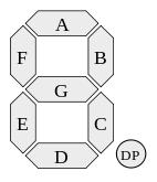
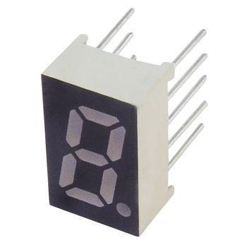
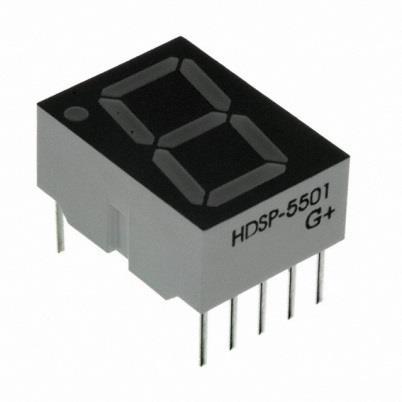
7 NOT OR AND seg seg 7segment seven segment 9 0 dp g f e d c b a 7seg (Common Anode) (Common Cathode) 7seg 7seg 7seg k
8
9 reset clk (load) reset khz ms khz (time-base) b a b khz a b BCD Hz reset b b khz a ms 7seg reset Hz Hz
10 (time-base) Hz Hz 74283


11 BCD BCD to 7segment
12 don t care FSM ASM BCD 74153


13 A/D 1 Latch D/A DAC D/A R/2R (R) V od kω kω ADC A/D A/D S&H A/D
14 (successive approximations) R/2R D/A A/D start conversion D/A start conversion D/A A/D


 7 6 5 4 3 2 1 0")


15 x Vcc active low low low active low load enable x = x 1 3 = (low) low reset set reset
16


17 (3S400-PQ208) Spartan 3 SDRAM Dip-Switch MHz (RS232) USB DAC ADC Flash ROM ROM JTAg Xilinx ISE clear VHDL code for 7-segment drive library ieee; use ieee.std_logic_1164.all; use ieee.std_logic_arith.all; use ieee.std_logic_unsigned.all; entity svnsegdrv is port ( din : in std_logic_vector (3 downto 0); segs : out std_logic_vector (7 downto 0));
18 end svnsegdrv; architecture behavioral of svnsegdrv is --file produced for nasre shargh fpga board --input : 4 bits are normally located : left msb, right lsb begin -- abcdefgdp common cathode -- with din select -- segs <= " " when "0000", -- " " when "0001", -- " " when "0010", -- " " when "0011", -- " " when "0100", -- " " when "0101", -- " " when "0110", -- " " when "0111", -- " " when "1000", -- " " when "1001", -- " " when "1010", -- " " when "1011", -- " " when "1100", -- " " when "1101", -- " " when "1110", -- " " when "1111", -- " " when others; with din select -- abcdefgdp common anode segs <= " " when "0000", " " when "0001", " " when "0010", " " when "0011", " " when "0100", " " when "0101", " " when "0110", " " when "0111", " " when "1000", " " when "1001", " " when "1010", " " when "1011", " " when "1100", " " when "1101", " " when "1110", " " when "1111", " " when others; end behavioral;
19 MHz AM/PM dip-switch MHz khz VHDL code for clock library ieee; use ieee.std_logic_1164.all; use ieee.std_logic_arith.all; use ieee.std_logic_unsigned.all; entity clock2 is port ( clk : in std_logic; csel : in std_logic_vector (2 downto 0); yml : out std_logic_vector (7 downto 0); ymh : out std_logic_vector (7 downto 0); yhl : out std_logic_vector (7 downto 0); yhh : out std_logic_vector (7 downto 0); ampm : out std_logic);
20 end clock2; architecture behavioral of clock2 is component svnsegdrv port( din : in std_logic_vector(3 downto 0); segs : out std_logic_vector(7 downto 0) ); end component; signal d0 : std_logic_vector(3 downto 0) := (others => '0'); signal d1 : std_logic_vector(3 downto 0) := (others => '0'); signal d2 : std_logic_vector(3 downto 0) := (others => '0'); signal d3 : std_logic_vector(3 downto 0) := (others => '0'); signal c : std_logic_vector(27 downto 0) := (others => '0'); signal ck : std_logic; signal sampm : std_logic := '0'; begin process(clk, ck) begin if rising_edge(clk) then --ck'event and clk='1' then c<=c+1; end if; if rising_edge(ck) then if d0="1001" then d0 <= (others => '0'); if d1="0101" then d1 <= (others => '0'); if d2="1001" or (d2="0001" and d3="0001") then d2 <= (others => '0'); if d3="0001" then d3 <= (others => '0'); sampm <= not sampm; else d3<=d3+1; end if; else d2<=d2+1; end if; else d1<=d1+1; end if; else d0<=d0+1; end if; end if; end process; dd0: svnsegdrv port map(din => d0, segs => yml ); dd1: svnsegdrv port map(din => d1, segs => ymh ); dd2: svnsegdrv port map(din => d2, segs => yhl ); dd3: svnsegdrv port map(din => d3, segs => yhh ); ampm <= sampm; ck <= c(23) when (csel(0)='1') else c(20) when (csel(1)='1') else c(17) when (csel(2)='1') else c(14); end behavioral;
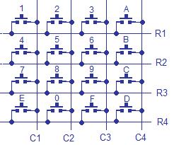
21 VHDL VHDL hex n n-bit x n-bit.ucf ucf pull-up.ucf VHDL code for keypad decoding library ieee; use ieee.std_logic_1164.all; use ieee.std_logic_arith.all; use ieee.std_logic_unsigned.all; entity clock2 is
22 port ( clk : in std_logic; column : in std_logic_vector (3 downto 0); csel : in std_logic_vector (2 downto 0); row : out std_logic_vector (3 downto 0); y : out std_logic_vector (7 downto 0); cout : out std_logic_vector (7 downto 0); ampm : out std_logic); end clock2; architecture behavioral of clock2 is begin component svnsegdrv port( din : in std_logic_vector(3 downto 0); segs : out std_logic_vector(7 downto 0) ); end component; signal count : std_logic_vector(3 downto 0) := (others => '0'); signal reg : std_logic_vector(3 downto 0) := (others => '0'); signal decode : std_logic_vector(3 downto 0) := (others => '0'); signal c : std_logic_vector(27 downto 0) := (others => '0'); signal ck : std_logic; signal regclk : std_logic := '0'; process(clk) begin if rising_edge(clk) then --ck'event and clk='1' then c<=c+1; end if; end process; process(ck) begin if rising_edge(ck) then if count="1111" then count <= (others => '0'); else count<=count+1; end if; if regclk='1' then reg <= count; end if; end if; end process; process (count(1 downto 0),column(0),column(1),column(2),column(3)) begin case count(1 downto 0) is when "00" => regclk <= not column(0); when "01" => regclk <= not column(1); when "10" => regclk <= not column(2); when "11" => regclk <= not column(3); when others => regclk <= not column(0); end case; end process; dd0: svnsegdrv port map(din => count, segs => cout ); dd1: svnsegdrv port map(din => reg, segs => y ); ck <= c(23) when (csel(0)='1') else c(20) when (csel(1)='1') else c(17) when (csel(2)='1') else c(14); with count(3 downto 2) select row <= "0111" when "00", "1011" when "01", "1101" when "10", "1110" when others;
23 end behavioral;
24 BCD truncation
25 BCD BCD BCD BCD BCD n BCD function Destination (BCD) x100 x10 x1 Source (binary) start state shift # shift # shift #3, 7> add with result shift #4, 5> add with result shift # shift #6, 6> add with result shift #7, 7> add with result shift # n n m m BCD m BCD BCD BCD BCD


26 ascii bps bps dipswitch bps RS232 0 start bit 1 stop bit parity 1 idle 1 bps D D RS232
27 0 1 start idle stop 1 framing error 0 parity error dipswitch bps ascii bps bps
28 o o o (busy)
29
Field Programmable Gate Array
 Field Programmable Gate Array System Arch 27 (Fire Tom Wada) What is FPGA? System Arch 27 (Fire Tom Wada) 2 FPGA Programmable (= reconfigurable) Digital System Component Basic components Combinational
In our case Dr. Johnson is setting the best practices
 VHDL Best Practices Best Practices??? Best practices are often defined by company, toolset or device In our case Dr. Johnson is setting the best practices These rules are for Class/Lab purposes. Industry
Design Examples. ELEC 418 Advanced Digital Systems Dr. Ron Hayne. Images Courtesy of Cengage Learning
 Design Examples ELEC 418 Advanced Digital Systems Dr. Ron Hayne Images Courtesy of Cengage Learning BCD to 7-Segment Display 418_04 2 BCD to 7-Segment Display entity BCD_Seven is port(bcd: in std_logic_vector(3
Lab 3: Standard Combinational Components
 Lab 3: Standard Combinational Components Purpose In this lab you will implement several combinational circuits on the DE1 development board to test and verify their operations. Introduction Using a high-level
ACS College of Engineering. Department of Biomedical Engineering. Logic Design Lab pre lab questions ( ) Cycle-1
 Cycle-1") ACS College of Engineering Department of Biomedical Engineering Logic Design Lab pre lab questions (2015-2016) Cycle-1 1. What is a combinational circuit? 2. What are the various methods of simplifying
ACS College of Engineering Department of Biomedical Engineering Logic Design Lab pre lab questions (2015-2016) Cycle-1 1. What is a combinational circuit? 2. What are the various methods of simplifying
EEE8076. Reconfigurable Hardware Design (coursework) Module Outline. Dr A. Bystrov Dr. E.G. Chester. Autumn
 Module Outline. Dr A. Bystrov Dr. E.G. Chester. Autumn") EEE8076 Reconfigurable Hardware Design (coursework) Module Outline Dr A. Bystrov Dr. E.G. Chester Autumn 2010 1 2 3 4 5 6 7 8 9 10 11 12 Altera UP2 development board, Flex EPF10K70 FPGA www.altera.com/literature/univ/upds.pdf
EEE8076 Reconfigurable Hardware Design (coursework) Module Outline Dr A. Bystrov Dr. E.G. Chester Autumn 2010 1 2 3 4 5 6 7 8 9 10 11 12 Altera UP2 development board, Flex EPF10K70 FPGA www.altera.com/literature/univ/upds.pdf
CSE 260 Introduction to Digital Logic and Computer Design. Exam 1. Your name 2/13/2014
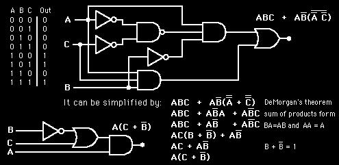
 CSE 260 Introduction to Digital Logic and Computer Design Jonathan Turner Exam 1 Your name 2/13/2014 1. (10 points) Draw a logic diagram that implements the expression A(B+C)(C +D)(B+D ) directly (do not
EENG 2910 Project III: Digital System Design. Due: 04/30/2014. Team Members: University of North Texas Department of Electrical Engineering
 EENG 2910 Project III: Digital System Design Due: 04/30/2014 Team Members: University of North Texas Department of Electrical Engineering Table of Content i Contents Abstract...3 Introduction...3 Report...4
EITF35 - Introduction to the Structured VLSI Design (Fall 2016) Interfacing Keyboard with FPGA Board. (FPGA Interfacing) Teacher: Dr.
 Interfacing Keyboard with FPGA Board. (FPGA Interfacing) Teacher: Dr.") EITF35 - Introduction to the Structured VLSI Design (Fall 2016) Interfacing Keyboard with FPGA Board (FPGA Interfacing) Teacher: Dr. Liang Liu v.1.0.0 1 Abstract This document describes the basic behavior
EITF35 - Introduction to the Structured VLSI Design (Fall 2016) Interfacing Keyboard with FPGA Board (FPGA Interfacing) Teacher: Dr. Liang Liu v.1.0.0 1 Abstract This document describes the basic behavior
13/06/56 8 ก ก. 08-Case Study
 8 ก ก ก 1 ก 2 1 3 VHDL DIVIDER200Hz use IEEE.std_logic_1164.all; entity DIVIDER200Hz is generic (fin: integer :=25000000; --Input frequency fout: integer :=200); --Output frequency end DIVIDER200Hz; architecture
Design Problem 3 Solutions
 CSE 260 Digital Computers: Organization and Logical Design Jon Turner Design Problem 3 Solutions In this problem, you are to design, simulate and implement a sequential pattern spotter, using VHDL. This
Digital System Construction
 Digital System Construction FYSIKUM Lecture 4: More VHDL, memory, PRNG Arithmetic Memories Pipelines and buffers Pseudorandom numbers IP core generation in Vivado Introduction to Lab 3 Digital Systemkonstruktion
8-1. Fig. 8-1 ASM Chart Elements 2001 Prentice Hall, Inc. M. Morris Mano & Charles R. Kime LOGIC AND COMPUTER DESIGN FUNDAMENTALS, 2e, Updated.
 8-1 Name Binary code IDLE 000 Register operation or output R 0 RUN 0 1 Condition (a) State box (b) Example of state box (c) Decision box IDLE R 0 From decision box 0 1 START Register operation or output
DIGITAL LOGIC DESIGN VHDL Coding for FPGAs Unit 6
 DIGITAL LOGIC DESIGN VHDL Coding for FPGAs Unit 6 FINITE STATE MACHINES (FSMs) Moore Machines Mealy Machines Algorithmic State Machine (ASM) charts FINITE STATE MACHINES (FSMs) Classification: Moore Machine:
Board-Data Processing. VHDL Exercises. Exercise 1: Basics of VHDL Programming. Stages of the Development process using FPGA s in Xilinx ISE.
 Board-Data Processing VHDL Exercises Exercise 1: Basics of VHDL Programming Stages of the Development process using FPGA s in Xilinx ISE. Basics of VHDL VHDL (Very High Speed IC Hardware description Language)
LABORATORY MANUAL VLSI DESIGN LAB EE-330-F
 LABORATORY MANUAL VLSI DESIGN LAB EE-330-F (VI th Semester) Prepared By: Vikrant Verma B. Tech. (ECE), M. Tech. (ECE) Department of Electrical & Electronics Engineering BRCM College of Engineering & Technology
ELCT 501: Digital System Design
 ELCT 501: Digital System Lecture 4: CAD tools (Continued) Dr. Mohamed Abd El Ghany, Basic VHDL Concept Via an Example Problem: write VHDL code for 1-bit adder 4-bit adder 2 1-bit adder Inputs: A (1 bit)
Introduction to VHDL #1
 ECE 3220 Digital Design with VHDL Introduction to VHDL #1 Lecture 3 Introduction to VHDL The two Hardware Description Languages that are most often used in industry are: n VHDL n Verilog you will learn
Lecture 7. Standard ICs FPGA (Field Programmable Gate Array) VHDL (Very-high-speed integrated circuits. Hardware Description Language)
 VHDL (Very-high-speed integrated circuits. Hardware Description Language)") Standard ICs FPGA (Field Programmable Gate Array) VHDL (Very-high-speed integrated circuits Hardware Description Language) 1 Standard ICs PLD: Programmable Logic Device CPLD: Complex PLD FPGA: Field Programmable
Standard ICs FPGA (Field Programmable Gate Array) VHDL (Very-high-speed integrated circuits Hardware Description Language) 1 Standard ICs PLD: Programmable Logic Device CPLD: Complex PLD FPGA: Field Programmable
LCD Display. Other I/O. LCD display Flash ROM SPI EPROM Keyboard (PS/2) UART connectors DAC ADC. 2-line, 16 character LCD display
 UART connectors DAC ADC. 2-line, 16 character LCD display") Other I/O LCD display Flash ROM SPI EPROM Keyboard (PS/2) UART connectors DAC ADC LCD Display 2-line, 16 character LCD display 4-bit interface Relatively easy to use once you have it mapped into your processor
Other I/O LCD display Flash ROM SPI EPROM Keyboard (PS/2) UART connectors DAC ADC LCD Display 2-line, 16 character LCD display 4-bit interface Relatively easy to use once you have it mapped into your processor
Control and Datapath 8
 Control and Datapath 8 Engineering attempts to develop design methods that break a problem up into separate steps to simplify the design and increase the likelihood of a correct solution. Digital system
Sequential Statement
 Sequential Statement Sequential Logic Output depends not only on current input values but also on previous input values. Are building blocks of; Counters Shift registers Memories Flip flops are basic sequential
ECE 545 Lecture 12. FPGA Resources. George Mason University
 ECE 545 Lecture 2 FPGA Resources George Mason University Recommended reading 7 Series FPGAs Configurable Logic Block: User Guide Overview Functional Details 2 What is an FPGA? Configurable Logic Blocks
Sign here to give permission for your test to be returned in class, where others might see your score:
 EEL 4712 Midterm 2 Spring 216 VERSION 1 Name: UFID: Sign here to give permission for your test to be returned in class, where others might see your score: IMPORTANT: Please be neat and write (or draw)
VHDL And Synthesis Review
 VHDL And Synthesis Review VHDL In Detail Things that we will look at: Port and Types Arithmetic Operators Design styles for Synthesis VHDL Ports Four Different Types of Ports in: signal values are read-only
Example 15: Moving Sprites with Flash Background
 Displaying an Image Read from Flash Memory 95 Listing 2.5 (cont.) vga_flash_n2_top.vhd clr
DIGITAL LOGIC WITH VHDL (Fall 2013) Unit 1
 Unit 1") DIGITAL LOGIC WITH VHDL (Fall 23) Unit DESIGN FLOW DATA TYPES LOGIC GATES WITH VHDL TESTBENCH GENERATION DESIGN FLOW Design Entry: We specify the logic circuit using a Hardware Description Language (e.g.,
DIGITAL LOGIC WITH VHDL (Fall 23) Unit DESIGN FLOW DATA TYPES LOGIC GATES WITH VHDL TESTBENCH GENERATION DESIGN FLOW Design Entry: We specify the logic circuit using a Hardware Description Language (e.g.,
Contents. Chapter 9 Datapaths Page 1 of 28
 Chapter 9 Datapaths Page of 2 Contents Contents... 9 Datapaths... 2 9. General Datapath... 3 9.2 Using a General Datapath... 5 9.3 Timing Issues... 7 9.4 A More Complex General Datapath... 9 9.5 VHDL for
Sequential Logic - Module 5
 Sequential Logic Module 5 Jim Duckworth, WPI 1 Latches and Flip-Flops Implemented by using signals in IF statements that are not completely specified Necessary latches or registers are inferred by the
5. 0 VHDL OPERATORS. The above classes are arranged in increasing priority when parentheses are not used.
 Filename= ch5.doc 5. 0 VHDL OPERATORS There are seven groups of predefined VHDL operators: 1. Binary logical operators: and or nand nor xor xnor 2. Relational operators: = /= < >= 3. Shifts operators:
3e library declarations library IEEE; use IEEE.std_logic_1164.all;
 3e8.54 XSvhd.4Please see the VHDL program below or in the accompanying.zip file (if published by your instructor). This program was kindly written and contributed by Xilinx application engineering, but
VHDL. ELEC 418 Advanced Digital Systems Dr. Ron Hayne. Images Courtesy of Cengage Learning
 VHDL ELEC 418 Advanced Digital Systems Dr. Ron Hayne Images Courtesy of Cengage Learning Design Flow 418_02 2 VHDL Modules 418_02 3 VHDL Libraries library IEEE; use IEEE.std_logic_1164.all; std_logic Single-bit
VHDL: Modeling RAM and Register Files. Textbook Chapters: 6.6.1, 8.7, 8.8, 9.5.2, 11.2
 VHDL: Modeling RAM and Register Files Textbook Chapters: 6.6.1, 8.7, 8.8, 9.5.2, 11.2 Memory Synthesis Approaches: Random logic using flip-flops or latches Register files in datapaths RAM standard components
Part 4: VHDL for sequential circuits. Introduction to Modeling and Verification of Digital Systems. Memory elements. Sequential circuits
 M1 Informatique / MOSIG Introduction to Modeling and erification of Digital Systems Part 4: HDL for sequential circuits Laurence PIERRE http://users-tima.imag.fr/amfors/lpierre/m1arc 2017/2018 81 Sequential
Schedule. ECE U530 Digital Hardware Synthesis. Rest of Semester. Midterm Question 1a
 ECE U530 Digital Hardware Synthesis Prof. Miriam Leeser mel@coe.neu.edu November 8, 2006 Midterm Average: 70 Lecture 16: Midterm Solutions Homework 6: Calculator Handshaking HW 6: Due Wednesday, November
Solutions - Homework 4 (Due date: November 9:30 am) Presentation and clarity are very important!
 Presentation and clarity are very important!") DPARTMNT OF LCTRICAL AND COMPUTR NGINRING, TH UNIVRSITY OF NW MXICO C-38L: Computer Logic Design Fall 3 Solutions - Homework 4 (Due date: November 6th @ 9:3 am) Presentation and clarity are very important!
DPARTMNT OF LCTRICAL AND COMPUTR NGINRING, TH UNIVRSITY OF NW MXICO C-38L: Computer Logic Design Fall 3 Solutions - Homework 4 (Due date: November 6th @ 9:3 am) Presentation and clarity are very important!
Chapter 6 Combinational-Circuit Building Blocks
 Chapter 6 Combinational-Circuit Building Blocks Commonly used combinational building blocks in design of large circuits: Multiplexers Decoders Encoders Comparators Arithmetic circuits Multiplexers A multiplexer
EITF35: Introduction to Structured VLSI Design
 EITF35: Introduction to Structured VLSI Design Part 2.2.2: VHDL-3 Liang Liu liang.liu@eit.lth.se 1 Outline Inference of Basic Storage Element Some Design Examples DFF with enable Counter Coding Style:
The VHDL Hardware Description Language
 The VHDL Hardware Description Language p. 1/? The VHDL Hardware Description Language CSEE W4840 Prof. Stephen A. Edwards Columbia University The VHDL Hardware Description Language p. 2/? Why HDLs? 1970s:
Pollard s Tutorial on Clocked Stuff in VHDL
 Pollard s Tutorial on Clocked Stuff in VHDL Welcome to a biased view of how to do register type of stuff in VHDL. The object of this short note is to identify one way to easily handle registered logic
CHAPTER NINE - MSI Logic Circuits
 CHAPTER NINE - MSI Logic Circuits 9. (a) All of the outputs are HIGH. (b) O =, O- O7 = (c) O - O6 =, O7 =. (d) Same as (a). 9.2 Inputs = 6: Outputs = 64 9.3 (a) [ O6] -> A2=, A=, A=, E3=, E2 =, E= (b)
Summary of FPGA & VHDL
 FYS4220/9220 Summary of FPGA & VHDL Lecture #6 Jan Kenneth Bekkeng, University of Oslo - Department of Physics 16.11.2011 Curriculum (VHDL & FPGA part) Curriculum (Syllabus) defined by: Lectures Lecture6:
[VARIABLE declaration] BEGIN. sequential statements
![[VARIABLE declaration] BEGIN. sequential statements](/thumbs/89/98890993.jpg "[VARIABLE declaration] BEGIN. sequential statements") PROCESS statement (contains sequential statements) Simple signal assignment statement
PROCESS statement (contains sequential statements) Simple signal assignment statement
VHDL Testbench. Test Bench Syntax. VHDL Testbench Tutorial 1. Contents
 VHDL Testbench Tutorial 1 Contents 1 VHDL Testbench 2 Test Bench Syntax 3 Testbench Example: VHDL Code for Up Down Binary Counter 4 VHDL Testbench code for up down binary counter 5 Testbench Waveform for
The University of Alabama in Huntsville ECE Department CPE Final Exam Solution Spring 2004
 The University of Alabama in Huntsville ECE Department CPE 526 01 Final Exam Solution Spring 2004 1. (15 points) An old Thunderbird car has three left and three right tail lights, which flash in unique
Reconfigurable Hardware Design (coursework)
") EEE8076 Reconfigurable Hardware Design (coursework) Dr A. Bystrov Dr. E.G. Chester Autumn 2010 Module Outline Teaching Staff Dr Alex Bystrov Dr Graeme Chester The contact details are in the EECE web page
EEE8076 Reconfigurable Hardware Design (coursework) Dr A. Bystrov Dr. E.G. Chester Autumn 2010 Module Outline Teaching Staff Dr Alex Bystrov Dr Graeme Chester The contact details are in the EECE web page
The goal of this project is to design an FPGA-based cipher unit for the Xilinx Spartan II XC2S100 FPGA running on the XESS board.
 Project #5: Simple cipher unit with letter frequency counter Assigned: 11/11/2003 Due: 12/09/2003 (Hard deadline, no extensions.) To be completed in groups of two. The goal of this project is to design
EECE 353: Digital Systems Design Lecture 10: Datapath Circuits
 EECE 353: Digital Systems Design Lecture 10: Datapath Circuits Cristian Grecu grecuc@ece.ubc.ca Course web site: http://courses.ece.ubc.ca/353 Introduction to lecture 10 Large digital systems are more
HDL. Hardware Description Languages extensively used for:
 HDL Hardware Description Languages extensively used for: Describing (digital) hardware (formal documentation) Simulating it Verifying it Synthesizing it (first step of modern design flow) 2 main options:
CSE 260 Introduction to Digital Logic and Computer Design. Exam 1 Solutions
 CSE 6 Introduction to igital Logic and Computer esign Exam Solutions Jonathan Turner /3/4. ( points) raw a logic diagram that implements the expression (B+C)(C +)(B+ ) directly (do not simplify first),
PINE TRAINING ACADEMY
 PINE TRAINING ACADEMY Course Module A d d r e s s D - 5 5 7, G o v i n d p u r a m, G h a z i a b a d, U. P., 2 0 1 0 1 3, I n d i a Digital Logic System Design using Gates/Verilog or VHDL and Implementation
XSA Parallel Port Interface
 November 16, 2001 (Version 1.0) Application Note by D. Vanden Bout Summary This application note describes the default parallel port interface circuit that is programmed into the XC9572XL CPLD on the XSA
ECE 545 Lecture 11 Addendum
 ECE 545 Lecture 11 Addendum Controllers for Keccak_F and AES George Mason University ECE 448 FPGA and ASIC Design with VHDL Keccak_F 1600 din start done Keccak_F rst 1600 dout ready Note: Bold line represents
VHDL in 1h. Martin Schöberl
 VHDL in 1h Martin Schöberl VHDL /= C, Java, Think in hardware All constructs run concurrent Different from software programming Forget the simulation explanation VHDL is complex We use only a small subset
8-1. Fig. 8-1 ASM Chart Elements 2001 Prentice Hall, Inc. M. Morris Mano & Charles R. Kime LOGIC AND COMPUTER DESIGN FUNDAMENTALS, 2e, Updated.
 8-1 Name Binary code IDLE 000 Register operation or output R 0 RUN Condition (a) State box (b) Example of state box (c) Decision box IDLE R 0 From decision box START Register operation or output PC 0 (d)
Problem Set 10 Solutions
 CSE 260 Digital Computers: Organization and Logical Design Problem Set 10 Solutions Jon Turner thru 6.20 1. The diagram below shows a memory array containing 32 words of 2 bits each. Label each memory
CprE 583 Reconfigurable Computing
 Recap Moore FSM Example CprE / ComS 583 Reconfigurable Computing Moore FSM that recognizes sequence 10 0 1 0 1 S0 / 0 S1 / 0 1 S2 / 1 Prof. Joseph Zambreno Department of Electrical and Computer Engineering
Chip Design with FPGA Design Tools
 Chip Design with FPGA Design Tools Intern: Supervisor: Antoine Vazquez Janusz Zalewski Florida Gulf Coast University Fort Myers, FL 33928 V1.9, August 28 th. Page 1 1. Introduction FPGA is abbreviation
Lab 3. Advanced VHDL
 Lab 3 Advanced VHDL Lab 3 Advanced VHDL This lab will demonstrate many advanced VHDL techniques and how they can be used to your advantage to create efficient VHDL code. Topics include operator balancing,
4I39 RS-422 ANYTHING I/O MANUAL
 4I39 RS-422 ANYTHING I/O MANUAL V1.0 Table of Contents GENERAL.......................................................... 1 DESCRIPTION................................................. 1 HARDWARE CONFIGURATION........................................
Design a 4 bit-adder. Then design a 4-7 decoder to show the outputs. Output Sum(4 bits) Adder. Output carry(1 bit)
 Adder. Output carry(1 bit)") Csc 343 Lab 2 Sep 28. 07 Objective: Design a 4 bit-adder. Then design a 4-7 decoder to show the outputs. Structure: Input A (4 bits) Input B (4 bit) Adder Output Sum(4 bits) Output carry(1 bit) input cin
Csc 343 Lab 2 Sep 28. 07 Objective: Design a 4 bit-adder. Then design a 4-7 decoder to show the outputs. Structure: Input A (4 bits) Input B (4 bit) Adder Output Sum(4 bits) Output carry(1 bit) input cin
entity priority is Port ( a,b,c,d : in STD_LOGIC; encoded : out STD_LOGIC_VECTOR(2 downto 0)); end priority;
); end priority;") Примери Приоритетен кодер library IEEE; use IEEE.STD_LOGIC_1164.ALL; entity priority is Port ( a,b,c,d : in STD_LOGIC; encoded : out STD_LOGIC_VECTOR(2 downto 0)); end priority; architecture Behavioral
Примери Приоритетен кодер library IEEE; use IEEE.STD_LOGIC_1164.ALL; entity priority is Port ( a,b,c,d : in STD_LOGIC; encoded : out STD_LOGIC_VECTOR(2 downto 0)); end priority; architecture Behavioral
Lecture 5: State Machines, Arrays, Loops. EE 3610 Digital Systems
 EE 3610: Digital Systems 1 Lecture 5: State Machines, Arrays, Loops BCD to Excess-3 (XS 3 ) Code Converter Example: Fig. 2-53 2 Easier to use one type of code (e.g. XS 3 ) over the other type (e.g. BCD)
Control Unit: Binary Multiplier. Arturo Díaz-Pérez Departamento de Computación Laboratorio de Tecnologías de Información CINVESTAV-IPN
 Control Unit: Binary Multiplier Arturo Díaz-Pérez Departamento de Computación Laboratorio de Tecnologías de Información CINVESTAV-IPN Example: Binary Multiplier Two versions Hardwired control Microprogrammed
Advanced Electronics Lab.
 College of Engineering Course Book of 2010-2011 Advanced Electronics Lab. Mr. Araz Sabir Ameen M.Sc. in Electronics & Communications ALTERA DE2 Development and Education Board DE2 Package: The DE2 package
Today. Comments about assignment Max 1/T (skew = 0) Max clock skew? Comments about assignment 3 ASICs and Programmable logic Others courses
 Max clock skew? Comments about assignment 3 ASICs and Programmable logic Others courses") Today Comments about assignment 3-43 Comments about assignment 3 ASICs and Programmable logic Others courses octor Per should show up in the end of the lecture Mealy machines can not be coded in a single
Today Comments about assignment 3-43 Comments about assignment 3 ASICs and Programmable logic Others courses octor Per should show up in the end of the lecture Mealy machines can not be coded in a single
Computer-Aided Digital System Design VHDL
 بس م اهلل الر حم ن الر حی م Iran University of Science and Technology Department of Computer Engineering Computer-Aided Digital System Design VHDL Ramin Rajaei ramin_rajaei@ee.sharif.edu Modeling Styles
Quartus Counter Example. Last updated 9/6/18
 Quartus Counter Example Last updated 9/6/18 Create a logic design from start to a DE10 implementation This example uses best design practices This example is not about creating HDL The HDL code will be
PALMiCE FPGA Probing Function User's Manual
 PALMiCE FPGA Probing Function User's Manual This manual describes the probing function and presents the basic usage patterns. Chapter1 Introducing the Probing Function The probing function makes it easy
Mid-Term Exam Solutions
 CS/EE 26 Digital Computers: Organization and Logical Design Mid-Term Eam Solutions Jon Turner 3/3/3. (6 points) List all the minterms for the epression (B + A)C + AC + BC. Epanding the epression gives
Converting Hardware Interface Layer (HIL) v1.x Projects to v2.0
 v1.x Projects to v2.0") HUNT ENGINEERING Chestnut Court, Burton Row, Brent Knoll, Somerset, TA9 4BP, UK Tel: (+44) (0)1278 760188, Fax: (+44) (0)1278 760199, Email: sales@hunteng.co.uk www.hunteng.co.uk www.hunt-dsp.com Converting
HUNT ENGINEERING Chestnut Court, Burton Row, Brent Knoll, Somerset, TA9 4BP, UK Tel: (+44) (0)1278 760188, Fax: (+44) (0)1278 760199, Email: sales@hunteng.co.uk www.hunteng.co.uk www.hunt-dsp.com Converting
Learning about VHDL & FPGA s
 DE NAYER Instituut J. De Nayerlaan 5 B-2860 Sint-Katelijne-Waver Tel. (015) 31 69 44 Fax. (015) 31 74 53 e-mail: ppe@denayer.wenk.be ddr@denayer.wenk.be tti@denayer.wenk.be pvp@denayer.wenk.be website:
ECE 459/559 Secure & Trustworthy Computer Hardware Design
 ECE 459/559 Secure & Trustworthy Computer Hardware Design VHDL Overview Garrett S. Rose Spring 2016 Recap Public Key Encryption (PKE) RSA (Rivest, Shamir and Adelman) Encryption Advanced Encryption Standard
ECE 448 Lecture 13. FPGA Memories. George Mason University
 ECE 448 Lecture 13 FPGA Memories George Mason University Recommended reading Spartan-6 FPGA Block RAM Resources: User Guide Google search: UG383 Spartan-6 FPGA Configurable Logic Block: User Guide Google
FSM Components. FSM Description. HDL Coding Methods. Chapter 7: HDL Coding Techniques
 FSM Components XST features: Specific inference capabilities for synchronous Finite State Machine (FSM) components. Built-in FSM encoding strategies to accommodate your optimization goals. You may also
Lecture 12 VHDL Synthesis
 CPE 487: Digital System Design Spring 2018 Lecture 12 VHDL Synthesis Bryan Ackland Department of Electrical and Computer Engineering Stevens Institute of Technology Hoboken, NJ 07030 1 What is Synthesis?
CS303 LOGIC DESIGN FINAL EXAM
 JANUARY 2017. CS303 LOGIC DESIGN FINAL EXAM STUDENT NAME & ID: DATE: Instructions: Examination time: 100 min. Write your name and student number in the space provided above. This examination is closed
CCE 3202 Advanced Digital System Design
 CCE 3202 Advanced Digital System Design Lab Exercise #2 This lab exercise will show you how to create, synthesize, and test a 3-bit ripple counter. A ripple counter is simply a circuit that outputs the
Getting Started with VHDL
 Getting Started with VHDL VHDL code is composed of a number of entities Entities describe the interface of the component Entities can be primitive objects or complex objects Architectures are associated
Lecture 1: VHDL Quick Start. Digital Systems Design. Fall 10, Dec 17 Lecture 1 1
 Lecture 1: VHDL Quick Start Digital Systems Design Fall 10, Dec 17 Lecture 1 1 Objective Quick introduction to VHDL basic language concepts basic design methodology Use The Student s Guide to VHDL or The
Example 58: Traffic Lights
 208 Chapter 8 Listing 8.7(cont.) doorlock2_top.vhd btn012
COE Design Process Tutorial
 COE 758 - Design Process Tutorial I. Introduction This tutorial describes a formal design process for the creation of digital systems. The aim of this design process is to provide a systematic approach
RTC Interface 89C51 DS M. Krishna Kumar MAM/M7/LU17/V1/ Vcc VCC 5 SDA P1.0 6 SCL P KHz 3 BAT 3.
 RTC Interface 89C51 Vcc P1.0 10k 10k 5 SDA DS 1307 8 VCC P1.1 6 SCL X1 1 + 3 BAT X2 2 32.768KHz - 3.6V 4 GND INTB\SQW 7 M. Krishna Kumar MAM/M7/LU17/V1/2004 1 RTC Interface contd. DS 1307 is a real time
Chapter 2 68HC11 Based Temperature Monitoring Board
 Chapter 2 68HC11 Based Temperature Monitoring Board Before we discuss the testing approach, it is helpful to know the system on which it is being applied. In this chapter, we will describe the design and
DIGITAL LOGIC WITH VHDL (Fall 2013) Unit 3
 Unit 3") DIGITAL LOGIC WITH VHDL (Fall 2013) Unit 3 BEHAVIORAL DESCRIPTION Asynchronous processes (decoder, mux, encoder, etc): if-else, case, for-loop. BEHAVIORAL DESCRIPTION (OR SEQUENTIAL) In this design style,
DIGITAL LOGIC WITH VHDL (Fall 2013) Unit 3 BEHAVIORAL DESCRIPTION Asynchronous processes (decoder, mux, encoder, etc): if-else, case, for-loop. BEHAVIORAL DESCRIPTION (OR SEQUENTIAL) In this design style,
DIGITAL LOGIC WITH VHDL (Fall 2013) Unit 6
 Unit 6") DIGITAL LOGIC WITH VHDL (Fall 2013) Unit 6 FINITE STATE MACHINES (FSMs) Moore Machines Mealy Machines FINITE STATE MACHINES (FSMs) Classification: Moore Machine: Outputs depend only on the current state
DIGITAL LOGIC WITH VHDL (Fall 2013) Unit 6 FINITE STATE MACHINES (FSMs) Moore Machines Mealy Machines FINITE STATE MACHINES (FSMs) Classification: Moore Machine: Outputs depend only on the current state
Lab 4: Integrating a picoblaze processor in LabVIEW FPGA by use of CLIP node
 Lab 4: Integrating a picoblaze processor in LabVIEW FPGA by use of CLIP node Keywords: LabVIEW, LabVIEW FPGA, Xilinx SPARTAN3E Starter Kit, VHDL, picoblaze, assembler, CLIP node. Introduction Welcome to
Xilinx Spartan3E-100 CP132
 Basys2 Board Reference Manual Revision: November 11, 2010 1300 Henley Court Pullman, WA 99163 (509) 33 6306 Voice and Fax Introduction The Basys2 board is a circuit design and implementation platform that
Inferring Storage Elements
 Inferring Storage Elements In our designs, we usually use flip-flops as our storage elements. Sometimes we use latches, but not often. Latches are smaller in size, but create special, often difficult situations
Topics. Midterm Finish Chapter 7
 Lecture 9 Topics Midterm Finish Chapter 7 ROM (review) Memory device in which permanent binary information is stored. Example: 32 x 8 ROM Five input lines (2 5 = 32) 32 outputs, each representing a memory
Interfacing a PS/2 Keyboard
 Lab 3 in SMD52 Interfacing a PS/2 Keyboard Introduction In this lab you will interface a PS/2 keyboard (standard PC keyboard) with the XSB board. Scan codes will be received from the keyboard and displayed
Basic Concepts. Task One: The Basic Latch. Laboratory Nine Latches, RAM & Android Architecture
 Laboratory Nine Latches, RAM & Android Architecture Basic Concepts 1. The most basic element of binary storage is the latch, consisting of 2 cross-coupled NAND (or NOR) gates. 2. The D-latch with Enable
ECE 448 Lecture 4. Sequential-Circuit Building Blocks. Mixing Description Styles
 ECE 448 Lecture 4 Sequential-Circuit Building Blocks Mixing Description Styles George Mason University Reading Required P. Chu, FPGA Prototyping by VHDL Examples Chapter 4, Regular Sequential Circuit Recommended
CPE 626 Advanced VLSI Design Lecture 6: VHDL Synthesis. Register File: An Example. Register File: An Example (cont d) Aleksandar Milenkovic
 Aleksandar Milenkovic") CPE 626 Lecture 6: VHDL Synthesis Aleksandar Milenkovic http://www.ece.uah.edu/~milenka http://www.ece.uah.edu/~milenka/cpe626-04f/ milenka@ece.uah.edu Assistant Professor Electrical and Computer Engineering
CPE 626 Lecture 6: VHDL Synthesis Aleksandar Milenkovic http://www.ece.uah.edu/~milenka http://www.ece.uah.edu/~milenka/cpe626-04f/ milenka@ece.uah.edu Assistant Professor Electrical and Computer Engineering
INTRODUCTION TO VHDL ADVANCED COMPUTER ARCHITECTURES. Slides by: Pedro Tomás. Additional reading: - ARQUITECTURAS AVANÇADAS DE COMPUTADORES (AAC)
") INTRODUCTION TO VHDL Slides by: Pedro Tomás Additional reading: - ADVANCED COMPUTER ARCHITECTURES ARQUITECTURAS AVANÇADAS DE COMPUTADORES (AAC) Outline 2 Hardware Description Languages (HDL) VHDL Very
INTRODUCTION TO VHDL Slides by: Pedro Tomás Additional reading: - ADVANCED COMPUTER ARCHITECTURES ARQUITECTURAS AVANÇADAS DE COMPUTADORES (AAC) Outline 2 Hardware Description Languages (HDL) VHDL Very
EEL 4712 Digital Design Test 1 Spring Semester 2008
 IMPORTANT: Please be neat and write (or draw) carefully. If we cannot read it with a reasonable effort, it is assumed wrong. Also, as always, the best answer gets the most points. COVER SHEET: Problem:
Systems Programming. Lecture 2 Review of Computer Architecture I
 Systems Programming www.atomicrhubarb.com/systems Lecture 2 Review of Computer Architecture I In The Book Patt & Patel Chapter 1,2,3 (review) Outline Binary Bit Numbering Logical operations 2's complement
Introduction to VHDL Design on Quartus II and DE2 Board
 ECP3116 Digital Computer Design Lab Experiment Duration: 3 hours Introduction to VHDL Design on Quartus II and DE2 Board Objective To learn how to create projects using Quartus II, design circuits and
Guidelines for Laboratory Sessions:
 University of Malta Faculty of Engineering Department of Electronic Systems Engineering Hardware Description Languages ELE 3103 Lecturer: Dr. Ivan Grech igrech@eng.um.edu.mt Laboratory Tutors: Dr. Edward
Logic Implementation on a Xilinx FPGA using VHDL WWU Linux platform assumed. rev 10/25/16
 1 Logic Implementation on a Xilinx FPGA using VHDL WWU Linux platform assumed. rev 10/25/16 The following is a general outline of steps (i.e. design flow) used to implement a digital system described with