Introduction to Digital Design with Verilog HDL
|
|
|
- Oliver Craig
- 5 years ago
- Views:
Transcription
1 Introduction to Digital Design with Verilog HDL Modeling Styles 1
2 Levels of Abstraction n Behavioral The highest level of abstraction provided by Verilog HDL. A module is implemented in terms of the desired design algorithm n Data Flow At this level the module is designed by specifying the data flow n Gate Level The module is implemented in terms of logic gates and interconnections between these gates n Switch Level This is the lowest level of abstraction provided by Verilog. A module can be implemented in terms of switches, storage nodes and the interconnections between them 2
3 Behavioral Modeling n Behavioral modeling n Data flow modeling n Gate level modeling n Switch level modeling n Others 3
4 Behavioral Modeling n Blocks always Event-based timing control Branch case, casex, casez 4
5 Behavioral Modeling: always Block Syntax always operation_name module pulse; reg clock; Example // start the clock at 0 initial clock = 1'b0; /* toggle every 10 time units*/ always #10 clock = ~clock; endmodule 5
6 Behavioral Modeling: Event-based Timing Control Syntax (clock) a = b; when the clock changes value, execute a = (negedge clock) a = b; when the clock change to a 0, execute a=b a clock) b; evaluate b immediately and assign to a on a po sitive clock edge. 6
7 Behavioral Modeling: Branch Statements Syntax if (conditional_expression) statement1 else statement2 Example if (x!=1) a=2; else a=5; 7
8 Behavioral Modeling: Case Syntax case(op) op1:operation1 op2:operation2 op3:operation3 op4:operation4 default:operation5 endcase Example case(s3) 00:A=00 01:A=01 10:A=10 11:A=11 default:operation5 endcase 8
9 Behavioral Modeling: casex, casez n Two variations of the case statement casez Treats all z values in the case alternatives or the case expression as don't cares, all bit positions with z can also be represented by? in that position casex Treats all x and z values in the case item or the case expression as don't cares reg [3:0] encoding; integer state; casex (encoding) 4'b1xxx : next_state = 3; 4'bx1xx : next_state = 2; 4'bxx1x : next_state = 1; 4'bxxx1 : next_state = 0; default : next_state = 0; endcase An input encoding = 4'b10xz would cause next_state = 3 to be executed 9
10 Behavioral Modeling n Definition of blocking and non-blocking procedural assignments n Delay-based timing control mechanism in behavioral modeling n The significance of structured procedures always and initial in behavioral modeling n Event-based timing control mechanism in behavioral modeling n Level-sensitive timing control mechanism in behavioral modeling n Conditional statements using if and else n Multiway branching, using case, casex, and casez statements n Looping statements while, for, repeat, and forever n Sequential and parallel blocks 10
11 Procedural Assignments n Update values of reg, integer, real, or time variables Blocking Non-blocking 11
12 Procedural Assignments: Blocking n Blocking assignment statements are executed in the order they are specified in a sequential block n A blocking assignment will not block execution of statements that follow in a parallel block n The = operator is used to specify blocking assignments reg x, y, z; reg [15:0] reg_a, reg_b; integer count; initial begin end x = 0; y = 1; z = 1; // time 0 count = 0; // time 0 reg_a = 16'b0; // time 0 reg_b = reg_a; // time 0 #15 reg_a[2] = 1'b1; // time 15 #10 reg_b[15:13] = {x, y, z}; // time 25 count = count + 1; // time 25 12
13 Procedural Assignments: Non-Blocking n Non-blocking assignments allow scheduling of assignments without blocking execution of the statements that follow in a sequential block n A <= operator is used to specify non-blocking assignments reg x, y, z; reg [15:0] reg_a, reg_b; integer count; initial begin x = 0; y = 1; z = 1; // time 0 count = 0; // time 0 reg_a = 16'b0; // time 0 reg_b = reg_a; // time 0 reg_a[2] <= #15 1'b1; // time 0, but assigned at time 15 reg_b[15:13] <= #10 {x, y, z}; // time 0, but assigned at time 10 count <= count + 1; // time 0, assigned at time 0 end 13

14 Blocking vs. Nonblocking Assignments 14

15 Assignment Styles for Sequential Logic 15
16 Use Nonblocking for Sequential Logic 16
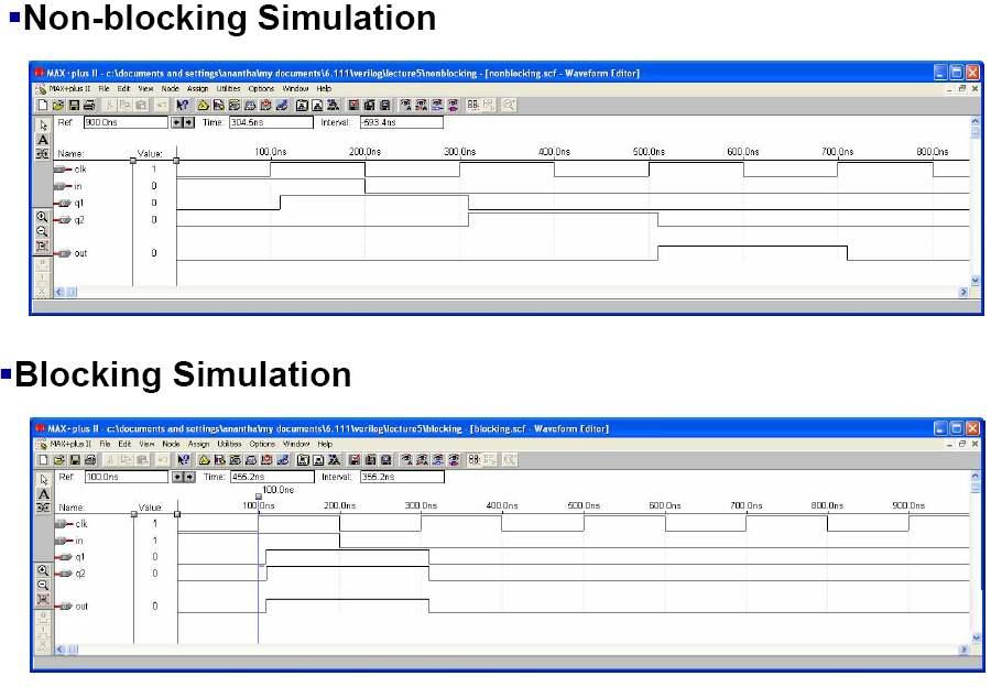
17 Simulation 17

18 Use Blocking for Combinational Logic 18
19 The Sequential always Block 19

20 Importance of the Sensitivity List 20
21 Simulation 21
22 Design a 4 to 1 MUX Using if Statement module multiplexor4_1 (out, in1, in2, in3,in4, cntrl1, cntrl2); output out; input in1, in2, in3, in4, cntrl1, cntrl2; reg out; // Note that this is now a register or in2 or in3 or in4 or cntrl1 or cntrl2) if (cntrl1==1) if (cntrl2==1) out = in4; else out = in3; else if (cntrl2==1) out = in2; else out = in1; endmodule 22
23 Design a 4 to 1 MUX using case Statement module multiplexor4_1 (out, in1, in2, in3, in4, cntrl1, cntrl2); output out; input in1, in2, in3, in4, cntrl1, cntrl2; reg out; // note must be a register in2 in3 in4 cntrl1 cntrl2) case ({cntrl2, cntrl1}) // concatenation 2'b00 : out = in1; 2'b01 : out = in2; 2'b10 : out = in3; 2'b11 : out = in4; default : $display("please check control bits"); endcase endmodule 23
24 Data Flow Modeling n Behavioral modeling n Data flow modeling n Gate level modeling n Switch level modeling n Others 24
25 Data Flow Modeling n Describe the continuous assignment (assign) statement n Assignment delay, implicit assignment delay, net declaration delay n Expressions, operators, operands (already mentioned) n Examples of digital circuits modeling in Verilog 25
26 assign Statement n assign out = in1 & in2; Continuous assign Out is a net i1 and i2 are nets n assign addit[15:0] = addit1[15:0] ^ addit2[15:0]; Continuous assign for vector nets, addr is a 16 bit vector net Addi1 and addit2 are 16-bit vector registers n assign {cout, sum[3:0]} = a[3:0] + b[3:0] + cin; Concatenation Left-hand side is a concatenation of a scalar net and a vector net 26
27 Delays n Delay values control the time between the change in a right-hand-side operand and when the new value is assigned to the left-hand side. Regular assignment delay Implicit continuous assignment delay Net declaration delay 27
28 Implicit Net Declaration n If a signal name is used to the left of the continuous assignment, an implicit net declaration will be inferred for that signal name. n If the net is connected to a module port, the width of the inferred net is equal to the width of the module port. // Continuous assign. out is a net. wire i1, i2; assign out = i1 & i2; Out was not declared as a wire, but an implicit wire declaration for out is done by the simulator 28
29 Regular Assignment Delay 1. When signals in1 and in2 go high at time 20, out goes to a high 10 time units later (time = 30). 2. When in1 goes low at 60, out changes to low at However, in1 changes to high at 80 but it goes down to low before 10 time units have elapsed. 4. Hence at the time of recomputation, 10 units after time 80, in1 is 0. Thus, out gets the value 0. A pulse of width less than the specified assignment delay is not propagated to the output. in1 in2 out xxxxx time
30 Implicit Continuous Assignment Delay n An equivalent method is to use an implicit continuous assignment to specify both a delay and an assignment on the net //implicit continuous assignment delay wire #10 out = in1 & in2; //same as wire out; assign #10 out = in1 & in2 30
31 Net Declaration Delay n A delay can be specified on a net when it is declared without putting a continuous assignment on the net. n If a delay is specified on a net out, then any value change applied to the net out is delayed accordingly. Net declaration delays can also be used in gate-level modeling. //Net Delays wire # 10 out; assign out = in1 & in2; //The above statement has the same effect as the following. wire out; assign #10 out = in1 & in2; 31
32 Logic Statement Implementation module multiplexor4_1 (out, in1, in2, in3,in4, cntrl1, cntrl2); output out; input in1, in2, in3, in4, cntrl1, cntrl2; assign out = (in1 & ~cntrl1 & ~cntrl2) (in2 & ~cntrl1 & cntrl2) (in3 & cntrl1 & ~cntrl2) (in4 & cntrl1 & cntrl2); endmodule 32
33 The Conditional Operator Syntax conditional_expression? true_expression : false_expression; Example module multiplexor4_1 (out, in1, in2, in3, in4, cntrl1, cntrl2); output out; input in1, in2, in3, in4, cntrl1, cntrl2; assign out = cntrl1? (cntrl2? in4 : in3) :(cntrl2? in2 : in1); endmodule 33
34 Gate Level Modeling n Behavioral modeling n Data flow modeling n Gate level modeling n Switch level modeling n Others 34
35 Gate Level Modeling n Identify logic gate primitives provided in Verilog n Truth tables for and/or, buf/not and bufif/notif type gates n Examples of gate-level designs n Rise, fall and turn-off delays in the gate-level design 35
36 Gate Types n and/or n buf/not n bufif/notif n User-Defined Primitive (UDP) 36
37 Gate Types: and/or, buf/not Gates and/or gates buf/not gates 37
38 Gate Types: Examples wire OUT, IN1, IN2, IN3; // Basic gate instantiations and gate1(out, IN1, IN2); nand gate2(out, IN1, IN2); or gate3(out, IN1, IN2); nor gate4(out, IN1, IN2); xor gate5(out, IN1, IN2); xnor gate6(out, IN1, IN2); // More than 2 inputs: 3 input and gate and gate7(out, IN1, IN2, IN3); // Gate instantiation without instance name nand(out, IN1, IN2); // This is also a legal instantiation 38
39 Gate Types: bufif, notif in out in out bufif1 control notif1 control in out out bufif0 control notif0 control 39
40 Gate Types: Examples (2) n Examples of gate instantiations wire OUT, IN, CONTROL; // Basic instantiations of bufif gates bufif1 b_1(out, IN, CONTROL); bufif0 b_0(out, IN, CONTROL); // Basic instantiations of notif gates notif1 n_1(out, IN, CONTROL); notif0 n_0(out, IN, CONTROL); 40
41 Truth Tables for bufif/notif Gates control control BUFIF1 0 1 x z BUFIF0 0 1 x z 0 z 0 L L 0 0 z L L in 1 z 1 H H in 1 1 z H H x z x x x x x z x x z z x x x z x z x x control control NOTIF1 0 1 x z NOTIF0 0 1 x z 0 z 1 H H 0 1 z H H in 1 z 0 L L in 1 0 z L L x z x x x x x z x x z z x x x z x z x x 41
42 Gate Delays n Rise delay is associated with a gate output transition to 1 from another value. n Fall delay is associated with a gate output transition to 0 from another value. n Turn-off delay is associated with a gate output transition to the high impedance value (z) from another value. t_rise t_fall 42
43 Gate Delays (2) n Delay specifications One delay is specified its value is used for all transitions Two delays are specified they refer to rise and fall delay values respectively Three delays are specified they refer to rise, fall and turn-off delay values respectively Default value is zero 43
44 Gate Delays (3): Example // Delay is equal to trans_delay for all transitions nand #(trans_delay) g1(out, in1, in2); // Rise and Fall delays are specified and #(rise_delay, fall_delay) g2(out, in1, in2); // Rise, Fall and Turn-off delays are specified bufif0 #(5,7,9) b1(out, in, control); 44
45 User-Defined Primitives (UDPs) Symbol Interpretation Comments 0 Logic 0 1 Logic 1 x Unknown value Not permitted in output field. b Substitute for 0 and 1 Not permitted in output field.? Substitute for 0, 1, and x Not permitted in output field. - No change Permitted only in output field of sequential UDPs. (vw) * Transition from v to w value Same as (??) All transitions r Same as (01) f Same as (10) p n Same as (01), (0x), (x1) Same as (10), (1x), (x0) Permitted only in input field of sequential UDPs. v and w can be 0, 1, x, b, and? Any value change on input. Permitted only in input field of se quential UDPs. Rising edge on input. Permitted only in input field of sequenti al UDPs. Falling edge on input. Permitted only in input field of sequent ial UDPs. Positive edge on input. Permitted only in input field of seque ntial UDPs. Negative edge on input. Permitted only in input field of seque ntial UDPs. 45
46 User-Defined Primitives (UDPs) (2) n Latch with asyncronous reset primitive latch (q, clock, reset, data); input clock, reset, data; output q; reg q; initial q=1 b1; //initialization table // clock reset data q q+? 1? :? : 1 ; :? : 0 ; 1 0? :? : - ; :? : 1 ; endtable endprimitive 46
47 User-Defined Primitives (UDPs) (3) primitive mux (o, i3, i2, i1, i0, a1, a0); output o; input i3, i2, i1, i0, a1, a0; table // i3 i2 i1 i0 a1 a0 : o; 0??? 1 1 : 0; 1??? 1 1 : 1;? 0?? 1 0 : 0;? 1?? 1 0 : 1;?? 0? 0 1 : 0;?? 1? 0 1 : 1;??? : 0;??? : 1; endtable endprimitive 47
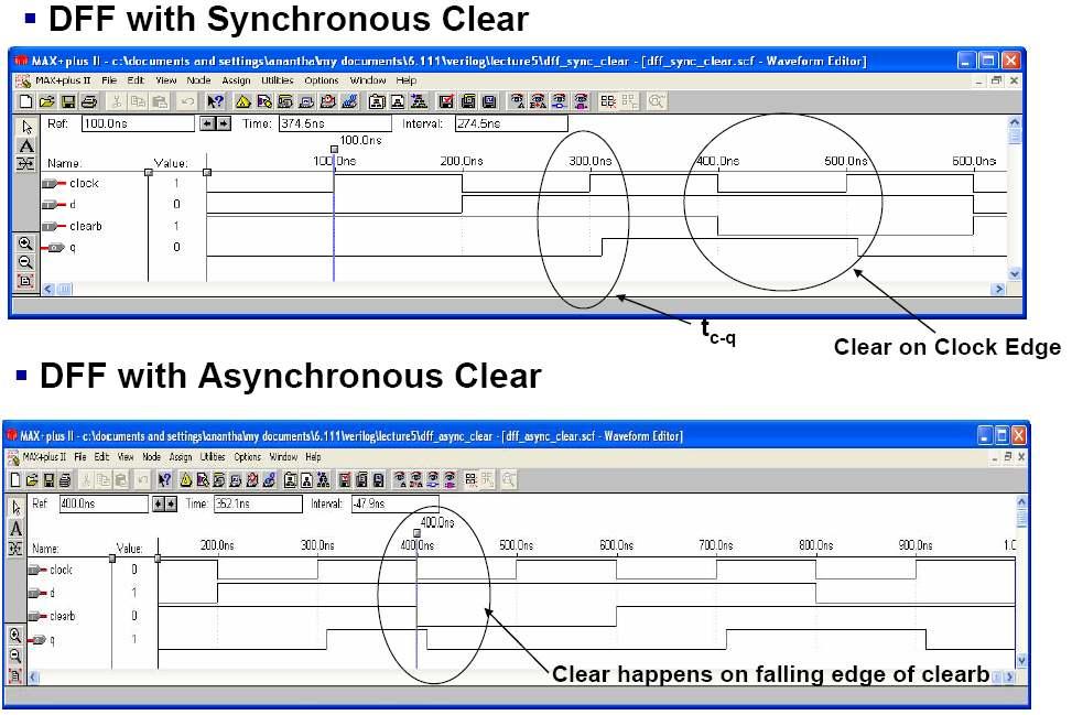
48 Ports n Descriptions ports provide the interface by which a module can communicate with its environment n Types input, output or inout (implicitly all are declared as wire in Verilog) n Port Data Types input or inout ports cannot be of type reg, because reg variables store values input ports should only reflect the changes of external signals they are connected to module DFF (dout,din,clk,resetn); output dout; input din,clk,resetn; reg dout; // As the output of D FF holds value it is declared as reg clk or negedge resetn) if (~resetn) dout<=0; else dout<=din; endmodule 48
49 Port Connection Rules n Ports Inputs Internally, input ports must always be of the type net Externally, the inputs can be connected to a variable which is reg or net Outputs Internally, output ports can be of the type reg or net Externally, the outputs must always be connected to a net Inouts Internally, inout ports must always be of the type net Externally, inout ports must always be connected to a net 49
50 Port Connection Rules (3) n Connections By order By name 50
51 Port Connection Rules: By Order Example module TOP; reg data_in,clock,resetn; wire data_out; // In the following block DFF module is instantiated // and is called DFF_TEST // Signals are connected to ports in order DFF DFF_TEST (data_out,data_in,clock,resetn); <Stimulus> endmodule 51
52 Port Connection Rules: By Name n Connecting ports by name In large designs where the number of ports is great it may seem hard to use the ordered method of port connection Verilog provides the capability to connect external signals to ports by the port names As long as the port name is not changed the order of ports in the port list of a module can be rearranged without changing the port connections in module instantiations DFF DFF_TEST(.din(data_in),.dout(data_out),.resetn(resetn),.clk(clock)); 52
53 Gate Level Implementation of a 4 to 1 MUX in1 w in2 x out in3 y in4 z cntrl1 cntrl2 53
54 Gate Level Implementation of a 4 to 1 MUX : Verilog Description module multiplexor4_1(out, in1, in2, in3, in4, cntrl1, cntrl2); output out; input in1, in2, in3, in4, cntrl1, cntrl2; wire notcntlr1, notcntrl2, w, x, y, z; not (notcntrl1, cntrl1); not (notcntrl2, cntrl2); and (w, in1, notcntrl1, notcntrl2); and (x, in2, notcntrl1, cntrl2); and (y, in3, cntrl1, notcntrl2); and (z, in4, cntrl1, cntrl2); or (out, w, x, y, z); endmodule 54
55 Switch Level Modeling n Behavioral modeling n Data flow modeling n Gate level modeling n Switch level modeling n Others 55
56 Switch-level Primitives n MOS switch nmos, rnmos, pmos, rpmos, cmos, rcmos n Bidirectional pass switch tran, rtran, tranif1, rtranif1, tranif0, rtranif0 n Switch-level net trireg n Power sources pullup, pulldown 56
57 Use of trireg: Example pullup(vdd); trireg (small) #(3,3,10) TriS; trireg (medium) #(6,7,30) TriM; trireg (large) #(15,16,50) TriL; // pass transistor network: tran (TriM, TriS); // left always wins tran (TriM, TriL); // right always wins // NMOS network: rnmos #1 (TriM, TriS, vdd); // input has no effect rnmos #1 (TriS, TriL, vdd); // input controls output rnmos #1 (TriM, TriL, vdd); // connection on output 57
58 Others n The Power of Verilog n Dangers of Verilog n Interconnecting Modules 58

59 The Power of Verilog: n-bit Signals 59
60 The Power of Verilog: Integer Arithmetic 60

61 Dangers of Verilog: Incomplete Specification 61

62 Incomplete Specification Infers Latches 62
63 Avoiding Incomplete Specification Undefined in RHS is not good style, in fact. 63
64 Sensitivity List in Verilog 2001 Style (a or b or c) case({a, b}) 2 b00: d = c; 2 b01: d = ~c; 2 b10: d = {c[0], c[1]}; 2 b11: d = {~c[0], c[1]}; endcase * case({a, b}) 2 b00: d = c; 2 b01: d = ~c; 2 b10: d = {c[0], c[1]}; 2 b11: d = {~c[0], c[1]}; endcase 64

65 Dangers of Verilog : Priority Logic 65

66 Priority Logic 66
")
67 Avoiding (Unintended) Priority Logic 67
68 Interconnecting Modules 68
69 Module Definitions 69

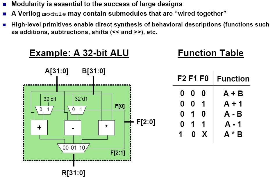
70 Top-Level ALU Declaration 70
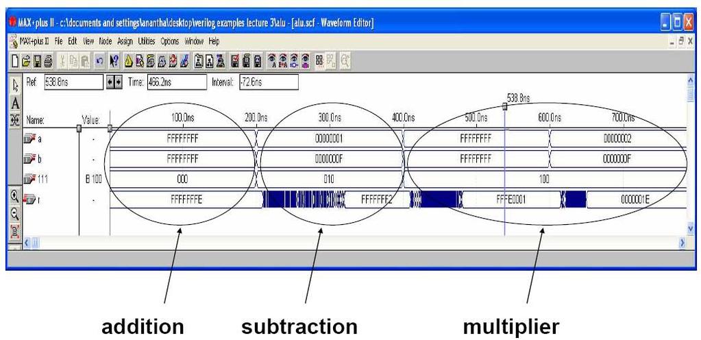
71 Simulation 71
72 More on Module Interconnection 72
Verilog Tutorial (Structure, Test)
") Digital Circuit Design and Language Verilog Tutorial (Structure, Test) Chang, Ik Joon Kyunghee University Hierarchical Design Top-down Design Methodology Bottom-up Design Methodology Module START Example)
Digital Circuit Design and Language Verilog Tutorial (Structure, Test) Chang, Ik Joon Kyunghee University Hierarchical Design Top-down Design Methodology Bottom-up Design Methodology Module START Example)
Programmable Logic Devices Verilog VII CMPE 415
 Synthesis of Combinational Logic In theory, synthesis tools automatically create an optimal gate-level realization of a design from a high level HDL description. In reality, the results depend on the skill
Introduction to Verilog design. Design flow (from the book)
") Introduction to Verilog design Lecture 2 ECE 156A 1 Design flow (from the book) ECE 156A 2 1 Hierarchical Design Chip Modules Cells Primitives A chip contain many modules A module may contain other modules
Introduction to Verilog design Lecture 2 ECE 156A 1 Design flow (from the book) ECE 156A 2 1 Hierarchical Design Chip Modules Cells Primitives A chip contain many modules A module may contain other modules
Introduction to Verilog design. Design flow (from the book) Hierarchical Design. Lecture 2
 Hierarchical Design. Lecture 2") Introduction to Verilog design Lecture 2 ECE 156A 1 Design flow (from the book) ECE 156A 2 Hierarchical Design Chip Modules Cells Primitives A chip contain many modules A module may contain other modules
Introduction to Verilog design Lecture 2 ECE 156A 1 Design flow (from the book) ECE 156A 2 Hierarchical Design Chip Modules Cells Primitives A chip contain many modules A module may contain other modules
Verilog. Like VHDL, Verilog HDL is like a programming language but:
 Verilog Verilog Like VHDL, Verilog HDL is like a programming language but: Statements can execute simultaneously unlike programming e.g. nand(y1,a1,b1); nand(y2,a2,b2); or (out,y1,y2); a1 b1 all statements
Online Verilog Resources
 EECS 427 Discussion 6: Verilog HDL Reading: Many references EECS 427 F08 Discussion 6 1 Online Verilog Resources ASICs the book, Ch. 11: http://www.ge.infn.it/~pratolo/verilog/verilogtutorial.pdf it/ pratolo/verilog/verilogtutorial
EECS 427 Lecture 14: Verilog HDL Reading: Many handouts/references. EECS 427 W07 Lecture 14 1
 EECS 427 Lecture 14: Verilog HDL Reading: Many handouts/references EECS 427 W07 Lecture 14 1 Online Verilog Resources ASICs the book, Ch. 11: http://www.ge.infn.it/~pratolo/verilog/verilogtutorial.pdf
Speaker: Kayting Adviser: Prof. An-Yeu Wu Date: 2009/11/23
 98-1 Under-Graduate Project Synthesis of Combinational Logic Speaker: Kayting Adviser: Prof. An-Yeu Wu Date: 2009/11/23 What is synthesis? Outline Behavior Description for Synthesis Write Efficient HDL
Computer Aided Design Basic Syntax Gate Level Modeling Behavioral Modeling. Verilog
 Verilog Radek Pelánek and Šimon Řeřucha Contents 1 Computer Aided Design 2 Basic Syntax 3 Gate Level Modeling 4 Behavioral Modeling Computer Aided Design Hardware Description Languages (HDL) Verilog C
VERILOG QUICKSTART. Second Edition. A Practical Guide to Simulation and Synthesis in Verilog
 VERILOG QUICKSTART A Practical Guide to Simulation and Synthesis in Verilog Second Edition VERILOG QUICKSTART A Practical Guide to Simulation and Synthesis in Verilog Second Edition James M. Lee SEVA Technologies
Course Topics - Outline
 Course Topics - Outline Lecture 1 - Introduction Lecture 2 - Lexical conventions Lecture 3 - Data types Lecture 4 - Operators Lecture 5 - Behavioral modeling A Lecture 6 Behavioral modeling B Lecture 7
Synthesis of Language Constructs. 5/10/04 & 5/13/04 Hardware Description Languages and Synthesis
 Synthesis of Language Constructs 1 Nets Nets declared to be input or output ports are retained Internal nets may be eliminated due to logic optimization User may force a net to exist trireg, tri0, tri1
The Verilog Language COMS W Prof. Stephen A. Edwards Fall 2002 Columbia University Department of Computer Science
 The Verilog Language COMS W4995-02 Prof. Stephen A. Edwards Fall 2002 Columbia University Department of Computer Science The Verilog Language Originally a modeling language for a very efficient event-driven
OVERVIEW: ============================================================ REPLACE
 OVERVIEW: With mantis 928, formal arguments to properties and sequences are defined to apply to a list of arguments that follow, much like tasks and function arguments. Previously, the type had to be replicated
ECEN 468 Advanced Logic Design
 ECEN 468 Advanced Logic Design Lecture 28: Synthesis of Language Constructs Synthesis of Nets v An explicitly declared net may be eliminated in synthesis v Primary input and output (ports) are always retained
CSE241 VLSI Digital Circuits Winter Recitation 1: RTL Coding in Verilog
 CSE241 VLSI Digital Circuits Winter 2003 Recitation 1: RTL Coding in Verilog CSE241 R1 Verilog.1 Kahng & Cichy, UCSD 2003 Topic Outline Introduction Verilog Background Connections Modules Procedures Structural
CSE140L: Components and Design Techniques for Digital Systems Lab
 CSE140L: Components and Design Techniques for Digital Systems Lab Tajana Simunic Rosing Source: Vahid, Katz, Culler 1 Announcements & Outline Lab 4 due; demo signup times listed on the cse140l site Check
CSE140L: Components and Design
 CSE140L: Components and Design Techniques for Digital Systems Lab Tajana Simunic Rosing Source: Vahid, Katz, Culler 1 Grade distribution: 70% Labs 35% Lab 4 30% Lab 3 20% Lab 2 15% Lab 1 30% Final exam
Under-Graduate Project Logic Design with Behavioral Models
 97-1 1 Under-Graduate Project Logic Design with Behavioral Models Speaker: 吳佳謙 Adviser: Prof. An-Yeu Wu Date: 2008/10/20 ACCESS IC LAB Operation Assignment Outline Blocking and non-blocking Appendix pp.
Why Should I Learn This Language? VLSI HDL. Verilog-2
 Verilog Why Should I Learn This Language? VLSI HDL Verilog-2 Different Levels of Abstraction Algorithmic the function of the system RTL the data flow the control signals the storage element and clock Gate
EEL 4783: HDL in Digital System Design
 EEL 4783: HDL in Digital System Design Lecture 15: Logic Synthesis with Verilog Prof. Mingjie Lin 1 Verilog Synthesis Synthesis vs. Compilation Descriptions mapped to hardware Verilog design patterns for
Synthesizable Verilog
 Synthesizable Verilog Courtesy of Dr. Edwards@Columbia, and Dr. Franzon@NCSU http://csce.uark.edu +1 (479) 575-6043 yrpeng@uark.edu Design Methodology Structure and Function (Behavior) of a Design HDL
Contents. Appendix D Verilog Summary Page 1 of 16
 Appix D Verilog Summary Page 1 of 16 Contents Appix D Verilog Summary... 2 D.1 Basic Language Elements... 2 D.1.1 Keywords... 2 D.1.2 Comments... 2 D.1.3 Identifiers... 2 D.1.4 Numbers and Strings... 3
Chapter 2a: Structural Modeling
 Chapter 2a: Structural Modeling Prof. Ming-Bo Lin Department of Electronic Engineering National Taiwan University of Science and Technology Digital System Designs and Practices Using Verilog HDL and FPGAs
Logic Synthesis. EECS150 - Digital Design Lecture 6 - Synthesis
 Logic Synthesis Verilog and VHDL started out as simulation languages, but quickly people wrote programs to automatically convert Verilog code into low-level circuit descriptions (netlists). EECS150 - Digital
Advanced Digital Design Using FPGA. Dr. Shahrokh Abadi
 Advanced Digital Design Using FPGA Dr. Shahrokh Abadi 1 Venue Computer Lab: Tuesdays 10 12 am (Fixed) Computer Lab: Wednesday 10-12 am (Every other odd weeks) Note: Due to some unpredicted problems with
Synthesis vs. Compilation Descriptions mapped to hardware Verilog design patterns for best synthesis. Spring 2007 Lec #8 -- HW Synthesis 1
 Verilog Synthesis Synthesis vs. Compilation Descriptions mapped to hardware Verilog design patterns for best synthesis Spring 2007 Lec #8 -- HW Synthesis 1 Logic Synthesis Verilog and VHDL started out
P-1/P-105. Samir Palnitkar. Prentice-Hall, Inc. INSTRUCTOR : CHING-LUNG SU.
 : P-1/P-105 Textbook: Verilog HDL 2 nd. Edition Samir Palnitkar Prentice-Hall, Inc. : INSTRUCTOR : CHING-LUNG SU E-mail: kevinsu@yuntech.edu.tw Chapter 7 P-2/P-105 Chapter 7 Behavioral Modeling Outline
Verilog. What is Verilog? VHDL vs. Verilog. Hardware description language: Two major languages. Many EDA tools support HDL-based design
 Verilog What is Verilog? Hardware description language: Are used to describe digital system in text form Used for modeling, simulation, design Two major languages Verilog (IEEE 1364), latest version is
CS6710 Tool Suite. Verilog is the Key Tool
 CS6710 Tool Suite Verilog-XL Behavioral Verilog Your Library Cadence SOC Encounter Synopsys Synthesis Structural Verilog Circuit Layout CSI Verilog-XL AutoRouter Cadence Virtuoso Layout LVS Layout-XL Cadence
UNIT V: SPECIFICATION USING VERILOG HDL
 UNIT V: SPECIFICATION USING VERILOG HDL PART -A (2 Marks) 1. What are identifiers? Identifiers are names of modules, variables and other objects that we can reference in the design. Identifiers consists
Verilog HDL Introduction
 EEE3050 Theory on Computer Architectures (Spring 2017) Prof. Jinkyu Jeong Verilog HDL Introduction 2017.05.14 TA 이규선 (GYUSUN LEE) / 안민우 (MINWOO AHN) Modules The Module Concept Basic design unit Modules
Chap 6 Introduction to HDL (d)
") Design with Verilog Chap 6 Introduction to HDL (d) Credit to: MD Rizal Othman Faculty of Electrical & Electronics Engineering Universiti Malaysia Pahang Ext: 6036 VERILOG HDL Basic Unit A module Module
Design with Verilog Chap 6 Introduction to HDL (d) Credit to: MD Rizal Othman Faculty of Electrical & Electronics Engineering Universiti Malaysia Pahang Ext: 6036 VERILOG HDL Basic Unit A module Module
EECS150 - Digital Design Lecture 10 Logic Synthesis
 EECS150 - Digital Design Lecture 10 Logic Synthesis September 26, 2002 John Wawrzynek Fall 2002 EECS150 Lec10-synthesis Page 1 Logic Synthesis Verilog and VHDL stated out as simulation languages, but quickly
RIZALAFANDE CHE ISMAIL TKT. 3, BLOK A, PPK MIKRO-e KOMPLEKS PENGAJIAN KUKUM. SYNTHESIS OF COMBINATIONAL LOGIC (Chapter 8)
") RIZALAFANDE CHE ISMAIL TKT. 3, BLOK A, PPK MIKRO-e KOMPLEKS PENGAJIAN KUKUM SYNTHESIS OF COMBINATIONAL LOGIC (Chapter 8) HDL-BASED SYNTHESIS Modern ASIC design use HDL together with synthesis tool to create
RIZALAFANDE CHE ISMAIL TKT. 3, BLOK A, PPK MIKRO-e KOMPLEKS PENGAJIAN KUKUM SYNTHESIS OF COMBINATIONAL LOGIC (Chapter 8) HDL-BASED SYNTHESIS Modern ASIC design use HDL together with synthesis tool to create
Graduate Institute of Electronics Engineering, NTU. Lecturer: Chihhao Chao Date:
 Synthesizable Coding of Verilog Lecturer: Date: 2009.03.18 ACCESS IC LAB Outline Basic concepts of logic synthesis Synthesizable Verilog coding subset Verilog coding practices Coding for readability Coding
Verilog Behavioral Modeling
 Verilog Behavioral Modeling Lan-Da Van ( 范倫達 ), Ph. D. Department of Computer Science National Chiao Tung University Taiwan, R.O.C. Spring, 2017 ldvan@cs.nctu.edu.tw http://www.cs.nctu.edu.tw/~ldvan/ Source:
VERILOG QUICKSTART. James M. Lee Cadence Design Systems, Inc. SPRINGER SCIENCE+BUSINESS MEDIA, LLC
 VERILOG QUICKSTART VERILOG QUICKSTART by James M. Lee Cadence Design Systems, Inc. ~. " SPRINGER SCIENCE+BUSINESS MEDIA, LLC ISBN 978-1-4613-7801-3 ISBN 978-1-4615-6113-2 (ebook) DOI 10.1007/978-1-4615-6113-2
EECS150 - Digital Design Lecture 10 Logic Synthesis
 EECS150 - Digital Design Lecture 10 Logic Synthesis February 13, 2003 John Wawrzynek Spring 2003 EECS150 Lec8-synthesis Page 1 Logic Synthesis Verilog and VHDL started out as simulation languages, but
Verilog Design Principles
 16 h7fex // 16-bit value, low order 4 bits unknown 8 bxx001100 // 8-bit value, most significant 2 bits unknown. 8 hzz // 8-bit value, all bits high impedance. Verilog Design Principles ECGR2181 Extra Notes
Introduction To Verilog Design. Chun-Hung Chou
 Introduction To Verilog Design Chun-Hung Chou 1 Outline Typical Design Flow Design Method Lexical Convention Data Type Data Assignment Event Control Conditional Description Register Description Synthesizable
Lecture 15: System Modeling and Verilog
 Lecture 15: System Modeling and Verilog Slides courtesy of Deming Chen Intro. VLSI System Design Outline Outline Modeling Digital Systems Introduction to Verilog HDL Use of Verilog HDL in Synthesis Reading
Lecture 2: Data Types, Modeling Combinational Logic in Verilog HDL. Variables and Logic Value Set. Data Types. Why use an HDL?
 Why use an HDL? Lecture 2: Data Types, Modeling Combinational Logic in Verilog HDL Increase digital design engineer s productivity (from Dataquest) Behavioral HDL RTL HDL Gates Transistors 2K 10K gates/week
Verilog HDL. A Guide to Digital Design and Synthesis. Samir Palnitkar. SunSoft Press A Prentice Hall Title
 Verilog HDL A Guide to Digital Design and Synthesis Samir Palnitkar SunSoft Press A Prentice Hall Title Table of Contents About the Author Foreword Preface Acknowledgments v xxxi xxxiii xxxvii Part 1:
EN2911X: Reconfigurable Computing Topic 02: Hardware Definition Languages
 EN2911X: Reconfigurable Computing Topic 02: Hardware Definition Languages Professor Sherief Reda http://scale.engin.brown.edu School of Engineering Brown University Spring 2014 1 Introduction to Verilog
Verilog Tutorial. Introduction. T. A.: Hsueh-Yi Lin. 2008/3/12 VLSI Digital Signal Processing 2
 Verilog Tutorial T. A.: Hsueh-Yi Lin Introduction 2008/3/12 VLSI Digital Signal Processing 2 Verilog: A common language for industry HDL is a common way for hardware design Verilog VHDL Verilog is widely
Hardware Description Language (HDL)
") Hardware Description Language (HDL) What is the need for Hardware Description Language? Model, Represent, And Simulate Digital Hardware Hardware Concurrency Parallel Activity Flow Semantics for Signal
Hardware Description Language (HDL) What is the need for Hardware Description Language? Model, Represent, And Simulate Digital Hardware Hardware Concurrency Parallel Activity Flow Semantics for Signal
Brief Introduction of Cell-based Design. Ching-Da Chan CIC/DSD
 Brief Introduction of Cell-based Design Ching-Da Chan CIC/DSD 1 Design Abstraction Levels SYSTEM MODULE + GATE CIRCUIT S n+ G DEVICE n+ D 2 Full Custom V.S Cell based Design Full custom design Better patent
Digital System Design Verilog-Part III. Amir Masoud Gharehbaghi
 Digital System Design Verilog-Part III Amir Masoud Gharehbaghi amgh@mehr.sharif.edu Procedural Blocks initial block always block Place in module body Run concurrently with other module constructs Continuous
Graduate Institute of Electronics Engineering, NTU Basic Concept of HDL
 Basic Concept of HDL Lecturer: ( ) Date: 2004.03.05 ACCESS IC LAB Outline Hierarchical Design Methodology Basic Concept of Verilog HDL Switch Level Modeling Gate Level Modeling Simulation & Verification
N-input EX-NOR gate. N-output inverter. N-input NOR gate
 Hardware Description Language HDL Introduction HDL is a hardware description language used to design and document electronic systems. HDL allows designers to design at various levels of abstraction. It
Gate level or structural modeling
 Gate level or structural modeling Prerequisites Functioning of basic logic gates and basic understanding of Verilog coding is required. You are suggested to complete the previous unit before starting this
CS6710 Tool Suite. Verilog is the Key Tool. Verilog as HDL (AHT) Verilog has a Split Personality. Quick Review. Synthesis
 Verilog has a Split Personality. Quick Review. Synthesis") CS6710 Tool Suite Verilog is the Key Tool Verilog-XL Behavioral Verilog Your Library AutoRouter Cadence SOC Encounter Cadence Virtuoso Layout Synopsys Synthesis Circuit Layout CSI LVS Layout-XL Structural
CS6710 Tool Suite Verilog is the Key Tool Verilog-XL Behavioral Verilog Your Library AutoRouter Cadence SOC Encounter Cadence Virtuoso Layout Synopsys Synthesis Circuit Layout CSI LVS Layout-XL Structural
Schematic design. Gate level design. 0 EDA (Electronic Design Assistance) 0 Classical design. 0 Computer based language
 0 Classical design. 0 Computer based language") 1 / 15 2014/11/20 0 EDA (Electronic Design Assistance) 0 Computer based language 0 HDL (Hardware Description Language) 0 Verilog HDL 0 Created by Gateway Design Automation Corp. in 1983 First modern hardware
1 / 15 2014/11/20 0 EDA (Electronic Design Assistance) 0 Computer based language 0 HDL (Hardware Description Language) 0 Verilog HDL 0 Created by Gateway Design Automation Corp. in 1983 First modern hardware
CSE 2021 Computer Organization. The Basics of Logic Design
 CSE 2021 Computer Organization Appendix C The Basics of Logic Design Outline Fundamental Boolean operations Deriving logic expressions from truth tables Boolean Identities Simplifying logic expressions
ECEN 449 Microprocessor System Design. Verilog. Texas A&M University
 ECEN 449 Microprocessor System Design Verilog 1 Objectives of this Lecture Unit Get a feel for the basics of Verilog The focus of this unit will be along two separate but equally relevant axes We will
Course Topics - Outline
 Course Topics - Outline Lecture 1 - Introduction Lecture 2 - Lexical conventions Lecture 3 - Data types Lecture 4 - Operators Lecture 5 - Behavioral modeling A Lecture 6 Behavioral modeling B Lecture 7
This Lecture. Some components (useful for the homework) Verilog HDL (will continue next lecture)
 Verilog HDL (will continue next lecture)") Last Lecture The basic component of a digital circuit is the MOS transistor Transistor have instrinsic resistance and capacitance, so voltage values in the circuit take some time to change ( delay ) There
Last Lecture The basic component of a digital circuit is the MOS transistor Transistor have instrinsic resistance and capacitance, so voltage values in the circuit take some time to change ( delay ) There
Chapter 2 Using Hardware Description Language Verilog. Overview
 Chapter 2 Using Hardware Description Language Verilog CSE4210 Winter 2012 Mokhtar Aboelaze based on slides by Dr. Shoab A. Khan Overview Algorithm development isa usually done in MATLAB, C, or C++ Code
Introduction to Verilog/System Verilog
 NTUEE DCLAB Feb. 27, 2018 Introduction to Verilog/System Verilog Presenter: Yao-Pin Wang 王耀斌 Advisor: Prof. Chia-Hsiang Yang 楊家驤 Dept. of Electrical Engineering, NTU National Taiwan University What is
VLSI Design 13. Introduction to Verilog
 Last module: Sequential circuit design Design styles This module Synthesis Brief introduction to Verilog Synthesis in the Design Flow Designer Tasks Tools Architect Logic Designer Circuit Designer Define
a, b sum module add32 sum vector bus sum[31:0] sum[0] sum[31]. sum[7:0] sum sum overflow module add32_carry assign
![a, b sum module add32 sum vector bus sum[31:0] sum[0] sum[31]. sum[7:0] sum sum overflow module add32_carry assign](/thumbs/91/106466219.jpg "a, b sum module add32 sum vector bus sum[31:0] sum[0] sum[31]. sum[7:0] sum sum overflow module add32_carry assign") I hope you have completed Part 1 of the Experiment. This lecture leads you to Part 2 of the experiment and hopefully helps you with your progress to Part 2. It covers a number of topics: 1. How do we specify
I hope you have completed Part 1 of the Experiment. This lecture leads you to Part 2 of the experiment and hopefully helps you with your progress to Part 2. It covers a number of topics: 1. How do we specify
14. Introducton to Verilog
 14. Introducton to Verilog Jacob Abraham Department of Electrical and Computer Engineering The University of Texas at Austin VLSI Design Fall 2017 October 23, 2017 ECE Department, University of Texas at
Veriolog Overview. CS/EE 3710 Fall 2010
 Veriolog Overview CS/EE 3710 Fall 2010 Hardware Description Languages HDL Designed to be an alternative to schematics for describing hardware systems Two main survivors VHDL Commissioned by DOD Based on
Verilog Design Principles
 16 h7fex // 16-bit value, low order 4 bits unknown 8 bxx001100 // 8-bit value, most significant 2 bits unknown. 8 hzz // 8-bit value, all bits high impedance. Verilog Design Principles ECGR2181 Extra Notes
EN164: Design of Computing Systems Lecture 06: Lab Foundations / Verilog 2
 EN164: Design of Computing Systems Lecture 06: Lab Foundations / Verilog 2 Professor Sherief Reda http://scaleenginbrownedu Electrical Sciences and Computer Engineering School of Engineering Brown University
FPGA Design Challenge :Techkriti 14 Digital Design using Verilog Part 1
 FPGA Design Challenge :Techkriti 14 Digital Design using Verilog Part 1 Anurag Dwivedi Digital Design : Bottom Up Approach Basic Block - Gates Digital Design : Bottom Up Approach Gates -> Flip Flops Digital
Appendix A GATE-LEVEL DETAILS
 Appendix A GATE-LEVEL DETAILS Chapters 2 and 3 1:riefly introduced the built-in primitives. This appendix will 1:riefly describe each of the built-in primitives and the options when instantiating them.
Combinational Logic II
 Combinational Logic II Ranga Rodrigo July 26, 2009 1 Binary Adder-Subtractor Digital computers perform variety of information processing tasks. Among the functions encountered are the various arithmetic
Department of Computer Science and Electrical Engineering. Intro to Verilog II
 Department of Computer Science and Electrical Engineering Intro to Verilog II http://6004.csail.mit.edu/6.371/handouts/l0{2,3,4}.pdf http://www.asic-world.com/verilog/ http://www.verilogtutorial.info/
register:a group of binary cells suitable for holding binary information flip-flops + gates
 9 차시 1 Ch. 6 Registers and Counters 6.1 Registers register:a group of binary cells suitable for holding binary information flip-flops + gates control when and how new information is transferred into the
Advanced Digital Design with the Verilog HDL
 Copyright 2001, 2003 MD Ciletti 1 Advanced Digital Design with the Verilog HDL M. D. Ciletti Department of Electrical and Computer Engineering University of Colorado Colorado Springs, Colorado ciletti@vlsic.uccs.edu
ECE 2300 Digital Logic & Computer Organization. More Sequential Logic Verilog
 ECE 2300 Digital Logic & Computer Organization Spring 2018 More Sequential Logic Verilog Lecture 7: 1 Announcements HW3 will be posted tonight Prelim 1 Thursday March 1, in class Coverage: Lectures 1~7
Synthesis of Combinational and Sequential Circuits with Verilog
 Synthesis of Combinational and Sequential Circuits with Verilog What is Verilog? Hardware description language: Are used to describe digital system in text form Used for modeling, simulation, design Two
Design Using Verilog
 EGC220 Design Using Verilog Baback Izadi Division of Engineering Programs bai@engr.newpaltz.edu Basic Verilog Lexical Convention Lexical convention are close to C++. Comment // to the of the line. /* to
CSE140L: Components and Design Techniques for Digital Systems Lab. Verilog HDL. Instructor: Mohsen Imani UC San Diego. Source: Eric Crabill, Xilinx
 CSE140L: Components and Design Techniques for Digital Systems Lab Verilog HDL Instructor: Mohsen Imani UC San Diego Source: Eric Crabill, Xilinx 1 Hardware description languages Used to describe & model
A Tutorial Introduction 1
 Preface From the Old to the New Acknowledgments xv xvii xxi 1 Verilog A Tutorial Introduction 1 Getting Started A Structural Description Simulating the binarytoeseg Driver Creating Ports For the Module
ECEN 449 Microprocessor System Design. Verilog. Texas A&M University
 ECEN 449 Microprocessor System Design Verilog 1 Objectives of this Lecture Unit Get a feel for the basics of Verilog The focus of this unit will be along two separate e but equally relevant ev axes We
The Verilog Hardware Description Language
 Donald Thomas Philip Moorby The Verilog Hardware Description Language Fifth Edition 4y Spri nnger Preface From the Old to the New Acknowledgments xv xvii xxi 1 Verilog A Tutorial Introduction Getting Started
ENGN1640: Design of Computing Systems Topic 02: Design/Lab Foundations
 ENGN1640: Design of Computing Systems Topic 02: Design/Lab Foundations Professor Sherief Reda http://scale.engin.brown.edu School of Engineering Brown University Spring 2017 1 Topics 1. Programmable logic
Digital Design (VIMIAA01) Introduction to the Verilog HDL
 Introduction to the Verilog HDL") BUDAPEST UNIVERSITY OF TECHNOLOGY AND ECONOMICS FACULTY OF ELECTRICAL ENGINEERING AND INFORMATICS DEPARTMENT OF MEASUREMENT AND INFORMATION SYSTEMS Digital Design (VIMIAA01) Introduction to the Verilog
BUDAPEST UNIVERSITY OF TECHNOLOGY AND ECONOMICS FACULTY OF ELECTRICAL ENGINEERING AND INFORMATICS DEPARTMENT OF MEASUREMENT AND INFORMATION SYSTEMS Digital Design (VIMIAA01) Introduction to the Verilog
Digital Design with SystemVerilog
 Digital Design with SystemVerilog Prof. Stephen A. Edwards Columbia University Spring 25 Synchronous Digital Design Combinational Logic Sequential Logic Summary of Modeling Styles Testbenches Why HDLs?
Verilog introduction. Embedded and Ambient Systems Lab
 Verilog introduction Embedded and Ambient Systems Lab Purpose of HDL languages Modeling hardware behavior Large part of these languages can only be used for simulation, not for hardware generation (synthesis)
Introduction to Verilog
 Introduction to Verilog Course Objectives Learn the basic constructs of Verilog Learn the modeling structure of Verilog Learn the concept of delays and their effects in simulation Course Outline Verilog
Date Performed: Marks Obtained: /10. Group Members (ID):. Experiment # 11. Introduction to Verilog II Sequential Circuits
:. Experiment # 11. Introduction to Verilog II Sequential Circuits") Name: Instructor: Engr. Date Performed: Marks Obtained: /10 Group Members (ID):. Checked By: Date: Experiment # 11 Introduction to Verilog II Sequential Circuits OBJECTIVES: To understand the concepts
Name: Instructor: Engr. Date Performed: Marks Obtained: /10 Group Members (ID):. Checked By: Date: Experiment # 11 Introduction to Verilog II Sequential Circuits OBJECTIVES: To understand the concepts
ENGN1640: Design of Computing Systems Topic 02: Design/Lab Foundations
 ENGN1640: Design of Computing Systems Topic 02: Design/Lab Foundations Professor Sherief Reda http://scale.engin.brown.edu School of Engineering Brown University Spring 2016 1 Topics 1. Programmable logic
Actel HDL Coding. Style Guide
 Actel HDL Coding Style Guide Actel Corporation, Mountain View, CA 94043 2003 Actel Corporation. All rights reserved. Printed in the United States of America Part Number: 5029105-6/05.04 Release: May 2004
Chap 3. Modeling structure & basic concept of Verilog HDL
 Chap 3. Modeling structure & basic concept of Verilog HDL Fall semester, 2016 Prof. Jaeseok Kim School of Electrical & Electronics Eng. Yonsei university jaekim@yonsei.ac.kr Digital System Design 3-1 Chapter
In this lecture, we will go beyond the basic Verilog syntax and examine how flipflops and other clocked circuits are specified.
 1 In this lecture, we will go beyond the basic Verilog syntax and examine how flipflops and other clocked circuits are specified. I will also introduce the idea of a testbench as part of a design specification.
Verilog Fundamentals. Shubham Singh. Junior Undergrad. Electrical Engineering
 Verilog Fundamentals Shubham Singh Junior Undergrad. Electrical Engineering VERILOG FUNDAMENTALS HDLs HISTORY HOW FPGA & VERILOG ARE RELATED CODING IN VERILOG HDLs HISTORY HDL HARDWARE DESCRIPTION LANGUAGE
FPGA: FIELD PROGRAMMABLE GATE ARRAY Verilog: a hardware description language. Reference: [1]
![FPGA: FIELD PROGRAMMABLE GATE ARRAY Verilog: a hardware description language. Reference: [1]](/thumbs/80/81661285.jpg "FPGA: FIELD PROGRAMMABLE GATE ARRAY Verilog: a hardware description language. Reference: [1]") FPGA: FIELD PROGRAMMABLE GATE ARRAY Verilog: a hardware description language Reference: [] FIELD PROGRAMMABLE GATE ARRAY FPGA is a hardware logic device that is programmable Logic functions may be programmed
FPGA: FIELD PROGRAMMABLE GATE ARRAY Verilog: a hardware description language Reference: [] FIELD PROGRAMMABLE GATE ARRAY FPGA is a hardware logic device that is programmable Logic functions may be programmed
A Verilog Primer. An Overview of Verilog for Digital Design and Simulation
 A Verilog Primer An Overview of Verilog for Digital Design and Simulation John Wright Vighnesh Iyer Department of Electrical Engineering and Computer Sciences College of Engineering, University of California,
ES611 FPGA Based System Design. Behavioral Model
 ES611 FPGA Based System Design Behavioral Model Structural procedures Two statements Initial always initial they execute only once always they execute for ever (until simulation finishes) initial block
Verilog for Synthesis Ing. Pullini Antonio
 Verilog for Synthesis Ing. Pullini Antonio antonio.pullini@epfl.ch Outline Introduction to Verilog HDL Describing combinational logic Inference of basic combinational blocks Describing sequential circuits
Contents of Verilog Reference Guide
 Contents of Verilog Reference Guide Contents of Verilog Reference Guide 1 Always Procedural Block 3 Arithmetic Operators 5 Array 7 Bit-Select 9 Bit-wise Operators 10 Block Statement 12 Blocking Assignment
ECEN 468 Advanced Logic Design
 ECEN 468 Advanced Logic Design Lecture 26: Verilog Operators ECEN 468 Lecture 26 Operators Operator Number of Operands Result Arithmetic 2 Binary word Bitwise 2 Binary word Reduction 1 Bit Logical 2 Boolean
Introduction to Verilog
 Introduction to Verilog Synthesis and HDLs Verilog: The Module Continuous (Dataflow) Assignment Gate Level Description Procedural Assignment with always Verilog Registers Mix-and-Match Assignments The
The Verilog Golden Reference Guide
 The Verilog Golden Reference Guide DOULOS Version 1.0, August 1996 Copyright 1996, Doulos, All Rights Reserved. No part of this publication may be reproduced, stored in a retrieval system, or transmitted,
Actel HDL Coding. Style Guide
 Actel HDL Coding Style Guide Actel Corporation, Mountain View, CA 94043 2006 Actel Corporation. All rights reserved. Printed in the United States of America Part Number: 5029105-7 Release: November 2006
430 Index. D flip-flop, from nands, 189, 191, 192 D flip-flop, verilog, 37
 Index *, in event control, 46 -> (event trigger), 177 $display, 34, 146, 165 $display, example, 44 $finish, 11, 165, 195, 196 $fullskew timing check, 297 $hold timing check, 298 $monitor, 34, 174 $nochange