FPGA VHDL Design Flow AES128 Implementation
|
|
|
- Stephen Stokes
- 5 years ago
- Views:
Transcription


1 Sakinder Ali
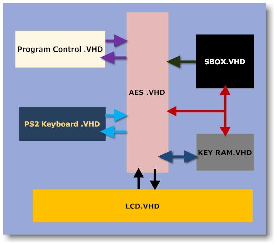
2 FPGA VHDL Design Flow AES128 Implementation

 A X INV AND LUT X B X X X X X Out C X INV OR LUT X X X X X X X LUT LUT LUT The interconnect switches")
3 Field Programmable Gate Array Basic idea: two-dimensional array of logic blocks and flip-flops with a means for the user to configure: 1. The interconnection between the logic blocks, 2. The function of each block. The FPGA LUTs are configured to implement Gates A B C Empty Look Up Tables Adding More Functionality DFF next to a 4-Input LUT to form a "Configurable Logic Block" (CLB) A X INV AND LUT X B X X X X X Out C X INV OR LUT X X X X X X X LUT LUT LUT The interconnect switches are then programmed to implement the net connections X The basic FPGA functional unit: CLB


4 1987: 9,000 gates, Xilinx 1992: 600,000, Naval Surface Warfare Department Early 2000s: Millions 1985: First commercial FPGA technology invented by Xilinx 1987: $14 million ~1993: >$385 million 2005: $1.9 billion 2010 estimates: $2.75 billion


5 NASA/Lockheed X-33 Launch Vehicle The SpaceWire communications system is driven by low-power chips. VMC: The Venus Monitoring Camera is a wide-angle, multi-channel CCD. The camera includes an FPGA to pre-process image data, reducing the amount transmitted to Earth FPGA used to modify the control algorithm to improve testing, explore shutter issues, and further NASA MEMS microshutter array development. Over the last decade, the company's FPGAs have been onboard more than 100 launches and flown on over 300 satellites and spacecraft, including GPS, Mars Reconnaissance Orbiter, and the Mars Explorer Rovers 1 and 2 (Spirit and Opportunity).
 DATA FRAME GENERATOR FRAME SONET TRANSCEIVER (Up to 77.76 MHz) SONET FPGA BLOCK 1:8 Demuxes (Up to 437.")
 3.5 GHz 437.5 MHz 72.")
 INPUTS OUTPUTS 32 BIT ( WORD ) Serial Data at xxx GHz BIT ALLIGNER BIT ALLIGNER SONET FRAME 48 BIT CHANNEL-0 CHANNEL-3 CHANNEL 11 CHANNEL-7")
6 8-Bit Parallel Input (Up to 3.5GHz) 8:48 Deserialize Bit Ordering FIFO (Up to MHz) ADC CHANNEL Bit Allinger Packetizer (Up to MHz) DATA FRAME GENERATOR FRAME SONET TRANSCEIVER (Up to MHz) SONET FPGA BLOCK 1:8 Demuxes (Up to MHz) 2 CHANNELS OF 8-BITS WIDE 2 CHANNELS OF 48-BITS WIDE 2 CHANNELS OF 48-BITS WIDE 2 CHANNELS OF 48-BITS WIDE 8 CHANNELS OF 48-BITS WIDE 12 CHANNELS OF 32-BITS WIDE 12 CHANNELS OF 32-BITS WIDE 3 CHANNELS OF 32-BITS WIDE 12 CHANNELS OF 32-BITS WIDE (Up to GHz) 3.5 GHz MHz MHz MHz GHz Color Code Input 0 Input 1 Input 2 Input 3 Input 4 Input 5 Input 6 Input 7 Serial Data at xxx GHz Time (0.xxx ns) INPUTS OUTPUTS 32 BIT ( WORD ) Serial Data at xxx GHz BIT ALLIGNER BIT ALLIGNER SONET FRAME 48 BIT CHANNEL-0 CHANNEL-3 CHANNEL 11 CHANNEL-7 CHANNEL-1 CHANNEL-2 CHANNEL-9 CHANNEL-4 CHANNEL-5 CHANNEL-8 CHANNEL-6 CHANNEL-10

7 Virtex-7-HT Virtex-6 Virtex-5 Virtex-4 Virtex-II Pro Spartan-6 Extended Spartan-3A Spartan-3E Spartan-3 28Gbps Serial Transceiver Technology Xilinx Virtex-7 HT FPGA Highlights Enables communication equipment vendors to develop the integrated, high- bandwidth-efficient. Built with four to sixteen 28Gbps transceivers complying with OIF CEI-28G (Optical Internetworking Forum s Common Electrical I/O). Up to seventy-two 13.1Gbps transceivers Up to 2.8Tbps full duplex throughput Features Artix-7 Kintex-7 Virtex-7 Spartan-6 Virtex-6 Logic Cells 352, ,000 2,000, , ,000 BlockRAM 19Mb 34Mb 85Mb 4.8Mb 38Mb DSP Slices 1,040 1,920 5, ,016 DSP Performance (symmetric FIR) 1,129GMACS 2,450GMACS 6,737GMACS 140GMACS 2,419GMACS Transceiver Count Transceiver Speed 6.6Gb/s 12.5Gb/s 28.05Gb/s 3.125Gb/s 11.18Gb/s Total Transceiver Bandwidth (full duplex) 211Gb/s 800Gb/s 2,784Gb/s 50Gb/s 536Gb/s Memory Interface (DDR3) 1,066Mb/s 1,866Mb/s 1,866Mb/s 800Mb/s 1,066Mb/s PCI Express Interface Gen2x4 Gen2x8 Gen3x8 Gen1x1 Gen2x8 Agile Mixed Signal (AMS)/XADC Yes Yes Yes Yes Configuration AES Yes Yes Yes Yes Yes I/O Pins , ,200 The company claims it is the fastest product rollout of next generation programmable logic devices built with 28nm technology.


8 ~$15,000 The technology leadership continues with the transceivers in 28-nm Stratix V FPGAs. Providing up to over 930 Gbps of transceiver bandwidth, Stratix V FPGAs deliver the highest system bandwidth at the lowest power consumption for a wide range of applications and protocols. ~@200 -$500
9 One time programmable Fuses (destroy internal links with current) Anti-fuses (grow internal links) Reprogrammable EPROM EEPROM Flash SRAM - volatile
10 Programmable Function Fusible Link Technology
 and once blown, cannot be undone. 0 (i), the no connection exists between the two metal layers.")
11 Antifuse based configuration uses a two terminal device that is electrically programmed to change from an electrical open circuit to an electrical short circuit. The operation is the inverse to that of the fuse. This is a one-time process (i.e., permanent) and once blown, cannot be undone. 0 (i), the no connection exists between the two metal layers. Once programmed, a low-resistance link (ii) exists between the metal layers and connects them together. Disadvantages Not reprogrammable; links made are permanent Advantages Small size Relatively low series resistance Low parasitic capacitance 1


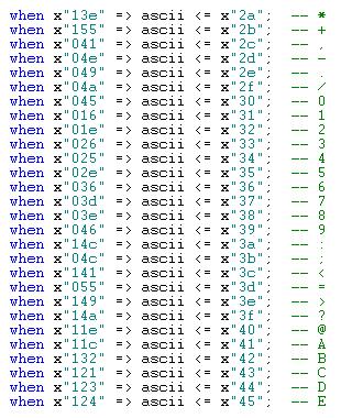
12 Bit Line Bit Line Encryption/Decryption system used by Xilinx to protect the configuration of Virtex-II devices. Word Line - - Control Gate Oxide Layer Floating Gate 1 Drain Word Line Drain Source Control Gate Oxide Layer Floating Gate Source 0 Xilinx CAD software tool encrypts the bitstream using the powerful Triple Data Encryption (DES) algorithm before downloading the configuration inside the FPGA. Triple DES is the standard used by many governments for safe communication and by banks around the world for money transfers. This algorithm uses three 56-bits public keys. The designer can use random keys or choose their own-keys.


13 Configuration data in Configuration data out Disadvantages Volatile External Permanent Memory Required Large Area Required Advantages = I/O pin/pad = SRAM cell Reprogrammable, easily and quickly Requires only standard integrated circuit process technology (as opposed to Antifuse) SRAM-based FPGAs are non-volatile devices. Upon power up, They are required to be programmed from an external source. Most FPGA vendors do not publish the definition of the bit-stream. It is therefore very difficult to reverse engineer a design from a configuration bit-stream.
14 Level 0 (Zero) No special security features added to the system. Level 1 (Low) Some security features in place. Level 2 (Medium Low) More expensive tools are required, as well as specialized knowledge. Level 3 (Medium ) Special tools and equipment are required, as well as some special skills and knowledge. The attack may become time-consuming but will eventually be successful. Level 4 (Medium High) Equipment is available but is expensive to buy and operate. Level 5 (High) All known attacks have been unsuccessful
 Flip-Flops")

15 Basic Components LUT (look-up-table) Flip-Flops Multiplexers I/O Blocks Programmable switching matrices Interconnect Clocks


16 Create a circuit design Graphic circuit tool Verilog VHDL AHDL Vendor Tools
17 VHDL: VHSIC Hardware Description Language VHSIC: Very High Speed Integrated Circuit Developed originally by DARPA for specifying digital systems International IEEE standard (IEEE ) Practical benefits: A mechanism for digital design and reusable design documentation Model interoperability among vendors Third party vendor support Design re-use.

18 It allows the behavior of the required system to be described (modeled) and verified (simulated) before synthesis tools translate the design into real hardware (gates and wires). Allows the description of a concurrent system. VHDL is a dataflow language, unlike procedural computing languages such as BASIC, C, and assembly code, which all run sequentially, one instruction at a time. VHDL project is multipurpose. Being created once, a calculation block can be used in many other projects. However, many formational and functional block parameters can be tuned (capacity parameters, memory size, element base, block composition and interconnection structure). VHDL project is portable. Being created for one element base, a computing device project can be ported on another element base, for example VLSI with various technologies.


19 Interfaces Behavior Structure Test Benches Analysis, elaboration, simulation Synthesis


20 entity name port names port mode (direction) port type punctuation reserved words
21


22
23 Design Entry/RTL Coding - Behavioral or Structural Description of Design RTL Simulation - Functional Simulation - Verify Logic Model & Data Flow (No Timing Delays) Synthesis - Translate Design into Device Specific Primitives - Optimization to Meet Required Area & Performance Constraints Place & Route - Map Primitives to Specific Locations inside Target Technology with Reference to Area & Performance Constraints - Specify Routing Resources to Be Used


24 t clk Timing Analysis - Verify Performance Specifications Were Met - Static Timing Analysis Gate Level Simulation - Timing Simulation - Verify Design Will Work in Target Technology PC Board Simulation & Test - Simulate Board Design - Program & Test Device on Board


25 Logic analysis system provides high-performance, system-level debugging of digital designs. Track down cross domain analog and digital problems by time-correlating logic analysis systems.

26 Advance FPGA design flow Typical FPGA design flow
, for a total throughput of 15 billion")
27 High performance at densities of up to 4 million equivalent system gates and 840 user I/Os for space-based applications. The RTAX-DSP family features up to 120 mathblocks, each capable of operating at 125 MHz over the full military temperature range (- 55 C to 125 C), for a total throughput of 15 billion multiply/accumulates per second (15 GMACS). Key Features Highly reliable, nonvolatile antifuse technology 250,000 to 500,000 ASIC gates (2 to 4 million system gates) Up to 120 DSP mathblocks with 125 MHz 18 bit x 18 bit multiply-accumulate Up to 540 kbits of embedded memory with optional EDAC protection Up to 840 user-programmable I/Os
28 Interfaces to the system (data, clock, control, and status) including width (serial or parallel) Functional blocks in system Interfaces between blocks including data width Data rates into the system and between blocks (data rates are tied to data widths) Clock domains into system and between blocks Memory (size, speed, and width) Standards/specs Timing diagrams (setup, hold, latency tolerance) Schedule.
29 The FPGA is one of the most popular logic circuit components and has revolutionized the way digital systems are designed. Some FPGA advantages include: Low-cost Fast-turnaround prototype implementation Supported by CAD/EDA tools High density High speed Programmable and versatile Flexible Reusable Large amounts of logic gates, registers, RAM and routing resources Quick time-to-market SRAM FPGA provide the benefits of custom CMOS
30


31
32

33


34 Current State Next State
35
36
37 Current State Next State

38
39
40

41
Basic FPGA Architectures. Actel FPGAs. PLD Technologies: Antifuse. 3 Digital Systems Implementation Programmable Logic Devices
 3 Digital Systems Implementation Programmable Logic Devices Basic FPGA Architectures Why Programmable Logic Devices (PLDs)? Low cost, low risk way of implementing digital circuits as application specific
FPGA. Logic Block. Plessey FPGA: basic building block here is 2-input NAND gate which is connected to each other to implement desired function.
 FPGA Logic block of an FPGA can be configured in such a way that it can provide functionality as simple as that of transistor or as complex as that of a microprocessor. It can used to implement different
Field Programmable Gate Array (FPGA)
") Field Programmable Gate Array (FPGA) Lecturer: Krébesz, Tamas 1 FPGA in general Reprogrammable Si chip Invented in 1985 by Ross Freeman (Xilinx inc.) Combines the advantages of ASIC and uc-based systems
Field Programmable Gate Array (FPGA) Lecturer: Krébesz, Tamas 1 FPGA in general Reprogrammable Si chip Invented in 1985 by Ross Freeman (Xilinx inc.) Combines the advantages of ASIC and uc-based systems
INTRODUCTION TO FPGA ARCHITECTURE
 3/3/25 INTRODUCTION TO FPGA ARCHITECTURE DIGITAL LOGIC DESIGN (BASIC TECHNIQUES) a b a y 2input Black Box y b Functional Schematic a b y a b y a b y 2 Truth Table (AND) Truth Table (OR) Truth Table (XOR)
EITF35: Introduction to Structured VLSI Design
 EITF35: Introduction to Structured VLSI Design Introduction to FPGA design Rakesh Gangarajaiah Rakesh.gangarajaiah@eit.lth.se Slides from Chenxin Zhang and Steffan Malkowsky WWW.FPGA What is FPGA? Field
EE219A Spring 2008 Special Topics in Circuits and Signal Processing. Lecture 9. FPGA Architecture. Ranier Yap, Mohamed Ali.
 EE219A Spring 2008 Special Topics in Circuits and Signal Processing Lecture 9 FPGA Architecture Ranier Yap, Mohamed Ali Annoucements Homework 2 posted Due Wed, May 7 Now is the time to turn-in your Hw
FYSE420 DIGITAL ELECTRONICS. Lecture 7
 FYSE420 DIGITAL ELECTRONICS Lecture 7 1 [1] [2] [3] DIGITAL LOGIC CIRCUIT ANALYSIS & DESIGN Nelson, Nagle, Irvin, Carrol ISBN 0-13-463894-8 DIGITAL DESIGN Morris Mano Fourth edition ISBN 0-13-198924-3
Digital Integrated Circuits
 Digital Integrated Circuits Lecture 9 Jaeyong Chung Robust Systems Laboratory Incheon National University DIGITAL DESIGN FLOW Chung EPC6055 2 FPGA vs. ASIC FPGA (A programmable Logic Device) Faster time-to-market
FPGA for Complex System Implementation. National Chiao Tung University Chun-Jen Tsai 04/14/2011
 FPGA for Complex System Implementation National Chiao Tung University Chun-Jen Tsai 04/14/2011 About FPGA FPGA was invented by Ross Freeman in 1989 SRAM-based FPGA properties Standard parts Allowing multi-level
FPGA Programming Technology
 FPGA Programming Technology Static RAM: This Xilinx SRAM configuration cell is constructed from two cross-coupled inverters and uses a standard CMOS process. The configuration cell drives the gates of
LSN 6 Programmable Logic Devices
 LSN 6 Programmable Logic Devices Department of Engineering Technology LSN 6 What Are PLDs? Functionless devices in base form Require programming to operate The logic function of the device is programmed
ECE 636. Reconfigurable Computing. Lecture 2. Field Programmable Gate Arrays I
 ECE 636 Reconfigurable Computing Lecture 2 Field Programmable Gate Arrays I Overview Anti-fuse and EEPROM-based devices Contemporary SRAM devices - Wiring - Embedded New trends - Single-driver wiring -
Spiral 2-8. Cell Layout
 2-8.1 Spiral 2-8 Cell Layout 2-8.2 Learning Outcomes I understand how a digital circuit is composed of layers of materials forming transistors and wires I understand how each layer is expressed as geometric
VHX - Xilinx - FPGA Programming in VHDL
 Training Xilinx - FPGA Programming in VHDL: This course explains how to design with VHDL on Xilinx FPGAs using ISE Design Suite - Programming: Logique Programmable VHX - Xilinx - FPGA Programming in VHDL
PLAs & PALs. Programmable Logic Devices (PLDs) PLAs and PALs
 PLAs and PALs") PLAs & PALs Programmable Logic Devices (PLDs) PLAs and PALs PLAs&PALs By the late 1970s, standard logic devices were all the rage, and printed circuit boards were loaded with them. To offer the ultimate
PLAs & PALs Programmable Logic Devices (PLDs) PLAs and PALs PLAs&PALs By the late 1970s, standard logic devices were all the rage, and printed circuit boards were loaded with them. To offer the ultimate
Field Programmable Gate Array (FPGA) Devices
 Devices") Field Programmable Gate Array (FPGA) Devices 1 Contents Altera FPGAs and CPLDs CPLDs FPGAs with embedded processors ACEX FPGAs Cyclone I,II FPGAs APEX FPGAs Stratix FPGAs Stratix II,III FPGAs Xilinx FPGAs
Field Programmable Gate Array (FPGA) Devices 1 Contents Altera FPGAs and CPLDs CPLDs FPGAs with embedded processors ACEX FPGAs Cyclone I,II FPGAs APEX FPGAs Stratix FPGAs Stratix II,III FPGAs Xilinx FPGAs
Programmable Logic Devices UNIT II DIGITAL SYSTEM DESIGN
 Programmable Logic Devices UNIT II DIGITAL SYSTEM DESIGN 2 3 4 5 6 7 8 9 2 3 4 5 6 7 8 9 2 Implementation in Sequential Logic 2 PAL Logic Implementation Design Example: BCD to Gray Code Converter A B
Chapter 5: ASICs Vs. PLDs
 Chapter 5: ASICs Vs. PLDs 5.1 Introduction A general definition of the term Application Specific Integrated Circuit (ASIC) is virtually every type of chip that is designed to perform a dedicated task.
Today. Comments about assignment Max 1/T (skew = 0) Max clock skew? Comments about assignment 3 ASICs and Programmable logic Others courses
 Max clock skew? Comments about assignment 3 ASICs and Programmable logic Others courses") Today Comments about assignment 3-43 Comments about assignment 3 ASICs and Programmable logic Others courses octor Per should show up in the end of the lecture Mealy machines can not be coded in a single
Today Comments about assignment 3-43 Comments about assignment 3 ASICs and Programmable logic Others courses octor Per should show up in the end of the lecture Mealy machines can not be coded in a single
EECS150 - Digital Design Lecture 6 - Field Programmable Gate Arrays (FPGAs)
") EECS150 - Digital Design Lecture 6 - Field Programmable Gate Arrays (FPGAs) September 12, 2002 John Wawrzynek Fall 2002 EECS150 - Lec06-FPGA Page 1 Outline What are FPGAs? Why use FPGAs (a short history
EECS150 - Digital Design Lecture 6 - Field Programmable Gate Arrays (FPGAs) September 12, 2002 John Wawrzynek Fall 2002 EECS150 - Lec06-FPGA Page 1 Outline What are FPGAs? Why use FPGAs (a short history
Outline. EECS150 - Digital Design Lecture 6 - Field Programmable Gate Arrays (FPGAs) FPGA Overview. Why FPGAs?
 FPGA Overview. Why FPGAs?") EECS150 - Digital Design Lecture 6 - Field Programmable Gate Arrays (FPGAs) September 12, 2002 John Wawrzynek Outline What are FPGAs? Why use FPGAs (a short history lesson). FPGA variations Internal logic
EECS150 - Digital Design Lecture 6 - Field Programmable Gate Arrays (FPGAs) September 12, 2002 John Wawrzynek Outline What are FPGAs? Why use FPGAs (a short history lesson). FPGA variations Internal logic
Field Program mable Gate Arrays
 Field Program mable Gate Arrays M andakini Patil E H E P g r o u p D H E P T I F R SERC school NISER, Bhubaneshwar Nov 7-27 2017 Outline Digital electronics Short history of programmable logic devices
Zynq-7000 All Programmable SoC Product Overview
 Zynq-7000 All Programmable SoC Product Overview The SW, HW and IO Programmable Platform August 2012 Copyright 2012 2009 Xilinx Introducing the Zynq -7000 All Programmable SoC Breakthrough Processing Platform
An Introduction to Programmable Logic
 Outline An Introduction to Programmable Logic 3 November 24 Transistors Logic Gates CPLD Architectures FPGA Architectures Device Considerations Soft Core Processors Design Example Quiz Semiconductors Semiconductor
Programmable Logic Devices FPGA Architectures II CMPE 415. Overview This set of notes introduces many of the features available in the FPGAs of today.
 Overview This set of notes introduces many of the features available in the FPGAs of today. The majority use SRAM based configuration cells, which allows fast reconfiguation. Allows new design ideas to
Design Methodologies. Full-Custom Design
 Design Methodologies Design styles Full-custom design Standard-cell design Programmable logic Gate arrays and field-programmable gate arrays (FPGAs) Sea of gates System-on-a-chip (embedded cores) Design
Very Large Scale Integration (VLSI)
") Very Large Scale Integration (VLSI) Lecture 6 Dr. Ahmed H. Madian Ah_madian@hotmail.com Dr. Ahmed H. Madian-VLSI 1 Contents FPGA Technology Programmable logic Cell (PLC) Mux-based cells Look up table PLA
Very Large Scale Integration (VLSI) Lecture 6 Dr. Ahmed H. Madian Ah_madian@hotmail.com Dr. Ahmed H. Madian-VLSI 1 Contents FPGA Technology Programmable logic Cell (PLC) Mux-based cells Look up table PLA
Actel s SX Family of FPGAs: A New Architecture for High-Performance Designs
 Actel s SX Family of FPGAs: A New Architecture for High-Performance Designs A Technology Backgrounder Actel Corporation 955 East Arques Avenue Sunnyvale, California 94086 April 20, 1998 Page 2 Actel Corporation
Introduction to Field Programmable Gate Arrays
 Introduction to Field Programmable Gate Arrays Lecture 1/3 CERN Accelerator School on Digital Signal Processing Sigtuna, Sweden, 31 May 9 June 2007 Javier Serrano, CERN AB-CO-HT Outline Historical introduction.
FPGA architecture and design technology
 CE 435 Embedded Systems Spring 2017 FPGA architecture and design technology Nikos Bellas Computer and Communications Engineering Department University of Thessaly 1 FPGA fabric A generic island-style FPGA
FPGA Provides Speedy Data Compression for Hyperspectral Imagery
 FPGA Provides Speedy Data Compression for Hyperspectral Imagery Engineers implement the Fast Lossless compression algorithm on a Virtex-5 FPGA; this implementation provides the ability to keep up with
Power Consumption in 65 nm FPGAs
 White Paper: Virtex-5 FPGAs R WP246 (v1.2) February 1, 2007 Power Consumption in 65 nm FPGAs By: Derek Curd With the introduction of the Virtex -5 family, Xilinx is once again leading the charge to deliver
Xilinx DSP. High Performance Signal Processing. January 1998
 DSP High Performance Signal Processing January 1998 New High Performance DSP Alternative New advantages in FPGA technology and tools: DSP offers a new alternative to ASICs, fixed function DSP devices,
L2: FPGA HARDWARE : ADVANCED DIGITAL DESIGN PROJECT FALL 2015 BRANDON LUCIA
 L2: FPGA HARDWARE 18-545: ADVANCED DIGITAL DESIGN PROJECT FALL 2015 BRANDON LUCIA 18-545: FALL 2014 2 Admin stuff Project Proposals happen on Monday Be prepared to give an in-class presentation Lab 1 is
INTRODUCTION TO FIELD PROGRAMMABLE GATE ARRAYS (FPGAS)
") INTRODUCTION TO FIELD PROGRAMMABLE GATE ARRAYS (FPGAS) Bill Jason P. Tomas Dept. of Electrical and Computer Engineering University of Nevada Las Vegas FIELD PROGRAMMABLE ARRAYS Dominant digital design
INTRODUCTION TO FIELD PROGRAMMABLE GATE ARRAYS (FPGAS) Bill Jason P. Tomas Dept. of Electrical and Computer Engineering University of Nevada Las Vegas FIELD PROGRAMMABLE ARRAYS Dominant digital design
Hardware Design with VHDL PLDs I ECE 443. FPGAs can be configured at least once, many are reprogrammable.
 PLDs, ASICs and FPGAs FPGA definition: Digital integrated circuit that contains configurable blocks of logic and configurable interconnects between these blocks. Key points: Manufacturer does NOT determine
Advanced Digital Design Using FPGA. Dr. Shahrokh Abadi
 Advanced Digital Design Using FPGA Dr. Shahrokh Abadi 1 Venue Computer Lab: Tuesdays 10 12 am (Fixed) Computer Lab: Wednesday 10-12 am (Every other odd weeks) Note: Due to some unpredicted problems with
FABRICATION TECHNOLOGIES
 FABRICATION TECHNOLOGIES DSP Processor Design Approaches Full custom Standard cell** higher performance lower energy (power) lower per-part cost Gate array* FPGA* Programmable DSP Programmable general
Hardware Design Environments. Dr. Mahdi Abbasi Computer Engineering Department Bu-Ali Sina University
 Hardware Design Environments Dr. Mahdi Abbasi Computer Engineering Department Bu-Ali Sina University Outline Welcome to COE 405 Digital System Design Design Domains and Levels of Abstractions Synthesis
Outline. Field Programmable Gate Arrays. Programming Technologies Architectures. Programming Interfaces. Historical perspective
 Outline Field Programmable Gate Arrays Historical perspective Programming Technologies Architectures PALs, PLDs,, and CPLDs FPGAs Programmable logic Interconnect network I/O buffers Specialized cores Programming
Programmable Logic. Any other approaches?
 Programmable Logic So far, have only talked about PALs (see 22V10 figure next page). What is the next step in the evolution of PLDs? More gates! How do we get more gates? We could put several PALs on one
Design Methodologies and Tools. Full-Custom Design
 Design Methodologies and Tools Design styles Full-custom design Standard-cell design Programmable logic Gate arrays and field-programmable gate arrays (FPGAs) Sea of gates System-on-a-chip (embedded cores)
Copyright 2017 Xilinx.
 All Programmable Automotive SoC Comparison XA Zynq UltraScale+ MPSoC ZU2/3EG, ZU4/5EV Devices XA Zynq -7000 SoC Z-7010/7020/7030 Devices Application Processor Real-Time Processor Quad-core ARM Cortex -A53
Introduction to FPGA Design with Vivado High-Level Synthesis. UG998 (v1.0) July 2, 2013
 July 2, 2013") Introduction to FPGA Design with Vivado High-Level Synthesis Notice of Disclaimer The information disclosed to you hereunder (the Materials ) is provided solely for the selection and use of Xilinx products.
Introduction to FPGA Design with Vivado High-Level Synthesis Notice of Disclaimer The information disclosed to you hereunder (the Materials ) is provided solely for the selection and use of Xilinx products.
The Next Generation 65-nm FPGA. Steve Douglass, Kees Vissers, Peter Alfke Xilinx August 21, 2006
 The Next Generation 65-nm FPGA Steve Douglass, Kees Vissers, Peter Alfke Xilinx August 21, 2006 Hot Chips, 2006 Structure of the talk 65nm technology going towards 32nm Virtex-5 family Improved I/O Benchmarking
Programmable Logic Devices Introduction CMPE 415. Programmable Logic Devices
 Instructor: Professor Jim Plusquellic Programmable Logic Devices Text: The Design Warrior s Guide to FPGAs, Devices, Tools and Flows, Clive "Max" Maxfield, ISBN: 0-7506-7604-3 Modeling, Synthesis and Rapid
Programmable Logic Devices
 Programmable Logic Devices INTRODUCTION A programmable logic device or PLD is an electronic component used to build reconfigurable digital circuits. Unlike a logic gate, which has a fixed function, a PLD
FPGA design with National Instuments
 FPGA design with National Instuments Rémi DA SILVA Systems Engineer - Embedded and Data Acquisition Systems - MED Region ni.com The NI Approach to Flexible Hardware Processor Real-time OS Application software
FPGA: What? Why? Marco D. Santambrogio
 FPGA: What? Why? Marco D. Santambrogio marco.santambrogio@polimi.it 2 Reconfigurable Hardware Reconfigurable computing is intended to fill the gap between hardware and software, achieving potentially much
Graduate course on FPGA design
 History of and programmable logic February 15, 2010 History of and programmable logic History of and programmable logic History of and programmable logic Course planning Lectures Laboration 4 HP for actively
ECEN 449 Microprocessor System Design. FPGAs and Reconfigurable Computing
 ECEN 449 Microprocessor System Design FPGAs and Reconfigurable Computing Some of the notes for this course were developed using the course notes for ECE 412 from the University of Illinois, Urbana-Champaign
CPE/EE 422/522. Introduction to Xilinx Virtex Field-Programmable Gate Arrays Devices. Dr. Rhonda Kay Gaede UAH. Outline
 CPE/EE 422/522 Introduction to Xilinx Virtex Field-Programmable Gate Arrays Devices Dr. Rhonda Kay Gaede UAH Outline Introduction Field-Programmable Gate Arrays Virtex Virtex-E, Virtex-II, and Virtex-II
Workspace for '4-FPGA' Page 1 (row 1, column 1)
") Workspace for '4-FPGA' Page 1 (row 1, column 1) Workspace for '4-FPGA' Page 2 (row 2, column 1) Workspace for '4-FPGA' Page 3 (row 3, column 1) ECEN 449 Microprocessor System Design FPGAs and Reconfigurable
Workspace for '4-FPGA' Page 1 (row 1, column 1) Workspace for '4-FPGA' Page 2 (row 2, column 1) Workspace for '4-FPGA' Page 3 (row 3, column 1) ECEN 449 Microprocessor System Design FPGAs and Reconfigurable
ESE532: System-on-a-Chip Architecture. Today. Message. Graph Cycles. Preclass 1. Reminder
 ESE532: System-on-a-Chip Architecture Day 8: September 26, 2018 Spatial Computations Today Graph Cycles (from Day 7) Accelerator Pipelines FPGAs Zynq Computational Capacity 1 2 Message Custom accelerators
CS310 Embedded Computer Systems. Maeng
 1 INTRODUCTION (PART II) Maeng Three key embedded system technologies 2 Technology A manner of accomplishing a task, especially using technical processes, methods, or knowledge Three key technologies for
FPGA Technology and Industry Experience
 FPGA Technology and Industry Experience Guest Lecture at HSLU, Horw (Lucerne) May 24 2012 Oliver Brndler, FPGA Design Center, Enclustra GmbH Silvio Ziegler, FPGA Design Center, Enclustra GmbH Content Enclustra
Understanding Peak Floating-Point Performance Claims
 white paper FPGA Understanding Peak ing-point Performance Claims Learn how to calculate and compare the peak floating-point capabilities of digital signal processors (DSPs), graphics processing units (GPUs),
Motivation for Lecture. Market for Memories. Example: FFT Design. Sequential Circuits & D flip-flop. Latches and Registers.
 Motivation for Lecture Design Methodologies Storage (registers and memories) Computational platforms Design Methodologies Memories is a crucial part of most designs: What different type of memories are
Virtex-II Architecture. Virtex II technical, Design Solutions. Active Interconnect Technology (continued)
") Virtex-II Architecture SONET / SDH Virtex II technical, Design Solutions PCI-X PCI DCM Distri RAM 18Kb BRAM Multiplier LVDS FIFO Shift Registers BLVDS SDRAM QDR SRAM Backplane Rev 4 March 4th. 2002 J-L
Virtex-II Architecture SONET / SDH Virtex II technical, Design Solutions PCI-X PCI DCM Distri RAM 18Kb BRAM Multiplier LVDS FIFO Shift Registers BLVDS SDRAM QDR SRAM Backplane Rev 4 March 4th. 2002 J-L
High Capacity and High Performance 20nm FPGAs. Steve Young, Dinesh Gaitonde August Copyright 2014 Xilinx
 High Capacity and High Performance 20nm FPGAs Steve Young, Dinesh Gaitonde August 2014 Not a Complete Product Overview Page 2 Outline Page 3 Petabytes per month Increasing Bandwidth Global IP Traffic Growth
Advanced FPGA Design Methodologies with Xilinx Vivado
 Advanced FPGA Design Methodologies with Xilinx Vivado Alexander Jäger Computer Architecture Group Heidelberg University, Germany Abstract With shrinking feature sizes in the ASIC manufacturing technology,
EECS150 - Digital Design Lecture 16 - Memory
 EECS150 - Digital Design Lecture 16 - Memory October 17, 2002 John Wawrzynek Fall 2002 EECS150 - Lec16-mem1 Page 1 Memory Basics Uses: data & program storage general purpose registers buffering table lookups
Spartan-3E FPGA Design Guide for prototyping and production environment
 3ème conférence Internationale des énergies renouvelables CIER-2015 Proceedings of Engineering and Technology - PET Spartan-3E FPGA Design Guide for prototyping and production environment Mohammed BOUDJEMA
Embedded Systems. Octav Chipara. Thursday, September 13, 12
 Embedded Systems Octav Chipara Caught between two worlds Embedded systems PC world 2 What are embedded systems? Any device that includes a computer (but you don t think of it as a computer) iphone digital
Computer Structure. Unit 2: Memory and programmable devices
 Computer Structure Unit 2: Memory and programmable devices Translated from Francisco Pérez García (fperez at us.es) by Mª Carmen Romero (mcromerot at us.es, Office G1.51, 954554324) Electronic Technology
PROGRAMMABLE MODULES SPECIFICATION OF PROGRAMMABLE COMBINATIONAL AND SEQUENTIAL MODULES
 PROGRAMMABLE MODULES SPECIFICATION OF PROGRAMMABLE COMBINATIONAL AND SEQUENTIAL MODULES. psa. rom. fpga THE WAY THE MODULES ARE PROGRAMMED NETWORKS OF PROGRAMMABLE MODULES EXAMPLES OF USES Programmable
EECS150 - Digital Design Lecture 16 Memory 1
 EECS150 - Digital Design Lecture 16 Memory 1 March 13, 2003 John Wawrzynek Spring 2003 EECS150 - Lec16-mem1 Page 1 Memory Basics Uses: Whenever a large collection of state elements is required. data &
PINE TRAINING ACADEMY
 PINE TRAINING ACADEMY Course Module A d d r e s s D - 5 5 7, G o v i n d p u r a m, G h a z i a b a d, U. P., 2 0 1 0 1 3, I n d i a Digital Logic System Design using Gates/Verilog or VHDL and Implementation
Embedded Controller Design. CompE 270 Digital Systems - 5. Objective. Application Specific Chips. User Programmable Logic. Copyright 1998 Ken Arnold 1
 CompE 270 Digital Systems - 5 Programmable Logic Ken Arnold Objective Application Specific ICs Introduce User Programmable Logic Common Architectures Programmable Array Logic Address Decoding Example Development
Reduce Your System Power Consumption with Altera FPGAs Altera Corporation Public
 Reduce Your System Power Consumption with Altera FPGAs Agenda Benefits of lower power in systems Stratix III power technology Cyclone III power Quartus II power optimization and estimation tools Summary
DINI Group. FPGA-based Cluster computing with Spartan-6. Mike Dini Sept 2010
 DINI Group FPGA-based Cluster computing with Spartan-6 Mike Dini mdini@dinigroup.com www.dinigroup.com Sept 2010 1 The DINI Group We make big FPGA boards Xilinx, Altera 2 The DINI Group 15 employees in
Zynq AP SoC Family
 Programmable Logic (PL) Processing System (PS) Zynq -7000 AP SoC Family Cost-Optimized Devices Mid-Range Devices Device Name Z-7007S Z-7012S Z-7014S Z-7010 Z-7015 Z-7020 Z-7030 Z-7035 Z-7045 Z-7100 Part
FPGA Implementation and Validation of the Asynchronous Array of simple Processors
 FPGA Implementation and Validation of the Asynchronous Array of simple Processors Jeremy W. Webb VLSI Computation Laboratory Department of ECE University of California, Davis One Shields Avenue Davis,
LOW POWER DESIGN IMPLEMENTATION OF A SIGNAL ACQUISITION MODULE RAVI BHUSHAN THAKUR. B.Tech, Jawaharlal Nehru Technological University, INDIA 2007
 LOW POWER DESIGN IMPLEMENTATION OF A SIGNAL ACQUISITION MODULE by RAVI BHUSHAN THAKUR B.Tech, Jawaharlal Nehru Technological University, INDIA 2007 A THESIS submitted in partial fulfillment of the requirements
FlexRIO. FPGAs Bringing Custom Functionality to Instruments. Ravichandran Raghavan Technical Marketing Engineer. ni.com
 FlexRIO FPGAs Bringing Custom Functionality to Instruments Ravichandran Raghavan Technical Marketing Engineer Electrical Test Today Acquire, Transfer, Post-Process Paradigm Fixed- Functionality Triggers
Chapter 9: Integration of Full ASIP and its FPGA Implementation
 Chapter 9: Integration of Full ASIP and its FPGA Implementation 9.1 Introduction A top-level module has been created for the ASIP in VHDL in which all the blocks have been instantiated at the Register
RUN-TIME RECONFIGURABLE IMPLEMENTATION OF DSP ALGORITHMS USING DISTRIBUTED ARITHMETIC. Zoltan Baruch
 RUN-TIME RECONFIGURABLE IMPLEMENTATION OF DSP ALGORITHMS USING DISTRIBUTED ARITHMETIC Zoltan Baruch Computer Science Department, Technical University of Cluj-Napoca, 26-28, Bariţiu St., 3400 Cluj-Napoca,
FPGAs: FAST TRACK TO DSP
 FPGAs: FAST TRACK TO DSP Revised February 2009 ABSRACT: Given the prevalence of digital signal processing in a variety of industry segments, several implementation solutions are available depending on
Method We follow- How to Get Entry Pass in SEMICODUCTOR Industries for 3rd year engineering. Winter/Summer Training
 Method We follow- How to Get Entry Pass in SEMICODUCTOR Industries for 3rd year engineering Winter/Summer Training Level 2 continues. 3 rd Year 4 th Year FIG-3 Level 1 (Basic & Mandatory) & Level 1.1 and
H100 Series FPGA Application Accelerators
 2 H100 Series FPGA Application Accelerators Products in the H100 Series PCI-X Mainstream IBM EBlade H101-PCIXM» HPC solution for optimal price/performance» PCI-X form factor» Single Xilinx Virtex 4 FPGA
The DSP Primer 8. FPGA Technology. DSPprimer Home. DSPprimer Notes. August 2005, University of Strathclyde, Scotland, UK
 The DSP Primer 8 FPGA Technology Return DSPprimer Home Return DSPprimer Notes August 2005, University of Strathclyde, Scotland, UK For Academic Use Only THIS SLIDE IS BLANK August 2005, For Academic Use
Early Models in Silicon with SystemC synthesis
 Early Models in Silicon with SystemC synthesis Agility Compiler summary C-based design & synthesis for SystemC Pure, standard compliant SystemC/ C++ Most widely used C-synthesis technology Structural SystemC
VHDL. Chapter 1 Introduction to VHDL. Course Objectives Affected. Outline
 Chapter 1 Introduction to VHDL VHDL VHDL - Flaxer Eli Ch 1-1 Course Objectives Affected Write functionally correct and well-documented VHDL code, intended for either simulation or synthesis, of any combinational
Simplify System Complexity
 1 2 Simplify System Complexity With the new high-performance CompactRIO controller Arun Veeramani Senior Program Manager National Instruments NI CompactRIO The Worlds Only Software Designed Controller
10 Gigabit XGXS/XAUI PCS Core. 1 Introduction. Product Brief Version April 2005
 1 Introduction Initially, network managers use 10 Gigabit Ethernet to provide high-speed, local backbone interconnection between large-capacity switches. 10 Gigabit Ethernet enables Internet Service Providers
Introduction to ICs and Transistor Fundamentals
 Introduction to ICs and Transistor Fundamentals A Brief History 1958: First integrated circuit Flip-flop using two transistors Built by Jack Kilby at Texas Instruments 2003 Intel Pentium 4 mprocessor (55
Gate Estimate. Practical (60% util)* (1000's) Max (100% util)* (1000's)
* (1000's) Max (100% util)* (1000's)") The Product Brief October 07 Ver. 1.3 Group DN9000K10PCIe-4GL XilinxVirtex-5 Based ASIC Prototyping Engine, 4-lane PCI Express (Genesys Logic PHYs) Features PCI Express (4-lane) logic prototyping system
The Product Brief October 07 Ver. 1.3 Group DN9000K10PCIe-4GL XilinxVirtex-5 Based ASIC Prototyping Engine, 4-lane PCI Express (Genesys Logic PHYs) Features PCI Express (4-lane) logic prototyping system
RiceNIC. Prototyping Network Interfaces. Jeffrey Shafer Scott Rixner
 RiceNIC Prototyping Network Interfaces Jeffrey Shafer Scott Rixner RiceNIC Overview Gigabit Ethernet Network Interface Card RiceNIC - Prototyping Network Interfaces 2 RiceNIC Overview Reconfigurable and
Adapter Modules for FlexRIO
 Adapter Modules for FlexRIO Ravichandran Raghavan Technical Marketing Engineer National Instruments FlexRIO LabVIEW FPGA-Enabled Instrumentation 2 NI FlexRIO System Architecture PXI/PXIe NI FlexRIO Adapter
Achieving Breakthrough Performance with Virtex-4, the World s Fastest FPGA
 Achieving Breakthrough Performance with Virtex-4, the World s Fastest FPGA Xilinx 90nm Design Seminar Series: Part I Xilinx - #1 in 90 nm We Asked our Customers: What are your challenges? Shorter design
Lecture (1) Introduction to FPGA. 1. The History of Programmable Logic
 Introduction to FPGA. 1. The History of Programmable Logic") Lecture (1) Introduction to FPGA 1. The History of Programmable Logic By the late 1970s, standard logic devices were all the rage, and printed circuit boards were loaded with them. Then someone asked,
Lecture (1) Introduction to FPGA 1. The History of Programmable Logic By the late 1970s, standard logic devices were all the rage, and printed circuit boards were loaded with them. Then someone asked,
Chapter 2. FPGA and Dynamic Reconfiguration ...
 Chapter 2 FPGA and Dynamic Reconfiguration... This chapter will introduce a family of silicon devices, FPGAs exploring their architecture. This work is based on these particular devices. The chapter will
V1 - VHDL Language. FPGA Programming with VHDL and Simulation (through the training Xilinx, Lattice or Actel FPGA are targeted) Objectives
 Objectives") Formation VHDL Language: FPGA Programming with VHDL and Simulation (through the training Xilinx, Lattice or Actel FPGA are targeted) - Programmation: Logique Programmable V1 - VHDL Language FPGA Programming
Formation VHDL Language: FPGA Programming with VHDL and Simulation (through the training Xilinx, Lattice or Actel FPGA are targeted) - Programmation: Logique Programmable V1 - VHDL Language FPGA Programming
FPGA Based Digital Design Using Verilog HDL
 FPGA Based Digital Design Using Course Designed by: IRFAN FAISAL MIR ( Verilog / FPGA Designer ) irfanfaisalmir@yahoo.com * Organized by Electronics Division Integrated Circuits Uses for digital IC technology
FPGAs & Multi-FPGA Systems. FPGA Abstract Model. Logic cells imbedded in a general routing structure. Logic cells usually contain:
 s & Multi- Systems Fit logic into a prefabricated system Fixed inter-chip routing Fixed on-chip logic & routing XBA Partitioning Global outing Technology Map. XBA XBA Placement outing 23 Abstract Model
UNIT V (PROGRAMMABLE LOGIC DEVICES)
") UNIT V (PROGRAMMABLE LOGIC DEVICES) Introduction There are two types of memories that are used in digital systems: Random-access memory(ram): perform both the write and read operations. Read-only memory(rom):
UNIT V (PROGRAMMABLE LOGIC DEVICES) Introduction There are two types of memories that are used in digital systems: Random-access memory(ram): perform both the write and read operations. Read-only memory(rom):
Abbas El Gamal. Joint work with: Mingjie Lin, Yi-Chang Lu, Simon Wong Work partially supported by DARPA 3D-IC program. Stanford University
 Abbas El Gamal Joint work with: Mingjie Lin, Yi-Chang Lu, Simon Wong Work partially supported by DARPA 3D-IC program Stanford University Chip stacking Vertical interconnect density < 20/mm Wafer Stacking
Embedded Systems: Hardware Components (part I) Todor Stefanov
 Todor Stefanov") Embedded Systems: Hardware Components (part I) Todor Stefanov Leiden Embedded Research Center Leiden Institute of Advanced Computer Science Leiden University, The Netherlands Outline Generic Embedded System
Embedded Systems: Hardware Components (part I) Todor Stefanov Leiden Embedded Research Center Leiden Institute of Advanced Computer Science Leiden University, The Netherlands Outline Generic Embedded System
XMC-FPGA05F. Programmable Xilinx Virtex -5 FPGA PMC/XMC with Quad Fiber-optics. Data Sheet
 Data Sheet XMC-FPGA05F Programmable Xilinx Virtex -5 FPGA PMC/XMC with Quad s Applications Remote Sensor Interface Data Recorders Distributed Processing Interconnect Protocol Converter Data Encryption
EE178 Lecture Module 2. Eric Crabill SJSU / Xilinx Fall 2007
 EE178 Lecture Module 2 Eric Crabill SJSU / Xilinx Fall 2007 Lecture #4 Agenda Survey of implementation technologies. Implementation Technologies Small scale and medium scale integration. Up to about 200