CPE/EE 422/522. Introduction to Xilinx Virtex Field-Programmable Gate Arrays Devices. Dr. Rhonda Kay Gaede UAH. Outline
|
|
|
- Cecilia Harrell
- 6 years ago
- Views:
Transcription
1 CPE/EE 422/522 Introduction to Xilinx Virtex Field-Programmable Gate Arrays Devices Dr. Rhonda Kay Gaede UAH Outline Introduction Field-Programmable Gate Arrays Virtex Virtex-E, Virtex-II, and Virtex-II Pro Page 2 of 30 1
2 The World of Application Specific Integrated Circuit Design Application Specific Integrated Circuit Design Custom Mask-Programmable User Programmable Page 3 of 30 Selecting a Technology High Development Costs Non-Recurring- Engineering Cost Power Consumption Low Cost (High Volume) High Performance Low Development Costs No Non-Recurring- Engineering Cost Reconfigurable Higher Cost Pretty Good Performance Custom Programmable Page 4 of 30 2
3 What is an FPGA? Reconfigurable Black-Box Hardware Page 5 of 30 What are FPGAs made of? FPGA: Field-Programmable Gate Arrays Basic blocks of logic function (CLBs) Programmable input/output blocks (IOBs) Programmable interconnections Embedded memory (brams) Type of interconnections network Anti-fuse SRAM Page 6 of 30 3
 Densities from 50k to 1M system gates System performance up to 200 MHz Four dedicated delay-locked loops (DLLs) for advanced clock control Dedicated carry logic for high-speed arithmetic")
4 Basic Layout of an FPGA Input/Output Blocks Logic Basic Blocks Embedded Memory Page 7 of 30 Xilinx Virtex 2.5V FPGA (1) Densities from 50k to 1M system gates System performance up to 200 MHz Four dedicated delay-locked loops (DLLs) for advanced clock control Dedicated carry logic for high-speed arithmetic Look-up-table based architecture IEEE boundary-scan logic SRAM-based in-system configurable Unlimited re-programmability 0.22 µm 5-layer metal process Number of user I/O pins range from 94 to 512 Page 8 of 30 4
 Page 9")

5 Xilinx Virtex 2.5V FPGA (2) Page 9 of 30 Xilinx Virtex 2.5V FPGA (3) Page 10 of 30 5
6 CLB: Configurable Logic Block (1) The Logic Cell (LC) is the basic building block of the Virtex CLB LC includes 4-input function generator carry logic storage element CLB = 4 LCs Page 11 of 30 Virtex Slice Page 12 of 30 6
7 LUT: Look Up Table Basic building blocks of a logic function Virtex contains 4-input LUT Capacity limited by number of input Configures as LUT, ROM, and RAM X 1 X 2 X 3 X 4 LUT Z Example: Z = X 1 X 2 + X 3 + X 4 X 1 X 2 X 3 X 4 Z Page 13 of 30 IOB: Input/Output Block Interface between pins and CLBs Supports wide variety of I/O signalling standards Page 14 of 30 7
8 Input Page 15 of 30 Output Page 16 of 30 8

9 Compatible Output Standards Page 17 of 30 Embedded Memory Two Types Block RAM Block SelectRAM Page 18 of 30 9
10 Programmable Routing Matrix (1) Quality of routing controls the speed of a design Local Routing: CLB feedback paths Chains horizontal CLBs together Page 19 of 30 Programmable Routing Matrix (2) General Routing General Routing Matrix (GRM) Horizontal and vertical routing resources 24 single-length lines in each of the four directions 12 longlines (horizontal and vertical) VersaRing: interface between the CLBs and IOBs pinswapping and pin-locking Global Routing: 4 dedicated global nets with dedicated input pins that are designed to distribute high-fanout clock signals with minimal skew Delay-Locked Loop: eliminate skew between the clock input pad and internal clock-input pins throughout the device Page 20 of 30 10
11 Programmable Routing Matrix (3) Page 21 of 30? Direction of Technology Page 22 of 30 11

12 Device Release Dates Virtex, November 1998 Virtex-E, December 1999 Virtex-II, November 2000 Virtex-II Pro, January 2002 Page 23 of 30 Virtex-E Page 24 of 30 12


13 Virtex-E Page 25 of 30 Virtex-II Page 26 of 30 13


14 Virtex-II Page 27 of 30 Virtex-II Pro Page 28 of 30 14

15 Virtex-II Pro Page 29 of 30 Problems and Challenges How to best utilize this pre-fabricated reconfigurable black-box? Page 30 of 30 15
INTRODUCTION TO FPGA ARCHITECTURE
 3/3/25 INTRODUCTION TO FPGA ARCHITECTURE DIGITAL LOGIC DESIGN (BASIC TECHNIQUES) a b a y 2input Black Box y b Functional Schematic a b y a b y a b y 2 Truth Table (AND) Truth Table (OR) Truth Table (XOR)
EECS150 - Digital Design Lecture 6 - Field Programmable Gate Arrays (FPGAs)
") EECS150 - Digital Design Lecture 6 - Field Programmable Gate Arrays (FPGAs) September 12, 2002 John Wawrzynek Fall 2002 EECS150 - Lec06-FPGA Page 1 Outline What are FPGAs? Why use FPGAs (a short history
EECS150 - Digital Design Lecture 6 - Field Programmable Gate Arrays (FPGAs) September 12, 2002 John Wawrzynek Fall 2002 EECS150 - Lec06-FPGA Page 1 Outline What are FPGAs? Why use FPGAs (a short history
Outline. EECS150 - Digital Design Lecture 6 - Field Programmable Gate Arrays (FPGAs) FPGA Overview. Why FPGAs?
 FPGA Overview. Why FPGAs?") EECS150 - Digital Design Lecture 6 - Field Programmable Gate Arrays (FPGAs) September 12, 2002 John Wawrzynek Outline What are FPGAs? Why use FPGAs (a short history lesson). FPGA variations Internal logic
EECS150 - Digital Design Lecture 6 - Field Programmable Gate Arrays (FPGAs) September 12, 2002 John Wawrzynek Outline What are FPGAs? Why use FPGAs (a short history lesson). FPGA variations Internal logic
Basic FPGA Architectures. Actel FPGAs. PLD Technologies: Antifuse. 3 Digital Systems Implementation Programmable Logic Devices
 3 Digital Systems Implementation Programmable Logic Devices Basic FPGA Architectures Why Programmable Logic Devices (PLDs)? Low cost, low risk way of implementing digital circuits as application specific
! Program logic functions, interconnect using SRAM. ! Advantages: ! Re-programmable; ! dynamically reconfigurable; ! uses standard processes.
 Topics! SRAM-based FPGA fabrics:! Xilinx.! Altera. SRAM-based FPGAs! Program logic functions, using SRAM.! Advantages:! Re-programmable;! dynamically reconfigurable;! uses standard processes.! isadvantages:!
Today. Comments about assignment Max 1/T (skew = 0) Max clock skew? Comments about assignment 3 ASICs and Programmable logic Others courses
 Max clock skew? Comments about assignment 3 ASICs and Programmable logic Others courses") Today Comments about assignment 3-43 Comments about assignment 3 ASICs and Programmable logic Others courses octor Per should show up in the end of the lecture Mealy machines can not be coded in a single
Today Comments about assignment 3-43 Comments about assignment 3 ASICs and Programmable logic Others courses octor Per should show up in the end of the lecture Mealy machines can not be coded in a single
Programmable Logic. Simple Programmable Logic Devices
 Programmable Logic SM098 Computation Structures - Programmable Logic Simple Programmable Logic evices Programmable Array Logic (PAL) AN-OR arrays are common blocks in SPL and CPL architectures Implements
The Virtex FPGA and Introduction to design techniques
 The Virtex FPGA and Introduction to design techniques SM098 Computation Structures Lecture 6 Simple Programmable Logic evices Programmable Array Logic (PAL) AN-OR arrays are common blocks in SPL and CPL
PLAs & PALs. Programmable Logic Devices (PLDs) PLAs and PALs
 PLAs and PALs") PLAs & PALs Programmable Logic Devices (PLDs) PLAs and PALs PLAs&PALs By the late 1970s, standard logic devices were all the rage, and printed circuit boards were loaded with them. To offer the ultimate
PLAs & PALs Programmable Logic Devices (PLDs) PLAs and PALs PLAs&PALs By the late 1970s, standard logic devices were all the rage, and printed circuit boards were loaded with them. To offer the ultimate
Virtex-II Architecture. Virtex II technical, Design Solutions. Active Interconnect Technology (continued)
") Virtex-II Architecture SONET / SDH Virtex II technical, Design Solutions PCI-X PCI DCM Distri RAM 18Kb BRAM Multiplier LVDS FIFO Shift Registers BLVDS SDRAM QDR SRAM Backplane Rev 4 March 4th. 2002 J-L
Virtex-II Architecture SONET / SDH Virtex II technical, Design Solutions PCI-X PCI DCM Distri RAM 18Kb BRAM Multiplier LVDS FIFO Shift Registers BLVDS SDRAM QDR SRAM Backplane Rev 4 March 4th. 2002 J-L
Graduate Institute of Electronics Engineering, NTU FPGA Design with Xilinx ISE
 FPGA Design with Xilinx ISE Presenter: Shu-yen Lin Advisor: Prof. An-Yeu Wu 2005/6/6 ACCESS IC LAB Outline Concepts of Xilinx FPGA Xilinx FPGA Architecture Introduction to ISE Code Generator Constraints
FPGA: What? Why? Marco D. Santambrogio
 FPGA: What? Why? Marco D. Santambrogio marco.santambrogio@polimi.it 2 Reconfigurable Hardware Reconfigurable computing is intended to fill the gap between hardware and software, achieving potentially much
ECE 636. Reconfigurable Computing. Lecture 2. Field Programmable Gate Arrays I
 ECE 636 Reconfigurable Computing Lecture 2 Field Programmable Gate Arrays I Overview Anti-fuse and EEPROM-based devices Contemporary SRAM devices - Wiring - Embedded New trends - Single-driver wiring -
INTRODUCTION TO FIELD PROGRAMMABLE GATE ARRAYS (FPGAS)
") INTRODUCTION TO FIELD PROGRAMMABLE GATE ARRAYS (FPGAS) Bill Jason P. Tomas Dept. of Electrical and Computer Engineering University of Nevada Las Vegas FIELD PROGRAMMABLE ARRAYS Dominant digital design
INTRODUCTION TO FIELD PROGRAMMABLE GATE ARRAYS (FPGAS) Bill Jason P. Tomas Dept. of Electrical and Computer Engineering University of Nevada Las Vegas FIELD PROGRAMMABLE ARRAYS Dominant digital design
L2: FPGA HARDWARE : ADVANCED DIGITAL DESIGN PROJECT FALL 2015 BRANDON LUCIA
 L2: FPGA HARDWARE 18-545: ADVANCED DIGITAL DESIGN PROJECT FALL 2015 BRANDON LUCIA 18-545: FALL 2014 2 Admin stuff Project Proposals happen on Monday Be prepared to give an in-class presentation Lab 1 is
Basic FPGA Architecture Xilinx, Inc. All Rights Reserved
 Basic FPGA Architecture 2005 Xilinx, Inc. All Rights Reserved Objectives After completing this module, you will be able to: Identify the basic architectural resources of the Virtex -II FPGA List the differences
Outline. Field Programmable Gate Arrays. Programming Technologies Architectures. Programming Interfaces. Historical perspective
 Outline Field Programmable Gate Arrays Historical perspective Programming Technologies Architectures PALs, PLDs,, and CPLDs FPGAs Programmable logic Interconnect network I/O buffers Specialized cores Programming
Synthesis of VHDL Code for FPGA Design Flow Using Xilinx PlanAhead Tool
 Synthesis of VHDL Code for FPGA Design Flow Using Xilinx PlanAhead Tool Md. Abdul Latif Sarker, Moon Ho Lee Division of Electronics & Information Engineering Chonbuk National University 664-14 1GA Dekjin-Dong
Spiral 2-8. Cell Layout
 2-8.1 Spiral 2-8 Cell Layout 2-8.2 Learning Outcomes I understand how a digital circuit is composed of layers of materials forming transistors and wires I understand how each layer is expressed as geometric
High Capacity and High Performance 20nm FPGAs. Steve Young, Dinesh Gaitonde August Copyright 2014 Xilinx
 High Capacity and High Performance 20nm FPGAs Steve Young, Dinesh Gaitonde August 2014 Not a Complete Product Overview Page 2 Outline Page 3 Petabytes per month Increasing Bandwidth Global IP Traffic Growth
FPGA architecture and design technology
 CE 435 Embedded Systems Spring 2017 FPGA architecture and design technology Nikos Bellas Computer and Communications Engineering Department University of Thessaly 1 FPGA fabric A generic island-style FPGA
FPGA. Logic Block. Plessey FPGA: basic building block here is 2-input NAND gate which is connected to each other to implement desired function.
 FPGA Logic block of an FPGA can be configured in such a way that it can provide functionality as simple as that of transistor or as complex as that of a microprocessor. It can used to implement different
Digital Integrated Circuits
 Digital Integrated Circuits Lecture 9 Jaeyong Chung Robust Systems Laboratory Incheon National University DIGITAL DESIGN FLOW Chung EPC6055 2 FPGA vs. ASIC FPGA (A programmable Logic Device) Faster time-to-market
EE219A Spring 2008 Special Topics in Circuits and Signal Processing. Lecture 9. FPGA Architecture. Ranier Yap, Mohamed Ali.
 EE219A Spring 2008 Special Topics in Circuits and Signal Processing Lecture 9 FPGA Architecture Ranier Yap, Mohamed Ali Annoucements Homework 2 posted Due Wed, May 7 Now is the time to turn-in your Hw
Description. Device XC5202 XC5204 XC5206 XC5210 XC5215. Logic Cells ,296 1,936. Max Logic Gates 3,000 6,000 10,000 16,000 23,000
 R XC52 Series Field Programmable Gate Arrays November 5, 1998 (Version 5.2) * Product Specification Features Low-cost, register/latch rich, SRAM based reprogrammable architecture -.5µm three-layer metal
Evolution of Implementation Technologies. ECE 4211/5211 Rapid Prototyping with FPGAs. Gate Array Technology (IBM s) Programmable Logic
 Programmable Logic") ECE 42/52 Rapid Prototyping with FPGAs Dr. Charlie Wang Department of Electrical and Computer Engineering University of Colorado at Colorado Springs Evolution of Implementation Technologies Discrete devices:
ECE 42/52 Rapid Prototyping with FPGAs Dr. Charlie Wang Department of Electrical and Computer Engineering University of Colorado at Colorado Springs Evolution of Implementation Technologies Discrete devices:
An Introduction to Programmable Logic
 Outline An Introduction to Programmable Logic 3 November 24 Transistors Logic Gates CPLD Architectures FPGA Architectures Device Considerations Soft Core Processors Design Example Quiz Semiconductors Semiconductor
PROGRAMMABLE MODULES SPECIFICATION OF PROGRAMMABLE COMBINATIONAL AND SEQUENTIAL MODULES
 PROGRAMMABLE MODULES SPECIFICATION OF PROGRAMMABLE COMBINATIONAL AND SEQUENTIAL MODULES. psa. rom. fpga THE WAY THE MODULES ARE PROGRAMMED NETWORKS OF PROGRAMMABLE MODULES EXAMPLES OF USES Programmable
Programmable Logic. Any other approaches?
 Programmable Logic So far, have only talked about PALs (see 22V10 figure next page). What is the next step in the evolution of PLDs? More gates! How do we get more gates? We could put several PALs on one
Product Obsolete/Under Obsolescence
 0 APPLICATION NOTE XAPP100 December 3, 1998 (Version 1.4) 0 14* Application Note by Peter Alfke Summary This Application Note describes the various Xilinx product families. Differences between the families
Device XC5202 XC5204 XC5206 XC5210 XC5215. Max Logic Gates 3,000 6,000 10,000 16,000 23,000
 XC5200 Field Programmable Gate Arrays August 6, 1996 (Version 4.01) Features High-density family of Field-Programmable Gate Arrays (FPGAs) Design- and process-optimized for low cost - 0.6-µm three-layer
FPGA Implementations
 FPGA Implementations Smith Text: Chapters 4-8 Online version at: http://www10.edacafe.com/book/asic/asics.php Topic outline Chapter 4 Programmable ASIC technologies Chapter 5 Programmable logic cells Chapter
Field Programmable Gate Array (FPGA)
") Field Programmable Gate Array (FPGA) Lecturer: Krébesz, Tamas 1 FPGA in general Reprogrammable Si chip Invented in 1985 by Ross Freeman (Xilinx inc.) Combines the advantages of ASIC and uc-based systems
Field Programmable Gate Array (FPGA) Lecturer: Krébesz, Tamas 1 FPGA in general Reprogrammable Si chip Invented in 1985 by Ross Freeman (Xilinx inc.) Combines the advantages of ASIC and uc-based systems
EN2911X: Reconfigurable Computing Topic 01: Programmable Logic
 EN2911X: Reconfigurable Computing Topic 01: Programmable Logic Prof. Sherief Reda School of Engineering, Brown University Fall 2012 1 FPGA architecture Programmable interconnect Programmable logic blocks
Chapter 2. FPGA and Dynamic Reconfiguration ...
 Chapter 2 FPGA and Dynamic Reconfiguration... This chapter will introduce a family of silicon devices, FPGAs exploring their architecture. This work is based on these particular devices. The chapter will
Introduction to Field Programmable Gate Arrays
 Introduction to Field Programmable Gate Arrays Lecture 1/3 CERN Accelerator School on Digital Signal Processing Sigtuna, Sweden, 31 May 9 June 2007 Javier Serrano, CERN AB-CO-HT Outline Historical introduction.
FPGA for Complex System Implementation. National Chiao Tung University Chun-Jen Tsai 04/14/2011
 FPGA for Complex System Implementation National Chiao Tung University Chun-Jen Tsai 04/14/2011 About FPGA FPGA was invented by Ross Freeman in 1989 SRAM-based FPGA properties Standard parts Allowing multi-level
VHDL-MODELING OF A GAS LASER S GAS DISCHARGE CIRCUIT Nataliya Golian, Vera Golian, Olga Kalynychenko
 136 VHDL-MODELING OF A GAS LASER S GAS DISCHARGE CIRCUIT Nataliya Golian, Vera Golian, Olga Kalynychenko Abstract: Usage of modeling for construction of laser installations today is actual in connection
Very Large Scale Integration (VLSI)
") Very Large Scale Integration (VLSI) Lecture 6 Dr. Ahmed H. Madian Ah_madian@hotmail.com Dr. Ahmed H. Madian-VLSI 1 Contents FPGA Technology Programmable logic Cell (PLC) Mux-based cells Look up table PLA
Very Large Scale Integration (VLSI) Lecture 6 Dr. Ahmed H. Madian Ah_madian@hotmail.com Dr. Ahmed H. Madian-VLSI 1 Contents FPGA Technology Programmable logic Cell (PLC) Mux-based cells Look up table PLA
The High-Reliability Programmable Logic Leader. Products for Space Applications. QML Certification Part of Overall Quality Platform
 QPO High-eliability QML Certified and adiation Hardened Products for Aerospace and Defense Applications January 21, 2 (v2.) 7* The High-eliability Programmable Leader Xilinx is the leading supplier of
Topics. Midterm Finish Chapter 7
 Lecture 9 Topics Midterm Finish Chapter 7 ROM (review) Memory device in which permanent binary information is stored. Example: 32 x 8 ROM Five input lines (2 5 = 32) 32 outputs, each representing a memory
Scalable and Dynamically Updatable Lookup Engine for Decision-trees on FPGA
 Scalable and Dynamically Updatable Lookup Engine for Decision-trees on FPGA Yun R. Qu, Viktor K. Prasanna Ming Hsieh Dept. of Electrical Engineering University of Southern California Los Angeles, CA 90089
Fault Grading FPGA Interconnect Test Configurations
 * Fault Grading FPGA Interconnect Test Configurations Mehdi Baradaran Tahoori Subhasish Mitra* Shahin Toutounchi Edward J. McCluskey Center for Reliable Computing Stanford University http://crc.stanford.edu
Leso Martin, Musil Tomáš
 SAFETY CORE APPROACH FOR THE SYSTEM WITH HIGH DEMANDS FOR A SAFETY AND RELIABILITY DESIGN IN A PARTIALLY DYNAMICALLY RECON- FIGURABLE FIELD-PROGRAMMABLE GATE ARRAY (FPGA) Leso Martin, Musil Tomáš Abstract:
EE178 Lecture Module 2. Eric Crabill SJSU / Xilinx Fall 2007
 EE178 Lecture Module 2 Eric Crabill SJSU / Xilinx Fall 2007 Lecture #4 Agenda Survey of implementation technologies. Implementation Technologies Small scale and medium scale integration. Up to about 200
Virtex-II Architecture
 Virtex-II Architecture Block SelectRAM resource I/O Blocks (IOBs) edicated multipliers Programmable interconnect Configurable Logic Blocks (CLBs) Virtex -II architecture s core voltage operates at 1.5V
What is Xilinx Design Language?
 Bill Jason P. Tomas University of Nevada Las Vegas Dept. of Electrical and Computer Engineering What is Xilinx Design Language? XDL is a human readable ASCII format compatible with the more widely used
FPGA Architecture Overview. Generic FPGA Architecture (1) FPGA Architecture
 FPGA Architecture") FPGA Architecture Overview dr chris dick dsp chief architect wireless and signal processing group xilinx inc. Generic FPGA Architecture () Generic FPGA architecture consists of an array of logic tiles
FPGA Architecture Overview dr chris dick dsp chief architect wireless and signal processing group xilinx inc. Generic FPGA Architecture () Generic FPGA architecture consists of an array of logic tiles
CS310 Embedded Computer Systems. Maeng
 1 INTRODUCTION (PART II) Maeng Three key embedded system technologies 2 Technology A manner of accomplishing a task, especially using technical processes, methods, or knowledge Three key technologies for
Programmable Logic Devices UNIT II DIGITAL SYSTEM DESIGN
 Programmable Logic Devices UNIT II DIGITAL SYSTEM DESIGN 2 3 4 5 6 7 8 9 2 3 4 5 6 7 8 9 2 Implementation in Sequential Logic 2 PAL Logic Implementation Design Example: BCD to Gray Code Converter A B
Field Programmable Gate Array
 Field Programmable Gate Array System Arch 27 (Fire Tom Wada) What is FPGA? System Arch 27 (Fire Tom Wada) 2 FPGA Programmable (= reconfigurable) Digital System Component Basic components Combinational
FPGA Based Digital Design Using Verilog HDL
 FPGA Based Digital Design Using Course Designed by: IRFAN FAISAL MIR ( Verilog / FPGA Designer ) irfanfaisalmir@yahoo.com * Organized by Electronics Division Integrated Circuits Uses for digital IC technology
Introduction to Modern FPGAs
 Introduction to Modern FPGAs Arturo Díaz Pérez Centro de Investigación y de Estudios Avanzados del IPN Departamento de Ingeniería Eléctrica Sección de Computación adiaz@cs.cinvestav.mx Outline Technology
Dynamic Partial Reconfiguration of FPGA for SEU Mitigation and Area Efficiency
 Dynamic Partial Reconfiguration of FPGA for SEU Mitigation and Area Efficiency Vijay G. Savani, Akash I. Mecwan, N. P. Gajjar Institute of Technology, Nirma University vijay.savani@nirmauni.ac.in, akash.mecwan@nirmauni.ac.in,
Section 6. Memory Components Chapter 5.7, 5.8 Physical Implementations Chapter 7 Programmable Processors Chapter 8
 Section 6 Memory Components Chapter 5.7, 5.8 Physical Implementations Chapter 7 Programmable Processors Chapter 8 Types of memory Two major types of memory Volatile When power to the device is removed
DESIGN AND IMPLEMENTATION OF 32-BIT CONTROLLER FOR INTERACTIVE INTERFACING WITH RECONFIGURABLE COMPUTING SYSTEMS
 DESIGN AND IMPLEMENTATION OF 32-BIT CONTROLLER FOR INTERACTIVE INTERFACING WITH RECONFIGURABLE COMPUTING SYSTEMS Ashutosh Gupta and Kota Solomon Raju Digital System Group, Central Electronics Engineering
DESIGN STRATEGIES & TOOLS UTILIZED
 CHAPTER 7 DESIGN STRATEGIES & TOOLS UTILIZED 7-1. Field Programmable Gate Array The internal architecture of an FPGA consist of several uncommitted logic blocks in which the design is to be encoded. The
JRoute: A Run-Time Routing API for FPGA Hardware
 JRoute: A Run-Time Routing API for FPGA Hardware Eric Keller Xilinx Inc. 2300 55 th Street Boulder, CO 80301 Eric.Keller@xilinx.com Abstract. JRoute is a set of Java classes that provide an application
Advanced Digital Design Using FPGA. Dr. Shahrokh Abadi
 Advanced Digital Design Using FPGA Dr. Shahrokh Abadi 1 Venue Computer Lab: Tuesdays 10 12 am (Fixed) Computer Lab: Wednesday 10-12 am (Every other odd weeks) Note: Due to some unpredicted problems with
EITF35: Introduction to Structured VLSI Design
 EITF35: Introduction to Structured VLSI Design Introduction to FPGA design Rakesh Gangarajaiah Rakesh.gangarajaiah@eit.lth.se Slides from Chenxin Zhang and Steffan Malkowsky WWW.FPGA What is FPGA? Field
Outline of Presentation Field Programmable Gate Arrays (FPGAs(
 FPGA Architectures and Operation for Tolerating SEUs Chuck Stroud Electrical and Computer Engineering Auburn University Outline of Presentation Field Programmable Gate Arrays (FPGAs( FPGAs) How Programmable
High-Performance Integer Factoring with Reconfigurable Devices
 FPL 2010, Milan, August 31st September 2nd, 2010 High-Performance Integer Factoring with Reconfigurable Devices Ralf Zimmermann, Tim Güneysu, Christof Paar Horst Görtz Institute for IT-Security Ruhr-University
Design Methodologies
 Design Methodologies 1981 1983 1985 1987 1989 1991 1993 1995 1997 1999 2001 2003 2005 2007 2009 Complexity Productivity (K) Trans./Staff - Mo. Productivity Trends Logic Transistor per Chip (M) 10,000 0.1
ECEN 449 Microprocessor System Design. FPGAs and Reconfigurable Computing
 ECEN 449 Microprocessor System Design FPGAs and Reconfigurable Computing Some of the notes for this course were developed using the course notes for ECE 412 from the University of Illinois, Urbana-Champaign
Workspace for '4-FPGA' Page 1 (row 1, column 1)
") Workspace for '4-FPGA' Page 1 (row 1, column 1) Workspace for '4-FPGA' Page 2 (row 2, column 1) Workspace for '4-FPGA' Page 3 (row 3, column 1) ECEN 449 Microprocessor System Design FPGAs and Reconfigurable
Workspace for '4-FPGA' Page 1 (row 1, column 1) Workspace for '4-FPGA' Page 2 (row 2, column 1) Workspace for '4-FPGA' Page 3 (row 3, column 1) ECEN 449 Microprocessor System Design FPGAs and Reconfigurable
The Xilinx XC6200 chip, the software tools and the board development tools
 The Xilinx XC6200 chip, the software tools and the board development tools What is an FPGA? Field Programmable Gate Array Fully programmable alternative to a customized chip Used to implement functions
I 4 I 3 I 2 I 1 I 0 A 7 A 6 A 5 A 4 A 3 A 2 A 1 A 0 T-125. ROM Truth Table (Partial) 1997 by Prentice-Hall, Inc.
 1997 by Prentice-Hall, Inc.") 997 by Prentice-Hall, Inc. ano & Kime Upper Saddle River, New Jersey 7458 T-5 Inputs Outputs I 4 I 3 I I I A 7 A 6 A 5 A 4 A 3 A A A...... RO Truth Table (Partial) 997 by Prentice-Hall, Inc. ano & Kime
997 by Prentice-Hall, Inc. ano & Kime Upper Saddle River, New Jersey 7458 T-5 Inputs Outputs I 4 I 3 I I I A 7 A 6 A 5 A 4 A 3 A A A...... RO Truth Table (Partial) 997 by Prentice-Hall, Inc. ano & Kime
LSN 6 Programmable Logic Devices
 LSN 6 Programmable Logic Devices Department of Engineering Technology LSN 6 What Are PLDs? Functionless devices in base form Require programming to operate The logic function of the device is programmed
ECE 331 Digital System Design
 ECE 331 Digital System Design Tristate Buffers, Read-Only Memories and Programmable Logic Devices (Lecture #17) The slides included herein were taken from the materials accompanying Fundamentals of Logic
Chapter 5. Hardware Software co-simulation
 Chapter 5 Hardware Software co-simulation Hardware Software co-simulation of a multiple image encryption technique has been described in the present study. Proposed multiple image encryption technique
AGM CPLD AGM CPLD DATASHEET
 AGM CPLD DATASHEET 1 General Description AGM CPLD family provides low-cost instant-on, non-volatile CPLDs, with densities from 256, 272 to 576 logic LUTs and non-volatile flash storage of 256Kbits. The
Summary. Introduction. Application Note: Virtex, Virtex-E, Spartan-IIE, Spartan-3, Virtex-II, Virtex-II Pro. XAPP152 (v2.1) September 17, 2003
 September 17, 2003") Application Note: Virtex, Virtex-E, Spartan-IIE, Spartan-3, Virtex-II, Virtex-II Pro Xilinx Tools: The Estimator XAPP152 (v2.1) September 17, 2003 Summary This application note is offered as complementary
Application Note: Virtex, Virtex-E, Spartan-IIE, Spartan-3, Virtex-II, Virtex-II Pro Xilinx Tools: The Estimator XAPP152 (v2.1) September 17, 2003 Summary This application note is offered as complementary
System Design Choices
 System esign hoices Programmable Logic PL e.g. Lattice ispgl22v10, tmel TF1502 PL Field Programmable Gate rray (FPG) e.g. ltera yclone III, Xilinx rtix-7/zync-7000 Semi-ustom esign Mask Programmable Gate
FPGA. Agenda 11/05/2016. Scheduling tasks on Reconfigurable FPGA architectures. Definition. Overview. Characteristics of the CLB.
 Agenda The topics that will be addressed are: Scheduling tasks on Reconfigurable FPGA architectures Mauro Marinoni ReTiS Lab, TeCIP Institute Scuola superiore Sant Anna - Pisa Overview on basic characteristics
Fig. 6-1 Conventional and Array Logic Symbols for OR Gate
 6- (a) Conventional symbol (b) Array logic symbol Fig. 6- Conventional and Array Logic Symbols for OR Gate 2 Prentice Hall, Inc. 6-2 k address lines Read n data input lines emory unit 2 k words n bits
EECS 150 Homework 7 Solutions Fall (a) 4.3 The functions for the 7 segment display decoder given in Section 4.3 are:
 4.3 The functions for the 7 segment display decoder given in Section 4.3 are:") Problem 1: CLD2 Problems. (a) 4.3 The functions for the 7 segment display decoder given in Section 4.3 are: C 0 = A + BD + C + BD C 1 = A + CD + CD + B C 2 = A + B + C + D C 3 = BD + CD + BCD + BC C 4
Problem 1: CLD2 Problems. (a) 4.3 The functions for the 7 segment display decoder given in Section 4.3 are: C 0 = A + BD + C + BD C 1 = A + CD + CD + B C 2 = A + B + C + D C 3 = BD + CD + BCD + BC C 4
Introduction to FPGAs. H. Krüger Bonn University
 Introduction to FPGAs H. Krüger Bonn University Outline 1. History 2. FPGA Architecture 3. Current Trends 4. Design Methodology (short see other lectures) Disclaimer: Most of the resources used for this
Performance Imrovement of a Navigataion System Using Partial Reconfiguration
 Performance Imrovement of a Navigataion System Using Partial Reconfiguration S.S.Shriramwar 1, Dr. N.K.Choudhari 2 1 Priyadarshini College of Engineering, R.T.M. Nagpur Unversity,Nagpur, sshriramwar@yahoo.com
Memory and Programmable Logic
 Digital Circuit Design and Language Memory and Programmable Logic Chang, Ik Joon Kyunghee University Memory Classification based on functionality ROM : Read-Only Memory RWM : Read-Write Memory RWM NVRWM
ECE 448 Lecture 5. FPGA Devices
 ECE 448 Lecture 5 FPGA Devices George Mason University Required reading Spartan-6 FPGA Configurable Logic Block: User Guide CLB Overview Slice Description 2 Recommended reading Highly recommended for the
HDL Coding Style Xilinx, Inc. All Rights Reserved
 HDL Coding Style Objective After completing this module, you will be able to: Select a proper coding style to create efficient FPGA designs Specify Xilinx resources that need to be instantiated for various
The DSP Primer 8. FPGA Technology. DSPprimer Home. DSPprimer Notes. August 2005, University of Strathclyde, Scotland, UK
 The DSP Primer 8 FPGA Technology Return DSPprimer Home Return DSPprimer Notes August 2005, University of Strathclyde, Scotland, UK For Academic Use Only THIS SLIDE IS BLANK August 2005, For Academic Use
Physical Implementation
 CS250 VLSI Systems Design Fall 2009 John Wawrzynek, Krste Asanovic, with John Lazzaro Physical Implementation Outline Standard cell back-end place and route tools make layout mostly automatic. However,
FIELD PROGRAMMABLE GATE ARRAYS (FPGAS)
") FIELD PROGRAMMABLE GATE ARRAYS (FPGAS) 1 Roth Text: Chapter 3 (section 3.4) Chapter 6 Nelson Text: Chapter 11 Programmable logic taxonomy Lab Device 2 Field Programmable Gate Arrays Typical Complexity
FIELD PROGRAMMABLE GATE ARRAYS (FPGAS) 1 Roth Text: Chapter 3 (section 3.4) Chapter 6 Nelson Text: Chapter 11 Programmable logic taxonomy Lab Device 2 Field Programmable Gate Arrays Typical Complexity
Design & Implementation of 64 bit ALU for Instruction Set Architecture & Comparison between Speed/Power Consumption on FPGA.
 Design & Implementation of 64 bit ALU for Instruction Set Architecture & Comparison between Speed/Power Consumption on FPGA 1 Rajeev Kumar Coordinator M.Tech ECE, Deptt of ECE, IITT College, Punjab rajeevpundir@hotmail.com
Integration of reduction operators in a compiler for FPGAs
 Integration of reduction operators in a compiler for FPGAs Manjukumar Harthikote Matha Department of Electrical and Computer Engineering Colorado State University Outline Introduction to RC system and
Fast implementation and fair comparison of the final candidates for Advanced Encryption Standard using Field Programmable Gate Arrays
 Kris Gaj and Pawel Chodowiec Electrical and Computer Engineering George Mason University Fast implementation and fair comparison of the final candidates for Advanced Encryption Standard using Field Programmable
Configurable Embedded Systems: Using Programmable Logic to Compress Embedded System Design Cycles
 Class 330 Configurable Embedded Systems: Using Programmable Logic to Compress Embedded System Design Cycles Steven Knapp (sknapp) Arye Ziklik (arye) Triscend Corporation www.triscend.com Copyright 1998,
PINE TRAINING ACADEMY
 PINE TRAINING ACADEMY Course Module A d d r e s s D - 5 5 7, G o v i n d p u r a m, G h a z i a b a d, U. P., 2 0 1 0 1 3, I n d i a Digital Logic System Design using Gates/Verilog or VHDL and Implementation
Introduction to Partial Reconfiguration Methodology
 Methodology This material exempt per Department of Commerce license exception TSU Objectives After completing this module, you will be able to: Define Partial Reconfiguration technology List common applications
Programmable Logic Devices FPGA Architectures II CMPE 415. Overview This set of notes introduces many of the features available in the FPGAs of today.
 Overview This set of notes introduces many of the features available in the FPGAs of today. The majority use SRAM based configuration cells, which allows fast reconfiguation. Allows new design ideas to
Design Methodologies. Full-Custom Design
 Design Methodologies Design styles Full-custom design Standard-cell design Programmable logic Gate arrays and field-programmable gate arrays (FPGAs) Sea of gates System-on-a-chip (embedded cores) Design
Tutorial. CASPER Reference Design
 Tutorial Author: Henry Chen December 18, 2009 (v1.1) Hardware Platforms Used: IBOB FPGA Clock Rate: 100MHz Sampling Rate: N/A Software Environment: TinySH This tutorial walks through the process of building
Spartan-3E FPGA Design Guide for prototyping and production environment
 3ème conférence Internationale des énergies renouvelables CIER-2015 Proceedings of Engineering and Technology - PET Spartan-3E FPGA Design Guide for prototyping and production environment Mohammed BOUDJEMA
Review. EECS Components and Design Techniques for Digital Systems. Lec 03 Field Programmable Gate Arrays
 EECS 5 - Components and Design Techniques for Digital Systems Lec 3 Field Programmable Gate Arrays 9-4-7 David Culler Electrical Engineering and Computer Sciences University of California, Berkeley http://www.eecs.berkeley.edu/~culler
ECEU530. Project Presentations. ECE U530 Digital Hardware Synthesis. Rest of Semester. Memory Structures
 ECEU53 ECE U53 igital Hardware Synthesis Prof. Miriam Leeser mel@coe.neu.edu November 5, 26 Lecture 8: Student project presentations Memories and FPGAs Tri-state buffers and busses Student project presentations:
Altera FLEX 8000 Block Diagram
 Altera FLEX 8000 Block Diagram Figure from Altera technical literature FLEX 8000 chip contains 26 162 LABs Each LAB contains 8 Logic Elements (LEs), so a chip contains 208 1296 LEs, totaling 2,500 16,000
Outline of Presentation
 Built-In Self-Test for Programmable I/O Buffers in FPGAs and SoCs Sudheer Vemula and Charles Stroud Electrical and Computer Engineering Auburn University presented at 2006 IEEE Southeastern Symp. On System
FPGA VHDL Design Flow AES128 Implementation
 Sakinder Ali FPGA VHDL Design Flow AES128 Implementation Field Programmable Gate Array Basic idea: two-dimensional array of logic blocks and flip-flops with a means for the user to configure: 1. The interconnection
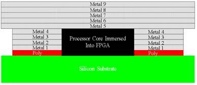
Initial Single-Event Effects Testing and Mitigation in the Xilinx Virtex II-Pro FPGA
 Initial Single-Event Effects Testing and Mitigation in the Xilinx Virtex II-Pro FPGA J. George 1, S. Rezgui 2, G. Swift 3, C. Carmichael 2 For the North American Xilinx Test Consortium 1 The Aerospace