Introduction to Field Programmable Gate Arrays
|
|
|
- Thomasina Palmer
- 5 years ago
- Views:
Transcription
1 Introduction to Field Programmable Gate Arrays Lecture 1/3 CERN Accelerator School on Digital Signal Processing Sigtuna, Sweden, 31 May 9 June 2007 Javier Serrano, CERN AB-CO-HT
2 Outline Historical introduction. Basics of digital design. FPGA structure. Traditional (HDL) design flow. Demo.
3 Outline Historical introduction. Basics of digital design. FPGA structure. Traditional (HDL) design flow. Demo.

4 Historical Introduction In the beginning, digital design was done with the 74 series of chips. Some people would design their own chips based on Gate Arrays, which were nothing else than an array of NAND gates:
5 Historical Introduction The first programmable chips were PLAs (Programmable Logic Arrays): two level structures of AND and OR gates with user programmable connections. Programmable Array Logic devices were an improvement in structure and cost over PLAs. Today such devices are generically called Programmable Logic Devices (PLDs).
 contains a much larger number of smaller individual blocks + large interconnection structure that")
6 Historical introduction A complex PLD (CPLD) is nothing else than a collection of multiple PLDs and an interconnection structure. Compared to a CPLD, a Field Programmable Gate Array (FPGA) contains a much larger number of smaller individual blocks + large interconnection structure that dominates the entire chip.
7 Outline Historical introduction. Basics of digital design. FPGA structure. Traditional (HDL) design flow. Demo.
8 Basics of digital design Unless you really know what you are doing, stick to synchronous design: sandwiching bunches of combinational logic in between flip flops. Combinational logic: state of outputs depend on current state of inputs alone (forgetting about propagation delays for the time being). E.g. AND, OR, mux, decoder, adder... D-type Flip flops propagate D to Q upon a rising edge in the clk input. Synchronous design simplifies design analysis, which is good given today s logic densities.
9 Don t do this! Toggle flip-flops get triggered by glitches produced by different path lengths of counter bits.
10 Basics of (synchronous) Digital Design Clk DataInB DataSelect DataInA D Q databc D Q dataac D[0] Q[0] dataselectc + sum 0 D Q 1 DataOut DataOut_ ns DataOut High clock rate: MHz on a Xilinx Spartan IIE. DataSelect D[0] Q[0] dataselectc D[0] Q[0] dataselectcd1 Clk DataInB D Q databc D Q dataacd1 0 D Q DataOut 1 DataOut DataOut_3 DataInA D Q dataac + D Q sum_ ns sum Higher clock rate: MHz on the same chip. Illustrating the latency/throughput tradeoff
11 Outline Historical introduction. Basics of digital design. FPGA structure. Traditional (HDL) design flow. Demo.
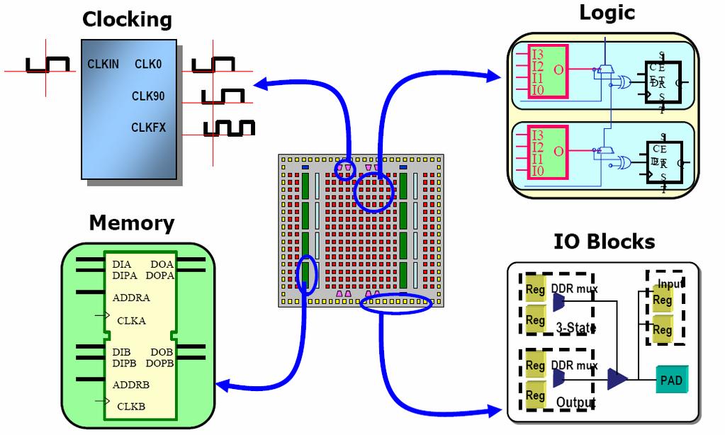
12 Basic FPGA architecture


13 The logic block: a summary view Example: using a LUT as a full adder.
 Overview")

14 A practical example: Xilinx Virtex II Pro family (used in the lab) Overview Configurable Logic Block (CLB) Embedded PowerPC Digitally Controlled Impedance (DCI)

15 A practical example: Xilinx Virtex II Pro family Slice Detail of half-slice
16 A practical example: Xilinx Virtex II Pro family Routing resources
17 FPGA state of the art In addition to logic gates and routing, in a modern FPGA you can find: Embedded processors (soft or hard). Multi-Gb/s transceivers with equalization and hard IP for serial standards as PCI Express and Gbit Ethernet. Lots of embedded MAC units, with enough bits to implement single precision floating point arithmetic efficiently. Lots of dual-port RAM. Sophisticated clock management through DLLs and PLLs. System monitoring infrastructure including ADCs. On-substrate decoupling capacitors to ease PCB design. Digitally Controlled Impedance to eliminate on-board termination resistors.
18 Embedded processors


19 Why use embedded processors? Customization: take only the peripherals you need and replicate them as many times as needed. Create your own custom peripherals. Strike optimum balance in system partitioning.

20 Serial signaling Avoids clock/data skew by using embedded clock. Reduces EMI and power consumption. Simplifies PCB routing.
21 Clock management
22 Outline Historical introduction. Basics of digital design. FPGA structure. Traditional (HDL) design flow. Demo.
23 Traditional design flow 1/3 HDL Behavioral Simulation Implement your design using VHDL or Verilog Synthesis Functional Simulation Implementation Timing Simulation Download In-Circuit Verification

24 Traditional design flow 2/3 HDL Behavioral Simulation Synthesis Functional Simulation Synthesize the design to create an FPGA netlist Implementation Timing Simulation Download In-Circuit Verification
25 Traditional design flow 3/3 HDL Behavioral Simulation Synthesis Implementation Download Functional Simulation Timing Simulation In-Circuit Verification Translate, place and route, and generate a bitstream to download in the FPGA
Field Programmable Gate Array
 Field Programmable Gate Array System Arch 27 (Fire Tom Wada) What is FPGA? System Arch 27 (Fire Tom Wada) 2 FPGA Programmable (= reconfigurable) Digital System Component Basic components Combinational
FPGA: What? Why? Marco D. Santambrogio
 FPGA: What? Why? Marco D. Santambrogio marco.santambrogio@polimi.it 2 Reconfigurable Hardware Reconfigurable computing is intended to fill the gap between hardware and software, achieving potentially much
FPGA for Complex System Implementation. National Chiao Tung University Chun-Jen Tsai 04/14/2011
 FPGA for Complex System Implementation National Chiao Tung University Chun-Jen Tsai 04/14/2011 About FPGA FPGA was invented by Ross Freeman in 1989 SRAM-based FPGA properties Standard parts Allowing multi-level
Field Programmable Gate Array (FPGA) Devices
 Devices") Field Programmable Gate Array (FPGA) Devices 1 Contents Altera FPGAs and CPLDs CPLDs FPGAs with embedded processors ACEX FPGAs Cyclone I,II FPGAs APEX FPGAs Stratix FPGAs Stratix II,III FPGAs Xilinx FPGAs
Field Programmable Gate Array (FPGA) Devices 1 Contents Altera FPGAs and CPLDs CPLDs FPGAs with embedded processors ACEX FPGAs Cyclone I,II FPGAs APEX FPGAs Stratix FPGAs Stratix II,III FPGAs Xilinx FPGAs
Topics. Midterm Finish Chapter 7
 Lecture 9 Topics Midterm Finish Chapter 7 ROM (review) Memory device in which permanent binary information is stored. Example: 32 x 8 ROM Five input lines (2 5 = 32) 32 outputs, each representing a memory
Field Programmable Gate Array (FPGA)
") Field Programmable Gate Array (FPGA) Lecturer: Krébesz, Tamas 1 FPGA in general Reprogrammable Si chip Invented in 1985 by Ross Freeman (Xilinx inc.) Combines the advantages of ASIC and uc-based systems
Field Programmable Gate Array (FPGA) Lecturer: Krébesz, Tamas 1 FPGA in general Reprogrammable Si chip Invented in 1985 by Ross Freeman (Xilinx inc.) Combines the advantages of ASIC and uc-based systems
Introduction to Field Programmable Gate Arrays
 Introduction to Field Programmable Gate Arrays Lecture 2/3 CERN Accelerator School on Digital Signal Processing Sigtuna, Sweden, 31 May 9 June 2007 Javier Serrano, CERN AB-CO-HT Outline Digital Signal
PINE TRAINING ACADEMY
 PINE TRAINING ACADEMY Course Module A d d r e s s D - 5 5 7, G o v i n d p u r a m, G h a z i a b a d, U. P., 2 0 1 0 1 3, I n d i a Digital Logic System Design using Gates/Verilog or VHDL and Implementation
INTRODUCTION TO FPGA ARCHITECTURE
 3/3/25 INTRODUCTION TO FPGA ARCHITECTURE DIGITAL LOGIC DESIGN (BASIC TECHNIQUES) a b a y 2input Black Box y b Functional Schematic a b y a b y a b y 2 Truth Table (AND) Truth Table (OR) Truth Table (XOR)
An Introduction to Programmable Logic
 Outline An Introduction to Programmable Logic 3 November 24 Transistors Logic Gates CPLD Architectures FPGA Architectures Device Considerations Soft Core Processors Design Example Quiz Semiconductors Semiconductor
Programmable Logic Devices
 Programmable Logic Devices INTRODUCTION A programmable logic device or PLD is an electronic component used to build reconfigurable digital circuits. Unlike a logic gate, which has a fixed function, a PLD
Basic FPGA Architectures. Actel FPGAs. PLD Technologies: Antifuse. 3 Digital Systems Implementation Programmable Logic Devices
 3 Digital Systems Implementation Programmable Logic Devices Basic FPGA Architectures Why Programmable Logic Devices (PLDs)? Low cost, low risk way of implementing digital circuits as application specific
EECS150 - Digital Design Lecture 6 - Field Programmable Gate Arrays (FPGAs)
") EECS150 - Digital Design Lecture 6 - Field Programmable Gate Arrays (FPGAs) September 12, 2002 John Wawrzynek Fall 2002 EECS150 - Lec06-FPGA Page 1 Outline What are FPGAs? Why use FPGAs (a short history
EECS150 - Digital Design Lecture 6 - Field Programmable Gate Arrays (FPGAs) September 12, 2002 John Wawrzynek Fall 2002 EECS150 - Lec06-FPGA Page 1 Outline What are FPGAs? Why use FPGAs (a short history
Outline. EECS150 - Digital Design Lecture 6 - Field Programmable Gate Arrays (FPGAs) FPGA Overview. Why FPGAs?
 FPGA Overview. Why FPGAs?") EECS150 - Digital Design Lecture 6 - Field Programmable Gate Arrays (FPGAs) September 12, 2002 John Wawrzynek Outline What are FPGAs? Why use FPGAs (a short history lesson). FPGA variations Internal logic
EECS150 - Digital Design Lecture 6 - Field Programmable Gate Arrays (FPGAs) September 12, 2002 John Wawrzynek Outline What are FPGAs? Why use FPGAs (a short history lesson). FPGA variations Internal logic
PLAs & PALs. Programmable Logic Devices (PLDs) PLAs and PALs
 PLAs and PALs") PLAs & PALs Programmable Logic Devices (PLDs) PLAs and PALs PLAs&PALs By the late 1970s, standard logic devices were all the rage, and printed circuit boards were loaded with them. To offer the ultimate
PLAs & PALs Programmable Logic Devices (PLDs) PLAs and PALs PLAs&PALs By the late 1970s, standard logic devices were all the rage, and printed circuit boards were loaded with them. To offer the ultimate
Basic FPGA Architecture Xilinx, Inc. All Rights Reserved
 Basic FPGA Architecture 2005 Xilinx, Inc. All Rights Reserved Objectives After completing this module, you will be able to: Identify the basic architectural resources of the Virtex -II FPGA List the differences
Digital Integrated Circuits
 Digital Integrated Circuits Lecture 9 Jaeyong Chung Robust Systems Laboratory Incheon National University DIGITAL DESIGN FLOW Chung EPC6055 2 FPGA vs. ASIC FPGA (A programmable Logic Device) Faster time-to-market
Topics. Midterm Finish Chapter 7
 Lecture 9 Topics Midterm Finish Chapter 7 Xilinx FPGAs Chapter 7 Spartan 3E Architecture Source: Spartan-3E FPGA Family Datasheet CLB Configurable Logic Blocks Each CLB contains four slices Each slice
ECE 545 Lecture 12. FPGA Resources. George Mason University
 ECE 545 Lecture 2 FPGA Resources George Mason University Recommended reading 7 Series FPGAs Configurable Logic Block: User Guide Overview Functional Details 2 What is an FPGA? Configurable Logic Blocks
Field Program mable Gate Arrays
 Field Program mable Gate Arrays M andakini Patil E H E P g r o u p D H E P T I F R SERC school NISER, Bhubaneshwar Nov 7-27 2017 Outline Digital electronics Short history of programmable logic devices
FPGA. Logic Block. Plessey FPGA: basic building block here is 2-input NAND gate which is connected to each other to implement desired function.
 FPGA Logic block of an FPGA can be configured in such a way that it can provide functionality as simple as that of transistor or as complex as that of a microprocessor. It can used to implement different
Evolution of Implementation Technologies. ECE 4211/5211 Rapid Prototyping with FPGAs. Gate Array Technology (IBM s) Programmable Logic
 Programmable Logic") ECE 42/52 Rapid Prototyping with FPGAs Dr. Charlie Wang Department of Electrical and Computer Engineering University of Colorado at Colorado Springs Evolution of Implementation Technologies Discrete devices:
ECE 42/52 Rapid Prototyping with FPGAs Dr. Charlie Wang Department of Electrical and Computer Engineering University of Colorado at Colorado Springs Evolution of Implementation Technologies Discrete devices:
FPGA Design Challenge :Techkriti 14 Digital Design using Verilog Part 1
 FPGA Design Challenge :Techkriti 14 Digital Design using Verilog Part 1 Anurag Dwivedi Digital Design : Bottom Up Approach Basic Block - Gates Digital Design : Bottom Up Approach Gates -> Flip Flops Digital
Today. Comments about assignment Max 1/T (skew = 0) Max clock skew? Comments about assignment 3 ASICs and Programmable logic Others courses
 Max clock skew? Comments about assignment 3 ASICs and Programmable logic Others courses") Today Comments about assignment 3-43 Comments about assignment 3 ASICs and Programmable logic Others courses octor Per should show up in the end of the lecture Mealy machines can not be coded in a single
Today Comments about assignment 3-43 Comments about assignment 3 ASICs and Programmable logic Others courses octor Per should show up in the end of the lecture Mealy machines can not be coded in a single
FPGAs in a Nutshell - Introduction to Embedded Systems-
 FPGAs in a Nutshell - Introduction to Embedded Systems- Dipl.- Ing. Falk Salewski Lehrstuhl Informatik RWTH Aachen salewski@informatik.rwth-aachen.de Winter term 6/7 Contents History FPGA architecture
VHDL for Synthesis. Course Description. Course Duration. Goals
 VHDL for Synthesis Course Description This course provides all necessary theoretical and practical know how to write an efficient synthesizable HDL code through VHDL standard language. The course goes
FPGA architecture and design technology
 CE 435 Embedded Systems Spring 2017 FPGA architecture and design technology Nikos Bellas Computer and Communications Engineering Department University of Thessaly 1 FPGA fabric A generic island-style FPGA
Introduction to FPGAs. H. Krüger Bonn University
 Introduction to FPGAs H. Krüger Bonn University Outline 1. History 2. FPGA Architecture 3. Current Trends 4. Design Methodology (short see other lectures) Disclaimer: Most of the resources used for this
Digital Design with FPGAs. By Neeraj Kulkarni
 Digital Design with FPGAs By Neeraj Kulkarni Some Basic Electronics Basic Elements: Gates: And, Or, Nor, Nand, Xor.. Memory elements: Flip Flops, Registers.. Techniques to design a circuit using basic
EE178 Lecture Module 2. Eric Crabill SJSU / Xilinx Fall 2007
 EE178 Lecture Module 2 Eric Crabill SJSU / Xilinx Fall 2007 Lecture #4 Agenda Survey of implementation technologies. Implementation Technologies Small scale and medium scale integration. Up to about 200
ISE Design Suite Software Manuals and Help
 ISE Design Suite Software Manuals and Help These documents support the Xilinx ISE Design Suite. Click a document title on the left to view a document, or click a design step in the following figure to
Programmable Logic. Any other approaches?
 Programmable Logic So far, have only talked about PALs (see 22V10 figure next page). What is the next step in the evolution of PLDs? More gates! How do we get more gates? We could put several PALs on one
Overview. CSE372 Digital Systems Organization and Design Lab. Hardware CAD. Two Types of Chips
 Overview CSE372 Digital Systems Organization and Design Lab Prof. Milo Martin Unit 5: Hardware Synthesis CAD (Computer Aided Design) Use computers to design computers Virtuous cycle Architectural-level,
Lecture 7. Standard ICs FPGA (Field Programmable Gate Array) VHDL (Very-high-speed integrated circuits. Hardware Description Language)
 VHDL (Very-high-speed integrated circuits. Hardware Description Language)") Standard ICs FPGA (Field Programmable Gate Array) VHDL (Very-high-speed integrated circuits Hardware Description Language) 1 Standard ICs PLD: Programmable Logic Device CPLD: Complex PLD FPGA: Field Programmable
Standard ICs FPGA (Field Programmable Gate Array) VHDL (Very-high-speed integrated circuits Hardware Description Language) 1 Standard ICs PLD: Programmable Logic Device CPLD: Complex PLD FPGA: Field Programmable
Lab 3 Sequential Logic for Synthesis. FPGA Design Flow.
 Lab 3 Sequential Logic for Synthesis. FPGA Design Flow. Task 1 Part 1 Develop a VHDL description of a Debouncer specified below. The following diagram shows the interface of the Debouncer. The following
Lecture 3: Modeling in VHDL. EE 3610 Digital Systems
 EE 3610: Digital Systems 1 Lecture 3: Modeling in VHDL VHDL: Overview 2 VHDL VHSIC Hardware Description Language VHSIC=Very High Speed Integrated Circuit Programming language for modelling of hardware
Summary. Introduction. Application Note: Virtex, Virtex-E, Spartan-IIE, Spartan-3, Virtex-II, Virtex-II Pro. XAPP152 (v2.1) September 17, 2003
 September 17, 2003") Application Note: Virtex, Virtex-E, Spartan-IIE, Spartan-3, Virtex-II, Virtex-II Pro Xilinx Tools: The Estimator XAPP152 (v2.1) September 17, 2003 Summary This application note is offered as complementary
Application Note: Virtex, Virtex-E, Spartan-IIE, Spartan-3, Virtex-II, Virtex-II Pro Xilinx Tools: The Estimator XAPP152 (v2.1) September 17, 2003 Summary This application note is offered as complementary
EECS150 - Digital Design Lecture 16 - Memory
 EECS150 - Digital Design Lecture 16 - Memory October 17, 2002 John Wawrzynek Fall 2002 EECS150 - Lec16-mem1 Page 1 Memory Basics Uses: data & program storage general purpose registers buffering table lookups
ECE 331 Digital System Design
 ECE 331 Digital System Design Tristate Buffers, Read-Only Memories and Programmable Logic Devices (Lecture #17) The slides included herein were taken from the materials accompanying Fundamentals of Logic
Verilog for High Performance
 Verilog for High Performance Course Description This course provides all necessary theoretical and practical know-how to write synthesizable HDL code through Verilog standard language. The course goes
Hardware Synthesis. References
 Hardware Synthesis MidiaReshadi CE Department Science and research branch of Islamic Azad University Email: ce.srbiau@gmail.com 1 References 2 1 Chapter 1 Digital Design Using VHDL and PLDs 3 Some Definitions
Chapter 10: Design Options of Digital Systems
 Chapter 10: Design Options of Digital Systems Prof. Ming-Bo Lin Department of Electronic Engineering National Taiwan University of Science and Technology Digital System Designs and Practices Using Verilog
EE219A Spring 2008 Special Topics in Circuits and Signal Processing. Lecture 9. FPGA Architecture. Ranier Yap, Mohamed Ali.
 EE219A Spring 2008 Special Topics in Circuits and Signal Processing Lecture 9 FPGA Architecture Ranier Yap, Mohamed Ali Annoucements Homework 2 posted Due Wed, May 7 Now is the time to turn-in your Hw
FPGA Based Digital Design Using Verilog HDL
 FPGA Based Digital Design Using Course Designed by: IRFAN FAISAL MIR ( Verilog / FPGA Designer ) irfanfaisalmir@yahoo.com * Organized by Electronics Division Integrated Circuits Uses for digital IC technology
CS310 Embedded Computer Systems. Maeng
 1 INTRODUCTION (PART II) Maeng Three key embedded system technologies 2 Technology A manner of accomplishing a task, especially using technical processes, methods, or knowledge Three key technologies for
Signal Processing Algorithms into Fixed Point FPGA Hardware Dennis Silage ECE Temple University
 Signal Processing Algorithms into Fixed Point FPGA Hardware Dennis Silage silage@temple.edu ECE Temple University www.temple.edu/scdl Signal Processing Algorithms into Fixed Point FPGA Hardware Motivation
CPE/EE 422/522. Introduction to Xilinx Virtex Field-Programmable Gate Arrays Devices. Dr. Rhonda Kay Gaede UAH. Outline
 CPE/EE 422/522 Introduction to Xilinx Virtex Field-Programmable Gate Arrays Devices Dr. Rhonda Kay Gaede UAH Outline Introduction Field-Programmable Gate Arrays Virtex Virtex-E, Virtex-II, and Virtex-II
Hardware Design with VHDL PLDs IV ECE 443
 Embedded Processor Cores (Hard and Soft) Electronic design can be realized in hardware (logic gates/registers) or software (instructions executed on a microprocessor). The trade-off is determined by how
Experiment 3. Digital Circuit Prototyping Using FPGAs
 Experiment 3. Digital Circuit Prototyping Using FPGAs Masud ul Hasan Muhammad Elrabaa Ahmad Khayyat Version 151, 11 September 2015 Table of Contents 1. Objectives 2. Materials Required 3. Background 3.1.
Outline. Field Programmable Gate Arrays. Programming Technologies Architectures. Programming Interfaces. Historical perspective
 Outline Field Programmable Gate Arrays Historical perspective Programming Technologies Architectures PALs, PLDs,, and CPLDs FPGAs Programmable logic Interconnect network I/O buffers Specialized cores Programming
EECS 150 Homework 7 Solutions Fall (a) 4.3 The functions for the 7 segment display decoder given in Section 4.3 are:
 4.3 The functions for the 7 segment display decoder given in Section 4.3 are:") Problem 1: CLD2 Problems. (a) 4.3 The functions for the 7 segment display decoder given in Section 4.3 are: C 0 = A + BD + C + BD C 1 = A + CD + CD + B C 2 = A + B + C + D C 3 = BD + CD + BCD + BC C 4
Problem 1: CLD2 Problems. (a) 4.3 The functions for the 7 segment display decoder given in Section 4.3 are: C 0 = A + BD + C + BD C 1 = A + CD + CD + B C 2 = A + B + C + D C 3 = BD + CD + BCD + BC C 4
FPGA for Software Engineers
 FPGA for Software Engineers Course Description This course closes the gap between hardware and software engineers by providing the software engineer all the necessary FPGA concepts and terms. The course
EITF35: Introduction to Structured VLSI Design
 EITF35: Introduction to Structured VLSI Design Introduction to FPGA design Rakesh Gangarajaiah Rakesh.gangarajaiah@eit.lth.se Slides from Chenxin Zhang and Steffan Malkowsky WWW.FPGA What is FPGA? Field
EECS150 - Digital Design Lecture 16 Memory 1
 EECS150 - Digital Design Lecture 16 Memory 1 March 13, 2003 John Wawrzynek Spring 2003 EECS150 - Lec16-mem1 Page 1 Memory Basics Uses: Whenever a large collection of state elements is required. data &
Programmable Logic Devices FPGA Architectures II CMPE 415. Overview This set of notes introduces many of the features available in the FPGAs of today.
 Overview This set of notes introduces many of the features available in the FPGAs of today. The majority use SRAM based configuration cells, which allows fast reconfiguation. Allows new design ideas to
High Capacity and High Performance 20nm FPGAs. Steve Young, Dinesh Gaitonde August Copyright 2014 Xilinx
 High Capacity and High Performance 20nm FPGAs Steve Young, Dinesh Gaitonde August 2014 Not a Complete Product Overview Page 2 Outline Page 3 Petabytes per month Increasing Bandwidth Global IP Traffic Growth
Graduate Institute of Electronics Engineering, NTU FPGA Design with Xilinx ISE
 FPGA Design with Xilinx ISE Presenter: Shu-yen Lin Advisor: Prof. An-Yeu Wu 2005/6/6 ACCESS IC LAB Outline Concepts of Xilinx FPGA Xilinx FPGA Architecture Introduction to ISE Code Generator Constraints
FPGA Design Flow 1. All About FPGA
 FPGA Design Flow 1 In this part of tutorial we are going to have a short intro on FPGA design flow. A simplified version of FPGA design flow is given in the flowing diagram. FPGA Design Flow 2 FPGA_Design_FLOW
Chapter 9: Integration of Full ASIP and its FPGA Implementation
 Chapter 9: Integration of Full ASIP and its FPGA Implementation 9.1 Introduction A top-level module has been created for the ASIP in VHDL in which all the blocks have been instantiated at the Register
EE260: Digital Design, Spring 2018
 Topics Verilog Module 1 Introduction Yao Zheng (Based on the slides of Prof. Jim Duckworth) Background to Verilog Introduction to language Programmable Logic Devices CPLDs and FPGAs FPGA architecture Nexys
Tutorial on VHDL and Verilog Applications
 Second LACCEI International Latin American and Caribbean Conference for Engineering and Technology (LACCEI 2004) Challenges and Opportunities for Engineering Education, Research and Development 2-4 June
TLL5000 Electronic System Design Base Module. Getting Started Guide, Ver 3.4
 TLL5000 Electronic System Design Base Module Getting Started Guide, Ver 3.4 COPYRIGHT NOTICE The Learning Labs, Inc. ( TLL ) All rights reserved, 2008 Reproduction in any form without permission is prohibited.
Xilinx ASMBL Architecture
 FPGA Structure Xilinx ASMBL Architecture Design Flow Synthesis: HDL to FPGA primitives Translate: FPGA Primitives to FPGA Slice components Map: Packing of Slice components into Slices, placement of Slices
Verilog Sequential Logic. Verilog for Synthesis Rev C (module 3 and 4)
") Verilog Sequential Logic Verilog for Synthesis Rev C (module 3 and 4) Jim Duckworth, WPI 1 Sequential Logic Module 3 Latches and Flip-Flops Implemented by using signals in always statements with edge-triggered
Verilog Sequential Logic Verilog for Synthesis Rev C (module 3 and 4) Jim Duckworth, WPI 1 Sequential Logic Module 3 Latches and Flip-Flops Implemented by using signals in always statements with edge-triggered
EECS150 - Digital Design Lecture 10 Logic Synthesis
 EECS150 - Digital Design Lecture 10 Logic Synthesis September 26, 2002 John Wawrzynek Fall 2002 EECS150 Lec10-synthesis Page 1 Logic Synthesis Verilog and VHDL stated out as simulation languages, but quickly
ECE 645: Lecture 1. Basic Adders and Counters. Implementation of Adders in FPGAs
 ECE 645: Lecture Basic Adders and Counters Implementation of Adders in FPGAs Required Reading Behrooz Parhami, Computer Arithmetic: Algorithms and Hardware Design Chapter 5, Basic Addition and Counting,
EECS150 - Digital Design Lecture 5 - Verilog Logic Synthesis
 EECS150 - Digital Design Lecture 5 - Verilog Logic Synthesis Jan 31, 2012 John Wawrzynek Spring 2012 EECS150 - Lec05-verilog_synth Page 1 Outline Quick review of essentials of state elements Finite State
CSE140L: Components and Design Techniques for Digital Systems Lab
 CSE140L: Components and Design Techniques for Digital Systems Lab Tajana Simunic Rosing Source: Vahid, Katz, Culler 1 Announcements & Outline Lab 4 due; demo signup times listed on the cse140l site Check
Memory and Programmable Logic
 Memory and Programmable Logic Memory units allow us to store and/or retrieve information Essentially look-up tables Good for storing data, not for function implementation Programmable logic device (PLD),
Spiral 2-8. Cell Layout
 2-8.1 Spiral 2-8 Cell Layout 2-8.2 Learning Outcomes I understand how a digital circuit is composed of layers of materials forming transistors and wires I understand how each layer is expressed as geometric
Using XILINX WebPACK Software to Create CPLD Designs
 Introduction to WebPACK Using XILINX WebPACK Software to Create CPLD Designs RELEASE DATE: 10/24/1999 All XS-prefix product designations are trademarks of XESS Corp. All XC-prefix product designations
Lecture #1: Introduction
 Lecture #1: Introduction Kunle Olukotun Stanford EE183 January 8, 20023 What is EE183? EE183 is continuation of EE121 Digital Logic Design is a a minute to learn, a lifetime to master Programmable logic
INTRODUCTION TO FIELD PROGRAMMABLE GATE ARRAYS (FPGAS)
") INTRODUCTION TO FIELD PROGRAMMABLE GATE ARRAYS (FPGAS) Bill Jason P. Tomas Dept. of Electrical and Computer Engineering University of Nevada Las Vegas FIELD PROGRAMMABLE ARRAYS Dominant digital design
INTRODUCTION TO FIELD PROGRAMMABLE GATE ARRAYS (FPGAS) Bill Jason P. Tomas Dept. of Electrical and Computer Engineering University of Nevada Las Vegas FIELD PROGRAMMABLE ARRAYS Dominant digital design
Introduction to Modern FPGAs
 Introduction to Modern FPGAs Arturo Díaz Pérez Centro de Investigación y de Estudios Avanzados del IPN Departamento de Ingeniería Eléctrica Sección de Computación adiaz@cs.cinvestav.mx Outline Technology
Product Obsolete/Under Obsolescence
 APPLICATION NOTE Adapting ASIC Designs for Use with Spartan FPGAs XAPP119 July 20, 1998 (Version 1.0) Application Note by Kim Goldblatt Summary Spartan FPGAs are an exciting, new alternative for implementing
(ii) Simplify and implement the following SOP function using NOR gates:
 Simplify and implement the following SOP function using NOR gates:") DHANALAKSHMI COLLEGE OF ENGINEERING DEPARTMENT OF ELECTRONICS AND COMMUNICATION ENGINEERING EE6301 DIGITAL LOGIC CIRCUITS UNIT I NUMBER SYSTEMS AND DIGITAL LOGIC FAMILIES PART A 1. How can an OR gate be
DHANALAKSHMI COLLEGE OF ENGINEERING DEPARTMENT OF ELECTRONICS AND COMMUNICATION ENGINEERING EE6301 DIGITAL LOGIC CIRCUITS UNIT I NUMBER SYSTEMS AND DIGITAL LOGIC FAMILIES PART A 1. How can an OR gate be
System-on Solution from Altera and Xilinx
 System-on on-a-programmable-chip Solution from Altera and Xilinx Xun Yang VLSI CAD Lab, Computer Science Department, UCLA FPGAs with Embedded Microprocessors Combination of embedded processors and programmable
ispxpld TM 5000MX Family White Paper
 ispxpld TM 5000MX Family White Paper October 2002 Overview The two largest segments of the high density programmable logic market have traditionally been nonvolatile, Complex Programmable Logic Devices
VLSI Test Technology and Reliability (ET4076)
") VLSI Test Technology and Reliability (ET4076) Lecture 4(part 2) Testability Measurements (Chapter 6) Said Hamdioui Computer Engineering Lab Delft University of Technology 2009-2010 1 Previous lecture What
VLSI Test Technology and Reliability (ET4076) Lecture 4(part 2) Testability Measurements (Chapter 6) Said Hamdioui Computer Engineering Lab Delft University of Technology 2009-2010 1 Previous lecture What
MASSACHUSETTS INSTITUTE OF TECHNOLOGY Department of Electrical Engineering and Computer Sciences
 MASSACHUSETTS INSTITUTE OF TECHNOLOGY Department of Electrical Engineering and Computer Sciences Introductory Digital Systems Lab (6.111) uiz - Spring 2004 Prof. Anantha Chandrakasan Student Name: Problem
: : (91-44) (Office) (91-44) (Residence)
 (Office) (91-44) (Residence)") Course: VLSI Circuits (Video Course) Faculty Coordinator(s) : Prof. S. Srinivasan Department of Electrical Engineering Indian Institute of Technology Madras Chennai 600036 Email Telephone : srinis@iitm.ac.in,
Course: VLSI Circuits (Video Course) Faculty Coordinator(s) : Prof. S. Srinivasan Department of Electrical Engineering Indian Institute of Technology Madras Chennai 600036 Email Telephone : srinis@iitm.ac.in,
VHX - Xilinx - FPGA Programming in VHDL
 Training Xilinx - FPGA Programming in VHDL: This course explains how to design with VHDL on Xilinx FPGAs using ISE Design Suite - Programming: Logique Programmable VHX - Xilinx - FPGA Programming in VHDL
Synthesis of VHDL Code for FPGA Design Flow Using Xilinx PlanAhead Tool
 Synthesis of VHDL Code for FPGA Design Flow Using Xilinx PlanAhead Tool Md. Abdul Latif Sarker, Moon Ho Lee Division of Electronics & Information Engineering Chonbuk National University 664-14 1GA Dekjin-Dong
Design Progression With VHDL Helps Accelerate The Digital System Designs
 Fourth LACCEI International Latin American and Caribbean Conference for Engineering and Technology (LACCET 2006) Breaking Frontiers and Barriers in Engineering: Education, Research and Practice 21-23 June
FPGA Implementations
 FPGA Implementations Smith Text: Chapters 4-8 Online version at: http://www10.edacafe.com/book/asic/asics.php Topic outline Chapter 4 Programmable ASIC technologies Chapter 5 Programmable logic cells Chapter
CSE140L: Components and Design
 CSE140L: Components and Design Techniques for Digital Systems Lab Tajana Simunic Rosing Source: Vahid, Katz, Culler 1 Grade distribution: 70% Labs 35% Lab 4 30% Lab 3 20% Lab 2 15% Lab 1 30% Final exam
Don t expect to be able to write and debug your code during the lab session.
 EECS150 Spring 2002 Lab 4 Verilog Simulation Mapping UNIVERSITY OF CALIFORNIA AT BERKELEY COLLEGE OF ENGINEERING DEPARTMENT OF ELECTRICAL ENGINEERING AND COMPUTER SCIENCE Lab 4 Verilog Simulation Mapping
Code No: R Set No. 1
 Code No: R059210504 Set No. 1 II B.Tech I Semester Regular Examinations, November 2006 DIGITAL LOGIC DESIGN ( Common to Computer Science & Engineering, Information Technology and Computer Science & Systems
Note: Closed book no notes or other material allowed, no calculators or other electronic devices.
 ECE 574: Modeling and Synthesis of Digital Systems using Verilog and VHDL Fall 2017 Exam Review Note: Closed book no notes or other material allowed, no calculators or other electronic devices. One page
CONTENTS CHAPTER 1: NUMBER SYSTEM. Foreword...(vii) Preface... (ix) Acknowledgement... (xi) About the Author...(xxiii)
 Preface... (ix) Acknowledgement... (xi) About the Author...(xxiii)") CONTENTS Foreword...(vii) Preface... (ix) Acknowledgement... (xi) About the Author...(xxiii) CHAPTER 1: NUMBER SYSTEM 1.1 Digital Electronics... 1 1.1.1 Introduction... 1 1.1.2 Advantages of Digital Systems...
CONTENTS Foreword...(vii) Preface... (ix) Acknowledgement... (xi) About the Author...(xxiii) CHAPTER 1: NUMBER SYSTEM 1.1 Digital Electronics... 1 1.1.1 Introduction... 1 1.1.2 Advantages of Digital Systems...
Graduate course on FPGA design
 History of and programmable logic February 15, 2010 History of and programmable logic History of and programmable logic History of and programmable logic Course planning Lectures Laboration 4 HP for actively
Virtex-II Architecture. Virtex II technical, Design Solutions. Active Interconnect Technology (continued)
") Virtex-II Architecture SONET / SDH Virtex II technical, Design Solutions PCI-X PCI DCM Distri RAM 18Kb BRAM Multiplier LVDS FIFO Shift Registers BLVDS SDRAM QDR SRAM Backplane Rev 4 March 4th. 2002 J-L
Virtex-II Architecture SONET / SDH Virtex II technical, Design Solutions PCI-X PCI DCM Distri RAM 18Kb BRAM Multiplier LVDS FIFO Shift Registers BLVDS SDRAM QDR SRAM Backplane Rev 4 March 4th. 2002 J-L
Lecture 2 Hardware Description Language (HDL): VHSIC HDL (VHDL)
: VHSIC HDL (VHDL)") Lecture 2 Hardware Description Language (HDL): VHSIC HDL (VHDL) Pinit Kumhom VLSI Laboratory Dept. of Electronic and Telecommunication Engineering (KMUTT) Faculty of Engineering King Mongkut s University
Lecture 2 Hardware Description Language (HDL): VHSIC HDL (VHDL) Pinit Kumhom VLSI Laboratory Dept. of Electronic and Telecommunication Engineering (KMUTT) Faculty of Engineering King Mongkut s University
Scalable and Dynamically Updatable Lookup Engine for Decision-trees on FPGA
 Scalable and Dynamically Updatable Lookup Engine for Decision-trees on FPGA Yun R. Qu, Viktor K. Prasanna Ming Hsieh Dept. of Electrical Engineering University of Southern California Los Angeles, CA 90089
KINGS COLLEGE OF ENGINEERING DEPARTMENT OF ELECTRICAL AND ELECTRONICS ENGINEERING QUESTION BANK NAME OF THE SUBJECT: EE 2255 DIGITAL LOGIC CIRCUITS
 KINGS COLLEGE OF ENGINEERING DEPARTMENT OF ELECTRICAL AND ELECTRONICS ENGINEERING QUESTION BANK NAME OF THE SUBJECT: EE 2255 DIGITAL LOGIC CIRCUITS YEAR / SEM: II / IV UNIT I BOOLEAN ALGEBRA AND COMBINATIONAL
structure syntax different levels of abstraction
 This and the next lectures are about Verilog HDL, which, together with another language VHDL, are the most popular hardware languages used in industry. Verilog is only a tool; this course is about digital
Here is a list of lecture objectives. They are provided for you to reflect on what you are supposed to learn, rather than an introduction to this
 This and the next lectures are about Verilog HDL, which, together with another language VHDL, are the most popular hardware languages used in industry. Verilog is only a tool; this course is about digital
AL8253 Core Application Note
 AL8253 Core Application Note 6-15-2012 Table of Contents General Information... 3 Features... 3 Block Diagram... 3 Contents... 4 Behavioral... 4 Synthesizable... 4 Test Vectors... 4 Interface... 5 Implementation
EECS150, Fall 2004, Midterm 1, Prof. Culler. Problem 1 (15 points) 1.a. Circle the gate-level circuits that DO NOT implement a Boolean AND function.
 1.a. Circle the gate-level circuits that DO NOT implement a Boolean AND function.") Problem 1 (15 points) 1.a. Circle the gate-level circuits that DO NOT implement a Boolean AND function. 1.b. Show that a 2-to-1 MUX is universal (i.e. that any Boolean expression can be implemented with
Problem 1 (15 points) 1.a. Circle the gate-level circuits that DO NOT implement a Boolean AND function. 1.b. Show that a 2-to-1 MUX is universal (i.e. that any Boolean expression can be implemented with
V8-uRISC 8-bit RISC Microprocessor AllianceCORE Facts Core Specifics VAutomation, Inc. Supported Devices/Resources Remaining I/O CLBs
 V8-uRISC 8-bit RISC Microprocessor February 8, 1998 Product Specification VAutomation, Inc. 20 Trafalgar Square Nashua, NH 03063 Phone: +1 603-882-2282 Fax: +1 603-882-1587 E-mail: sales@vautomation.com