CS310 Embedded Computer Systems. Maeng
|
|
|
- Jerome Baker
- 5 years ago
- Views:
Transcription
1 1 INTRODUCTION (PART II) Maeng
2 Three key embedded system technologies 2 Technology A manner of accomplishing a task, especially using technical processes, methods, or knowledge Three key technologies for embedded systems Processor technology ogy IC technology Design technology From Chapter 1, Embedded system design: A unified HW/SW introduction, Frank Vahid/Tony Givargis.
3 3 Processor Technology
4 Processor technology 4 The architecture of the computation engine used to implement a system s desired functionality Processor does not have to be programmable Processor not equal to general-purpose processor Controller Datapath Controller Datapath Controller Datapath Control logic and State register Register file General IR PC ALU Control logic and State register IR PC Registers Custom ALU Control logic State register index total + Data memory Data memory Program memory Assembly code for: Data memory Program memory Assembly code for: total = 0 for i =1 to General-purpose ( software ) total = 0 for i =1 to Application-specific Single-purpose ( hardware )
5 Processor technology 5 Processors vary in their customization for the problem at hand Desired functionality total = 0 for i = 1toN loop total += M[i] end loop General-purpose processor Application-specific processor Single-purpose processor
6 General-purpose processors 6 Programmable device used in a variety of Controller applications Control Also known as microprocessor logic and State Features register Program memory General datapath with large register file and IR PC general ALU User benefits Program memory Low time-to-market t t and NRE costs Assembly High flexibility code for: Pentium the most well-known, but there are hundreds of others total = 0 for i =1 to Datapath Register file General ALU Data memory
7 Single-purpose processors 7 Digital it circuit it designed d to execute exactly one program a.k.a. coprocessor, accelerator or peripheral Features Contains only the components needed to execute a single program Controller Control logic State register Datapath index total + No program memory Benefits Data memory Fast Low power Small size
8 8 Application-specific processors Programmable processor optimized for a Controller Dt Datapathth particular class of applications having common Control Registers characteristics logic and Compromise between general-purpose and single-purpose processors Features Program memory Optimized datapath Special functional units Benefits Some flexibility, good performance, size and power State register IR PC Program memory Assembly code for: total = 0 for i =1 to Custom ALU Data memory TI s TMS320 digital signal processor
9 9 IC Technology
 implementation is mapped onto an")

 IC technologies differ")

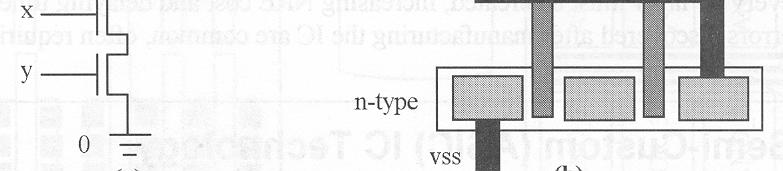
10 IC technology 10 The manner in which a digital (gate-level) implementation is mapped onto an IC IC: Integrated circuit, or chip IC technologies differ in their customization to a design IC s consist of numerous layers (perhaps 10 or more) IC technologies differ with respect to who builds each layer and when IC package IC source gate oxide channel drain Silicon substrate
11 IC technology 11 Three types of IC technologies Full-custom/VLSI Semi-custom ASIC (gate array and standard cell) PLD (Programmable Logic Device)
12 Outline 12 Anatomy of integrated circuits Full-Custom (VLSI) IC Technology Semi-Custom (ASIC) IC Technology Programmable Logic Device (PLD) IC Technology


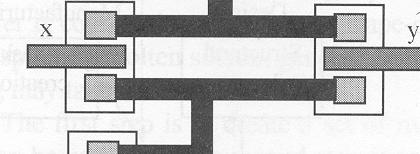
13 MOS transistor 13 Source, Drain Gate Diffusion area where electrons can flow Can be connected to metal contacts (via s) Polysilicon area where control voltage is applied Oxide Si O 2 Insulator so the gate voltage can t leak
14 NMOS Transistor fabrication process(1) 14 NMOS Transistor(NMOS FET) S i O 2 Silicon dioxide(0.6 micron) is grown all over the surface P type silicon Ultra-violet light Mask P type silicon Photo-resist material S i O 2 Photolithography S i O 2 Silicon dioxide( 산화막 )(about 0.6 micron) P type silicon
15 NMOS Transistor fabrication process(2) 15 gate oxide(about 0.05 micron) is grown Polysilicon is deposited (Low Pressure Chemical Vapor Deposition) Diffuse A S (n type) Source, drain structures are formed n+ n+
16 NMOS Transistor fabrication process(3) 16 n+ n+ SiO2 is grown deposit metal(aluminium) to make contact points n+ n+ Length unit --- λ (micron) 2λ λ
17 Four views 17 Logic Transistor Layout Physical
18 NAND 18 Metal layers for routing (~10) A stick diagram form the basis for mask sets (layout)
19 IC manufacturing steps 19 Structural t design from functional descriptions to the optimized i circuits it at gate level Layout design from the gate level descriptions to the physical layout Tape out Send design to manufacturing Photolithography Drawing patterns by using photo-resist to form barriers for deposition Tape-out
 Placement")


20 Full Custom 20 Very Large Scale Integration ti (VLSI) Placement Place and orient transistors Routing Connect transistors Sizingi Make fat, fast wires or thin, slow wires May also need to size buffer Design Rules simple i l rules for correct circuit it function Metal/metal spacing, min poly width


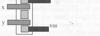
21 Full Custom 21 Best size, power, performance Hand design Horrible time-to-market/flexibility/nre cost Reserve for the most important units in a processor ALU, Instruction fetch Physical design tools Less optimal, but faster Vdd
22 Semi-custom 22 Lower layers are fully or partially built Designers are left with routing of wires and maybe placing some blocks Benefits Good performance, good size, less NRE cost than a full-custom implementation (perhaps $10k to $100k) Drawbacks Still require weeks to months to develop


23 Semi-Custom 23 Gate Array Array of prefabricated gates place and route Higher density, faster time-to-market Does not integrate as well with full-custom Standard Cell A library of pre-designed cell Place and route Lower density, higher complexity Integrate great with full-custom
24 ASea-of-gates gate array 24 f 1 x 1 x 2 x 3 The logic function f 1 = x 2 x 3 +x 1 x 3 in the gate array
25 A section of two rows in a standard cell 25 x 1 f 2 x 2 x 3 f 1 f 1 = x 1 x 2 +x 1 x 3 +x 1 x 2 x 3 f2 = x 1x 2+x 1x 2x 3+x 1x 3
26 Semi-Custom 26 Most popular design style Jack of all trade Good Power, time-to-market, performance, NRE cost, per-unit cost, area Master of none Standard-cell integrated with full custom for critical regions of design
27 Programmable Logic Devices 27 Programmable Logic Device Programmable Logic Array, Programmable Array Logic, Field Programmable Gate Array All layers already exist Designers can purchase an IC To implement desired functionality Connections on the IC are either created or destroyed to implement Benefits Very low NRE costs Great Time to Market Drawbacks High unit cost, bad for large volume Power Except special PLA Slower 1600 usable gate, 7.5 ns $7 list price
28 Programmable Logic Array (PLA) 28 Pre-fabricated building block of many AND/OR gates personalized by making or breaking connections among the gates Programmable array block diagram for sum of products form x 1 x 2 x n Input buffers and inverters x 1 x 1 x n x n AND plane P 1 P k OR plane f 1 f m
29 Gate-level Diagram of a PLA 29 x 1 x 2 x 3 Programmable connections P 1 OR plane P2 P 3 P 4 Product terms AND plane f 1 f 2 f 1 and f 2?? Sum of Product terms
30 Programmable Array Logic (PAL) 30 x 1 x 2 x 3 Programmable P 1 Fixed Hardwired P 2 f 1 P 3 P 4 f 2 What is the difference? AND plane
31 Field-Programmable Gate Arrays (FPGAs) 31 FPGAs are programmable devices that support relatively large circuits Macrocell of PLDs : 20 gates PAL : 8 macrocell (160 gates) CPLD : 500 macrocell (10,000 gates) Altera 40nm Stratix IV in 2008 Over 2.5 billion TRs, 8.1 M ASIC gate equivalent Different from CPLDs since they do not contain AND and OR planes Provide logic blocks for implementing the logic functions Three main types of resources Logic blocks I/O blocks Interconnection wires

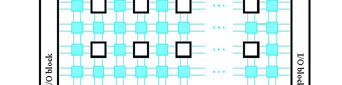
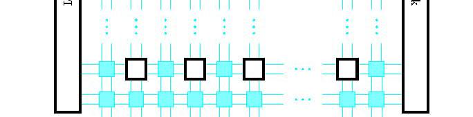

32 Structure of an FPGA 32
33 Logic Blocks 33 Each block has a small number of inputs and one output Usually use lookup tables (LUT) Contains storage cells used to implement a small logic function Each storage cell can hold a 0 or a 1 Stored value is produced as the output of the storage cell
34 Atwo-input lookup table 34 x 1 0/1 x 2 0/1 f x 1 x 2 f 1 0/ / (a) Circuit for a two-input LUT (b) f 1 = x 1 x 2 + x 1 x 2 x 1 If x 1 = f 1 0 x 2 If x 2 =1 2 (c) Storage cell contents in the LUT
35 A three-input LUT 35 x 1 x 2 0/1 0/1 0/1 0/1 0/1 0/1 0/1 0/1 f x 3
36 Inclusion of a flip-flop flop in an FPGA logic block 36 Select Flip-flop In 1 D Q Out In 2 In 3 LUT Clock
37 A section of a programmed FPGA 37 x 3 f f=x 1 x 2 +x 2 x 3 x 1 x 2 x 1 0 x f f 0 2 x 2 x f 1 f f

38 Xilinx FPGA 38
39 Configurable Logic Block (CLB) 39
40 I/O Block 40


41 41 Cyclone II FPGA
42 Altera Cyclone II Device 42 Features 90-nm low-k dielectric process High density architecture with 4,608 to 68,416 LEs Up to 1.1 Mbits of RAM Variable port configurations (x1, x2, x4, x8, x16, x32, and x36) True dual-port operations Up to 260MHz operation Embedded Multipliers Advanced I/O support Flexible clock management circuitry Hierarchical clock network for up to MHz Up to 4 PLLs Up to 16 global clock lines
43 Cyclone II FPGA Family Features 43-6 is the fastest
44 Cyclone II Architecture 44 Two-dimensional row- and column-based architecture Logic Array Logic Array Block (LAB): 16 logic elements (LEs) LE : small unit of logic providing efficient programming of user logic functions 4,608 LEs (288 LABs) to 68,416 LEs (4,276 LABs) Input/Output element (IOE) Global network and up to 4 PLLs M4K memory blocks Embedded multiplier blocks Advanced I/O pins


45 45 Cyclone II EP2C20 Block Diagram
46 Logic Elements 46 Af four-input look-up table (LUT) Can implement any function of four variables A programmable register A carry chain connection A register chain connection The ability to drive all types of interconnections Local, row, column, register chain, and direct link interconnects Support for register packing Support for register feedback
47 Cyclone II LE diagram 47
48 LE Operating Modes 48 Normal Mode
49 LE Operating Modes, cont d 49 Arithmetic Mode
50 Logic Array Blocks 50 LAB 16 LEs LAB control signals LE carry chains Register chains Local Interconnect Transfer signals between LEs in the same LAB
51 LAB Structure 51
52 LAB interconnects 52 Each LE can drive 48 LEs through fast local and direct link interconnects
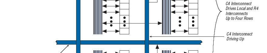
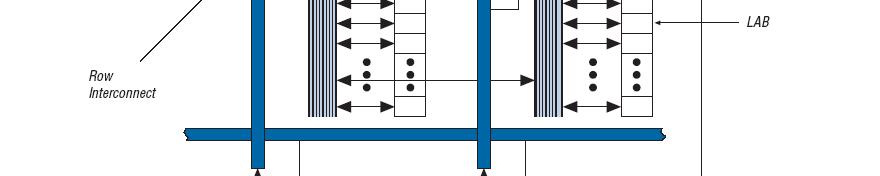
53 Multi-track track Interconnect 53 Connections between LEs, M4K memory blocks, embedded multipliers, and I/O pins Consists of row and column interconnects that span fixed distances Row direct link, R4, and R24 Column register chain, C4, and C16
54 Row interconnects 54


55 55 Column interconnects

56 Global Clock Networks & PLLs 56
57 I/O Structure and Features 57 Differential and single-ended I/O standards 3.3-V, 64- and 32-bit, 66- and 33-MHz PCI compliance JTAG boundary-scan test (BST) support
58 IOE Structure 58
59 59 Independence of processor and IC technologies Basic tradeoff General vs. custom With respect to processor technology or IC technology The two technologies are independent General, providing improved: Flexibility Maintainability NRE cost Time- to-prototype Time-to-market Cost (low volume) General- Singlepurpose ASP purpose processor processor Customized, providing improved: Power efficiency Performance Size Cost (high volume) PLD Semi-custom Full-custom
Design Metrics. A couple of especially important metrics: Time to market Total cost (NRE + unit cost) Performance (speed latency and throughput)
 Performance (speed latency and throughput)") Design Metrics A couple of especially important metrics: Time to market Total cost (NRE + unit cost) Performance (speed latency and throughput) 1 Design Metrics A couple of especially important metrics:
Design Metrics A couple of especially important metrics: Time to market Total cost (NRE + unit cost) Performance (speed latency and throughput) 1 Design Metrics A couple of especially important metrics:
An Introduction to Programmable Logic
 Outline An Introduction to Programmable Logic 3 November 24 Transistors Logic Gates CPLD Architectures FPGA Architectures Device Considerations Soft Core Processors Design Example Quiz Semiconductors Semiconductor
INTRODUCTION TO FPGA ARCHITECTURE
 3/3/25 INTRODUCTION TO FPGA ARCHITECTURE DIGITAL LOGIC DESIGN (BASIC TECHNIQUES) a b a y 2input Black Box y b Functional Schematic a b y a b y a b y 2 Truth Table (AND) Truth Table (OR) Truth Table (XOR)
Spiral 2-8. Cell Layout
 2-8.1 Spiral 2-8 Cell Layout 2-8.2 Learning Outcomes I understand how a digital circuit is composed of layers of materials forming transistors and wires I understand how each layer is expressed as geometric
FPGA for Complex System Implementation. National Chiao Tung University Chun-Jen Tsai 04/14/2011
 FPGA for Complex System Implementation National Chiao Tung University Chun-Jen Tsai 04/14/2011 About FPGA FPGA was invented by Ross Freeman in 1989 SRAM-based FPGA properties Standard parts Allowing multi-level
Design Methodologies. Full-Custom Design
 Design Methodologies Design styles Full-custom design Standard-cell design Programmable logic Gate arrays and field-programmable gate arrays (FPGAs) Sea of gates System-on-a-chip (embedded cores) Design
PLAs & PALs. Programmable Logic Devices (PLDs) PLAs and PALs
 PLAs and PALs") PLAs & PALs Programmable Logic Devices (PLDs) PLAs and PALs PLAs&PALs By the late 1970s, standard logic devices were all the rage, and printed circuit boards were loaded with them. To offer the ultimate
PLAs & PALs Programmable Logic Devices (PLDs) PLAs and PALs PLAs&PALs By the late 1970s, standard logic devices were all the rage, and printed circuit boards were loaded with them. To offer the ultimate
ECE 331 Digital System Design
 ECE 331 Digital System Design Tristate Buffers, Read-Only Memories and Programmable Logic Devices (Lecture #17) The slides included herein were taken from the materials accompanying Fundamentals of Logic
FYSE420 DIGITAL ELECTRONICS. Lecture 7
 FYSE420 DIGITAL ELECTRONICS Lecture 7 1 [1] [2] [3] DIGITAL LOGIC CIRCUIT ANALYSIS & DESIGN Nelson, Nagle, Irvin, Carrol ISBN 0-13-463894-8 DIGITAL DESIGN Morris Mano Fourth edition ISBN 0-13-198924-3
Basic FPGA Architectures. Actel FPGAs. PLD Technologies: Antifuse. 3 Digital Systems Implementation Programmable Logic Devices
 3 Digital Systems Implementation Programmable Logic Devices Basic FPGA Architectures Why Programmable Logic Devices (PLDs)? Low cost, low risk way of implementing digital circuits as application specific
Chapter 5: ASICs Vs. PLDs
 Chapter 5: ASICs Vs. PLDs 5.1 Introduction A general definition of the term Application Specific Integrated Circuit (ASIC) is virtually every type of chip that is designed to perform a dedicated task.
Digital Integrated Circuits
 Digital Integrated Circuits Lecture 9 Jaeyong Chung Robust Systems Laboratory Incheon National University DIGITAL DESIGN FLOW Chung EPC6055 2 FPGA vs. ASIC FPGA (A programmable Logic Device) Faster time-to-market
Design Methodologies
 Design Methodologies 1981 1983 1985 1987 1989 1991 1993 1995 1997 1999 2001 2003 2005 2007 2009 Complexity Productivity (K) Trans./Staff - Mo. Productivity Trends Logic Transistor per Chip (M) 10,000 0.1
FPGA Programming Technology
 FPGA Programming Technology Static RAM: This Xilinx SRAM configuration cell is constructed from two cross-coupled inverters and uses a standard CMOS process. The configuration cell drives the gates of
Davide Rossi DEI University of Bologna AA
 Lab of Digital Electronics M / Lab of Hardware-Software Design of Embedded Systems Davide Rossi DEI University of Bologna AA 2017-2018 Objective of this course Design of digital circuits with Hardware
Lecture 7. Standard ICs FPGA (Field Programmable Gate Array) VHDL (Very-high-speed integrated circuits. Hardware Description Language)
 VHDL (Very-high-speed integrated circuits. Hardware Description Language)") Standard ICs FPGA (Field Programmable Gate Array) VHDL (Very-high-speed integrated circuits Hardware Description Language) 1 Standard ICs PLD: Programmable Logic Device CPLD: Complex PLD FPGA: Field Programmable
Standard ICs FPGA (Field Programmable Gate Array) VHDL (Very-high-speed integrated circuits Hardware Description Language) 1 Standard ICs PLD: Programmable Logic Device CPLD: Complex PLD FPGA: Field Programmable
Field Programmable Gate Array (FPGA) Devices
 Devices") Field Programmable Gate Array (FPGA) Devices 1 Contents Altera FPGAs and CPLDs CPLDs FPGAs with embedded processors ACEX FPGAs Cyclone I,II FPGAs APEX FPGAs Stratix FPGAs Stratix II,III FPGAs Xilinx FPGAs
Field Programmable Gate Array (FPGA) Devices 1 Contents Altera FPGAs and CPLDs CPLDs FPGAs with embedded processors ACEX FPGAs Cyclone I,II FPGAs APEX FPGAs Stratix FPGAs Stratix II,III FPGAs Xilinx FPGAs
Programmable Logic Devices
 Programmable Logic Devices INTRODUCTION A programmable logic device or PLD is an electronic component used to build reconfigurable digital circuits. Unlike a logic gate, which has a fixed function, a PLD
Outline. Field Programmable Gate Arrays. Programming Technologies Architectures. Programming Interfaces. Historical perspective
 Outline Field Programmable Gate Arrays Historical perspective Programming Technologies Architectures PALs, PLDs,, and CPLDs FPGAs Programmable logic Interconnect network I/O buffers Specialized cores Programming
Design Methodologies. Digital Integrated Circuits A Design Perspective. Jan M. Rabaey Anantha Chandrakasan Borivoje Nikolic.
 Digital Integrated Circuits A Design Perspective Jan M. Rabaey Anantha Chandrakasan Borivoje Nikolic Design Methodologies December 10, 2002 L o g i c T r a n s i s t o r s p e r C h i p ( K ) 1 9 8 1 1
Section 6. Memory Components Chapter 5.7, 5.8 Physical Implementations Chapter 7 Programmable Processors Chapter 8
 Section 6 Memory Components Chapter 5.7, 5.8 Physical Implementations Chapter 7 Programmable Processors Chapter 8 Types of memory Two major types of memory Volatile When power to the device is removed
Design Methodologies and Tools. Full-Custom Design
 Design Methodologies and Tools Design styles Full-custom design Standard-cell design Programmable logic Gate arrays and field-programmable gate arrays (FPGAs) Sea of gates System-on-a-chip (embedded cores)
FABRICATION TECHNOLOGIES
 FABRICATION TECHNOLOGIES DSP Processor Design Approaches Full custom Standard cell** higher performance lower energy (power) lower per-part cost Gate array* FPGA* Programmable DSP Programmable general
UNIT 4 INTEGRATED CIRCUIT DESIGN METHODOLOGY E5163
 UNIT 4 INTEGRATED CIRCUIT DESIGN METHODOLOGY E5163 LEARNING OUTCOMES 4.1 DESIGN METHODOLOGY By the end of this unit, student should be able to: 1. Explain the design methodology for integrated circuit.
FPGA for Dummies. Introduc)on to Programmable Logic
on to Programmable Logic") FPGA for Dummies Introduc)on to Programmable Logic FPGA for Dummies Historical introduc)on, where we come from; FPGA Architecture: Ø basic blocks (Logic, FFs, wires and IOs); Ø addi)onal elements; FPGA
FPGA for Dummies Introduc)on to Programmable Logic FPGA for Dummies Historical introduc)on, where we come from; FPGA Architecture: Ø basic blocks (Logic, FFs, wires and IOs); Ø addi)onal elements; FPGA
FPGA Implementations
 FPGA Implementations Smith Text: Chapters 4-8 Online version at: http://www10.edacafe.com/book/asic/asics.php Topic outline Chapter 4 Programmable ASIC technologies Chapter 5 Programmable logic cells Chapter
8. Migrating Stratix II Device Resources to HardCopy II Devices
 8. Migrating Stratix II Device Resources to HardCopy II Devices H51024-1.3 Introduction Altera HardCopy II devices and Stratix II devices are both manufactured on a 1.2-V, 90-nm process technology and
EECS150 - Digital Design Lecture 6 - Field Programmable Gate Arrays (FPGAs)
") EECS150 - Digital Design Lecture 6 - Field Programmable Gate Arrays (FPGAs) September 12, 2002 John Wawrzynek Fall 2002 EECS150 - Lec06-FPGA Page 1 Outline What are FPGAs? Why use FPGAs (a short history
EECS150 - Digital Design Lecture 6 - Field Programmable Gate Arrays (FPGAs) September 12, 2002 John Wawrzynek Fall 2002 EECS150 - Lec06-FPGA Page 1 Outline What are FPGAs? Why use FPGAs (a short history
Introduction to ICs and Transistor Fundamentals
 Introduction to ICs and Transistor Fundamentals A Brief History 1958: First integrated circuit Flip-flop using two transistors Built by Jack Kilby at Texas Instruments 2003 Intel Pentium 4 mprocessor (55
Outline. EECS150 - Digital Design Lecture 6 - Field Programmable Gate Arrays (FPGAs) FPGA Overview. Why FPGAs?
 FPGA Overview. Why FPGAs?") EECS150 - Digital Design Lecture 6 - Field Programmable Gate Arrays (FPGAs) September 12, 2002 John Wawrzynek Outline What are FPGAs? Why use FPGAs (a short history lesson). FPGA variations Internal logic
EECS150 - Digital Design Lecture 6 - Field Programmable Gate Arrays (FPGAs) September 12, 2002 John Wawrzynek Outline What are FPGAs? Why use FPGAs (a short history lesson). FPGA variations Internal logic
Hardware Design with VHDL PLDs I ECE 443. FPGAs can be configured at least once, many are reprogrammable.
 PLDs, ASICs and FPGAs FPGA definition: Digital integrated circuit that contains configurable blocks of logic and configurable interconnects between these blocks. Key points: Manufacturer does NOT determine
Chapter 10: Design Options of Digital Systems
 Chapter 10: Design Options of Digital Systems Prof. Ming-Bo Lin Department of Electronic Engineering National Taiwan University of Science and Technology Digital System Designs and Practices Using Verilog
Programmable Logic. Any other approaches?
 Programmable Logic So far, have only talked about PALs (see 22V10 figure next page). What is the next step in the evolution of PLDs? More gates! How do we get more gates? We could put several PALs on one
Very Large Scale Integration (VLSI)
") Very Large Scale Integration (VLSI) Lecture 6 Dr. Ahmed H. Madian Ah_madian@hotmail.com Dr. Ahmed H. Madian-VLSI 1 Contents FPGA Technology Programmable logic Cell (PLC) Mux-based cells Look up table PLA
Very Large Scale Integration (VLSI) Lecture 6 Dr. Ahmed H. Madian Ah_madian@hotmail.com Dr. Ahmed H. Madian-VLSI 1 Contents FPGA Technology Programmable logic Cell (PLC) Mux-based cells Look up table PLA
Programmable Logic Devices UNIT II DIGITAL SYSTEM DESIGN
 Programmable Logic Devices UNIT II DIGITAL SYSTEM DESIGN 2 3 4 5 6 7 8 9 2 3 4 5 6 7 8 9 2 Implementation in Sequential Logic 2 PAL Logic Implementation Design Example: BCD to Gray Code Converter A B
Digital Integrated Circuits A Design Perspective. Jan M. Rabaey
 Digital Integrated Circuits A Design Perspective Jan M. Rabaey Outline (approximate) Introduction and Motivation The VLSI Design Process Details of the MOS Transistor Device Fabrication Design Rules CMOS
ECE 636. Reconfigurable Computing. Lecture 2. Field Programmable Gate Arrays I
 ECE 636 Reconfigurable Computing Lecture 2 Field Programmable Gate Arrays I Overview Anti-fuse and EEPROM-based devices Contemporary SRAM devices - Wiring - Embedded New trends - Single-driver wiring -
Memory and Programmable Logic
 Digital Circuit Design and Language Memory and Programmable Logic Chang, Ik Joon Kyunghee University Memory Classification based on functionality ROM : Read-Only Memory RWM : Read-Write Memory RWM NVRWM
Circuits. L3: Fabrication and Layout -1 ( ) B. Mazhari Dept. of EE, IIT Kanpur. B. Mazhari, IITK. G-Number
 B. Mazhari Dept. of EE, IIT Kanpur. B. Mazhari, IITK. G-Number") EE60: CMOS Analog Circuits L: Fabrication and Layout - (8.8.0) B. Mazhari Dept. of EE, IIT Kanpur Suppose we have a Silicon wafer which is P-type and we wish to create a region within it which is N-type
EE60: CMOS Analog Circuits L: Fabrication and Layout - (8.8.0) B. Mazhari Dept. of EE, IIT Kanpur Suppose we have a Silicon wafer which is P-type and we wish to create a region within it which is N-type
EE 466/586 VLSI Design. Partha Pande School of EECS Washington State University
 EE 466/586 VLSI Design Partha Pande School of EECS Washington State University pande@eecs.wsu.edu Lecture 18 Implementation Methods The Design Productivity Challenge Logic Transistors per Chip (K) 10,000,000.10m
CHAPTER 9 MULTIPLEXERS, DECODERS, AND PROGRAMMABLE LOGIC DEVICES
 CHAPTER 9 MULTIPLEXERS, DECODERS, AND PROGRAMMABLE LOGIC DEVICES This chapter in the book includes: Objectives Study Guide 9.1 Introduction 9.2 Multiplexers 9.3 Three-State Buffers 9.4 Decoders and Encoders
Evolution of Implementation Technologies. ECE 4211/5211 Rapid Prototyping with FPGAs. Gate Array Technology (IBM s) Programmable Logic
 Programmable Logic") ECE 42/52 Rapid Prototyping with FPGAs Dr. Charlie Wang Department of Electrical and Computer Engineering University of Colorado at Colorado Springs Evolution of Implementation Technologies Discrete devices:
ECE 42/52 Rapid Prototyping with FPGAs Dr. Charlie Wang Department of Electrical and Computer Engineering University of Colorado at Colorado Springs Evolution of Implementation Technologies Discrete devices:
FPGA architecture and design technology
 CE 435 Embedded Systems Spring 2017 FPGA architecture and design technology Nikos Bellas Computer and Communications Engineering Department University of Thessaly 1 FPGA fabric A generic island-style FPGA
Digital Design Methodology (Revisited) Design Methodology: Big Picture
 Design Methodology: Big Picture") Digital Design Methodology (Revisited) Design Methodology Design Specification Verification Synthesis Technology Options Full Custom VLSI Standard Cell ASIC FPGA CS 150 Fall 2005 - Lec #25 Design Methodology
Digital Design Methodology (Revisited) Design Methodology Design Specification Verification Synthesis Technology Options Full Custom VLSI Standard Cell ASIC FPGA CS 150 Fall 2005 - Lec #25 Design Methodology
Chapter 13 Programmable Logic Device Architectures
 Chapter 13 Programmable Logic Device Architectures Chapter 13 Objectives Selected areas covered in this chapter: Describing different categories of digital system devices. Describing different types of
Hardware Design with VHDL PLDs IV ECE 443
 Embedded Processor Cores (Hard and Soft) Electronic design can be realized in hardware (logic gates/registers) or software (instructions executed on a microprocessor). The trade-off is determined by how
ADVANCED FPGA BASED SYSTEM DESIGN. Dr. Tayab Din Memon Lecture 3 & 4
 ADVANCED FPGA BASED SYSTEM DESIGN Dr. Tayab Din Memon tayabuddin.memon@faculty.muet.edu.pk Lecture 3 & 4 Books Recommended Books: Text Book: FPGA Based System Design by Wayne Wolf Overview Why VLSI? Moore
Introduction to Field Programmable Gate Arrays
 Introduction to Field Programmable Gate Arrays Lecture 1/3 CERN Accelerator School on Digital Signal Processing Sigtuna, Sweden, 31 May 9 June 2007 Javier Serrano, CERN AB-CO-HT Outline Historical introduction.
Altera FLEX 8000 Block Diagram
 Altera FLEX 8000 Block Diagram Figure from Altera technical literature FLEX 8000 chip contains 26 162 LABs Each LAB contains 8 Logic Elements (LEs), so a chip contains 208 1296 LEs, totaling 2,500 16,000
Digital Design Methodology
 Digital Design Methodology Prof. Soo-Ik Chae Digital System Designs and Practices Using Verilog HDL and FPGAs @ 2008, John Wiley 1-1 Digital Design Methodology (Added) Design Methodology Design Specification
COMP3221: Microprocessors and. and Embedded Systems. Overview. Lecture 23: Memory Systems (I)
") COMP3221: Microprocessors and Embedded Systems Lecture 23: Memory Systems (I) Overview Memory System Hierarchy RAM, ROM, EPROM, EEPROM and FLASH http://www.cse.unsw.edu.au/~cs3221 Lecturer: Hui Wu Session
COMP3221: Microprocessors and Embedded Systems Lecture 23: Memory Systems (I) Overview Memory System Hierarchy RAM, ROM, EPROM, EEPROM and FLASH http://www.cse.unsw.edu.au/~cs3221 Lecturer: Hui Wu Session
LSN 6 Programmable Logic Devices
 LSN 6 Programmable Logic Devices Department of Engineering Technology LSN 6 What Are PLDs? Functionless devices in base form Require programming to operate The logic function of the device is programmed
Today. Comments about assignment Max 1/T (skew = 0) Max clock skew? Comments about assignment 3 ASICs and Programmable logic Others courses
 Max clock skew? Comments about assignment 3 ASICs and Programmable logic Others courses") Today Comments about assignment 3-43 Comments about assignment 3 ASICs and Programmable logic Others courses octor Per should show up in the end of the lecture Mealy machines can not be coded in a single
Today Comments about assignment 3-43 Comments about assignment 3 ASICs and Programmable logic Others courses octor Per should show up in the end of the lecture Mealy machines can not be coded in a single
EN2911X: Reconfigurable Computing Topic 01: Programmable Logic
 EN2911X: Reconfigurable Computing Topic 01: Programmable Logic Prof. Sherief Reda School of Engineering, Brown University Fall 2012 1 FPGA architecture Programmable interconnect Programmable logic blocks
DIGITAL CIRCUIT LOGIC UNIT 9: MULTIPLEXERS, DECODERS, AND PROGRAMMABLE LOGIC DEVICES
 DIGITAL CIRCUIT LOGIC UNIT 9: MULTIPLEXERS, DECODERS, AND PROGRAMMABLE LOGIC DEVICES 1 Learning Objectives 1. Explain the function of a multiplexer. Implement a multiplexer using gates. 2. Explain the
Lay ay ut Design g R ules
 HPTER 5: Layout esign Rules Introduction ny circuit physical mask layout must conform to a set of geometric constraints or rules called as Layout esign rules before it can be manufactured using particular
Digital Integrated CircuitDesign
 Digital Integrated CircuitDesign Lecture 8 Design Rules Adib Abrishamifar EE Department IUST Contents Design Rules CMOS Process Layers Intra-Layer Design Rules Via s and Contacts Select Layer Example Cell
Composite Layout CS/EE N-type from the top. N-type Transistor. Diffusion Mask. Polysilicon Mask
 Composite Layout CS/EE 6710 Introduction to Layout Inverter Layout Example Layout Design Rules Drawing the mask layers that will be used by the fabrication folks to make the devices Very different from
Hardware Design Environments. Dr. Mahdi Abbasi Computer Engineering Department Bu-Ali Sina University
 Hardware Design Environments Dr. Mahdi Abbasi Computer Engineering Department Bu-Ali Sina University Outline Welcome to COE 405 Digital System Design Design Domains and Levels of Abstractions Synthesis
Do we need more chips (ASICs)?
?") 6.375 Complex Digital System Spring 2007 Lecturers: Arvind & Krste Asanović TAs: Myron King & Ajay Joshi Assistant: Sally Lee L01-1 Do we need more chips (ASICs)? ASIC=Application-Specific Integrated Circuit
6.375 Complex Digital System Spring 2007 Lecturers: Arvind & Krste Asanović TAs: Myron King & Ajay Joshi Assistant: Sally Lee L01-1 Do we need more chips (ASICs)? ASIC=Application-Specific Integrated Circuit
discrete logic do not
 Welcome to my second year course on Digital Electronics. You will find that the slides are supported by notes embedded with the Powerpoint presentations. All my teaching materials are also available on
Introduction 1. GENERAL TRENDS. 1. The technology scale down DEEP SUBMICRON CMOS DESIGN
 1 Introduction The evolution of integrated circuit (IC) fabrication techniques is a unique fact in the history of modern industry. The improvements in terms of speed, density and cost have kept constant
Programable Logic Devices
 Programable Logic Devices In the 1970s programmable logic circuits called programmable logic device (PLD) was introduced. They are based on a structure with an AND- OR array that makes it easy to implement
UNIT V (PROGRAMMABLE LOGIC DEVICES)
") UNIT V (PROGRAMMABLE LOGIC DEVICES) Introduction There are two types of memories that are used in digital systems: Random-access memory(ram): perform both the write and read operations. Read-only memory(rom):
UNIT V (PROGRAMMABLE LOGIC DEVICES) Introduction There are two types of memories that are used in digital systems: Random-access memory(ram): perform both the write and read operations. Read-only memory(rom):
ECEN 449 Microprocessor System Design. FPGAs and Reconfigurable Computing
 ECEN 449 Microprocessor System Design FPGAs and Reconfigurable Computing Some of the notes for this course were developed using the course notes for ECE 412 from the University of Illinois, Urbana-Champaign
Lab. Course Goals. Topics. What is VLSI design? What is an integrated circuit? VLSI Design Cycle. VLSI Design Automation
 Course Goals Lab Understand key components in VLSI designs Become familiar with design tools (Cadence) Understand design flows Understand behavioral, structural, and physical specifications Be able to
Workspace for '4-FPGA' Page 1 (row 1, column 1)
") Workspace for '4-FPGA' Page 1 (row 1, column 1) Workspace for '4-FPGA' Page 2 (row 2, column 1) Workspace for '4-FPGA' Page 3 (row 3, column 1) ECEN 449 Microprocessor System Design FPGAs and Reconfigurable
Workspace for '4-FPGA' Page 1 (row 1, column 1) Workspace for '4-FPGA' Page 2 (row 2, column 1) Workspace for '4-FPGA' Page 3 (row 3, column 1) ECEN 449 Microprocessor System Design FPGAs and Reconfigurable
Memory in Digital Systems
 MEMORIES Memory in Digital Systems Three primary components of digital systems Datapath (does the work) Control (manager) Memory (storage) Single bit ( foround ) Clockless latches e.g., SR latch Clocked
PROGRAMMABLE MODULES SPECIFICATION OF PROGRAMMABLE COMBINATIONAL AND SEQUENTIAL MODULES
 PROGRAMMABLE MODULES SPECIFICATION OF PROGRAMMABLE COMBINATIONAL AND SEQUENTIAL MODULES. psa. rom. fpga THE WAY THE MODULES ARE PROGRAMMED NETWORKS OF PROGRAMMABLE MODULES EXAMPLES OF USES Programmable
Lecture 4a. CMOS Fabrication, Layout and Simulation. R. Saleh Dept. of ECE University of British Columbia
 Lecture 4a CMOS Fabrication, Layout and Simulation R. Saleh Dept. of ECE University of British Columbia res@ece.ubc.ca 1 Fabrication Fabrication is the process used to create devices and wires. Transistors
CPE/EE 422/522. Introduction to Xilinx Virtex Field-Programmable Gate Arrays Devices. Dr. Rhonda Kay Gaede UAH. Outline
 CPE/EE 422/522 Introduction to Xilinx Virtex Field-Programmable Gate Arrays Devices Dr. Rhonda Kay Gaede UAH Outline Introduction Field-Programmable Gate Arrays Virtex Virtex-E, Virtex-II, and Virtex-II
Introduction to Digital Logic Missouri S&T University CPE 2210 Hardware Implementations
 Introduction to Digital Logic Missouri S&T University CPE 2210 Hardware Implementations Egemen K. Çetinkaya Egemen K. Çetinkaya Department of Electrical & Computer Engineering Missouri University of Science
Cell Libraries and Design Hierarchy. Instructor S. Demlow ECE 410 February 1, 2012
 Cell Libraries and Design Hierarchy Instructor S. Demlow ECE 410 February 1, 2012 Stick Diagrams Simplified NAND Layout Simplified NOR Layout Metal supply rails blue n and p Active green Poly gates red
Programmable Logic Devices Introduction CMPE 415. Programmable Logic Devices
 Instructor: Professor Jim Plusquellic Programmable Logic Devices Text: The Design Warrior s Guide to FPGAs, Devices, Tools and Flows, Clive "Max" Maxfield, ISBN: 0-7506-7604-3 Modeling, Synthesis and Rapid
Overview. CSE372 Digital Systems Organization and Design Lab. Hardware CAD. Two Types of Chips
 Overview CSE372 Digital Systems Organization and Design Lab Prof. Milo Martin Unit 5: Hardware Synthesis CAD (Computer Aided Design) Use computers to design computers Virtuous cycle Architectural-level,
Organic Computing. Dr. rer. nat. Christophe Bobda Prof. Dr. Rolf Wanka Department of Computer Science 12 Hardware-Software-Co-Design
 Dr. rer. nat. Christophe Bobda Prof. Dr. Rolf Wanka Department of Computer Science 12 Hardware-Software-Co-Design 1 Reconfigurable Computing Platforms 2 The Von Neumann Computer Principle In 1945, the
DIGITAL DESIGN TECHNOLOGY & TECHNIQUES
 DIGITAL DESIGN TECHNOLOGY & TECHNIQUES CAD for ASIC Design 1 INTEGRATED CIRCUITS (IC) An integrated circuit (IC) consists complex electronic circuitries and their interconnections. William Shockley et
The Xilinx XC6200 chip, the software tools and the board development tools
 The Xilinx XC6200 chip, the software tools and the board development tools What is an FPGA? Field Programmable Gate Array Fully programmable alternative to a customized chip Used to implement functions
FABRICATION OF CMOS INTEGRATED CIRCUITS. Dr. Mohammed M. Farag
 FABRICATION OF CMOS INTEGRATED CIRCUITS Dr. Mohammed M. Farag Outline Overview of CMOS Fabrication Processes The CMOS Fabrication Process Flow Design Rules EE 432 VLSI Modeling and Design 2 CMOS Fabrication
Power Solutions for Leading-Edge FPGAs. Vaughn Betz & Paul Ekas
 Power Solutions for Leading-Edge FPGAs Vaughn Betz & Paul Ekas Agenda 90 nm Power Overview Stratix II : Power Optimization Without Sacrificing Performance Technical Features & Competitive Results Dynamic
FPGA: What? Why? Marco D. Santambrogio
 FPGA: What? Why? Marco D. Santambrogio marco.santambrogio@polimi.it 2 Reconfigurable Hardware Reconfigurable computing is intended to fill the gap between hardware and software, achieving potentially much
! Program logic functions, interconnect using SRAM. ! Advantages: ! Re-programmable; ! dynamically reconfigurable; ! uses standard processes.
 Topics! SRAM-based FPGA fabrics:! Xilinx.! Altera. SRAM-based FPGAs! Program logic functions, using SRAM.! Advantages:! Re-programmable;! dynamically reconfigurable;! uses standard processes.! isadvantages:!
Reduce Your System Power Consumption with Altera FPGAs Altera Corporation Public
 Reduce Your System Power Consumption with Altera FPGAs Agenda Benefits of lower power in systems Stratix III power technology Cyclone III power Quartus II power optimization and estimation tools Summary
MEMORIES. Memories. EEC 116, B. Baas 3
 MEMORIES Memories VLSI memories can be classified as belonging to one of two major categories: Individual registers, single bit, or foreground memories Clocked: Transparent latches and Flip-flops Unclocked:
CMPE 415 Programmable Logic Devices FPGA Technology I
 Department of Computer Science and Electrical Engineering CMPE 415 Programmable Logic Devices FPGA Technology I Prof. Ryan Robucci Some slides (blue-frame) developed by Jim Plusquellic Some images credited
ESE 570 Cadence Lab Assignment 2: Introduction to Spectre, Manual Layout Drawing and Post Layout Simulation (PLS)
") ESE 570 Cadence Lab Assignment 2: Introduction to Spectre, Manual Layout Drawing and Post Layout Simulation (PLS) Objective Part A: To become acquainted with Spectre (or HSpice) by simulating an inverter,
ESE 570 Cadence Lab Assignment 2: Introduction to Spectre, Manual Layout Drawing and Post Layout Simulation (PLS) Objective Part A: To become acquainted with Spectre (or HSpice) by simulating an inverter,
INTRODUCTION TO FIELD PROGRAMMABLE GATE ARRAYS (FPGAS)
") INTRODUCTION TO FIELD PROGRAMMABLE GATE ARRAYS (FPGAS) Bill Jason P. Tomas Dept. of Electrical and Computer Engineering University of Nevada Las Vegas FIELD PROGRAMMABLE ARRAYS Dominant digital design
INTRODUCTION TO FIELD PROGRAMMABLE GATE ARRAYS (FPGAS) Bill Jason P. Tomas Dept. of Electrical and Computer Engineering University of Nevada Las Vegas FIELD PROGRAMMABLE ARRAYS Dominant digital design
High Capacity and High Performance 20nm FPGAs. Steve Young, Dinesh Gaitonde August Copyright 2014 Xilinx
 High Capacity and High Performance 20nm FPGAs Steve Young, Dinesh Gaitonde August 2014 Not a Complete Product Overview Page 2 Outline Page 3 Petabytes per month Increasing Bandwidth Global IP Traffic Growth
FPGA. Logic Block. Plessey FPGA: basic building block here is 2-input NAND gate which is connected to each other to implement desired function.
 FPGA Logic block of an FPGA can be configured in such a way that it can provide functionality as simple as that of transistor or as complex as that of a microprocessor. It can used to implement different
Memory in Digital Systems
 MEMORIES Memory in Digital Systems Three primary components of digital systems Datapath (does the work) Control (manager) Memory (storage) Single bit ( foround ) Clockless latches e.g., SR latch Clocked
Programmable Logic Devices
 Programmable Logic Devices Luis Entrena, Celia López, Mario García, Enrique San Millán Universidad Carlos III de Madrid Outline Tecnologies for implementing programmable circuits Simple Programmable Logic
Programmable Logic Devices FPGA Architectures II CMPE 415. Overview This set of notes introduces many of the features available in the FPGAs of today.
 Overview This set of notes introduces many of the features available in the FPGAs of today. The majority use SRAM based configuration cells, which allows fast reconfiguation. Allows new design ideas to
Section I. Cyclone II Device Family Data Sheet
 Section I. Cyclone II Device Family Data Sheet This section provides provides information for board layout designers to successfully layout their boards for Cyclone II devices. It contains the required
FPGA Based Digital Design Using Verilog HDL
 FPGA Based Digital Design Using Course Designed by: IRFAN FAISAL MIR ( Verilog / FPGA Designer ) irfanfaisalmir@yahoo.com * Organized by Electronics Division Integrated Circuits Uses for digital IC technology
Programmable Logic Devices (PLDs)
") Programmable Logic Devices (PLDs) 212: Digital Design I, week 13 PLDs basically store binary information in a volatile/nonvolatile device. Data is specified by designer and physically inserted (Programmed)
Programmable Logic Devices (PLDs) 212: Digital Design I, week 13 PLDs basically store binary information in a volatile/nonvolatile device. Data is specified by designer and physically inserted (Programmed)
Section I. Cyclone II Device Family Data Sheet
 Section I. Cyclone II Device Family Data Sheet This section provides information for board layout designers to successfully layout their boards for Cyclone II devices. It contains the required PCB layout
AGM CPLD AGM CPLD DATASHEET
 AGM CPLD DATASHEET 1 General Description AGM CPLD family provides low-cost instant-on, non-volatile CPLDs, with densities from 256, 272 to 576 logic LUTs and non-volatile flash storage of 256Kbits. The
EITF35: Introduction to Structured VLSI Design
 EITF35: Introduction to Structured VLSI Design Part 1.1.2: Introduction (Digital VLSI Systems) Liang Liu liang.liu@eit.lth.se 1 Outline Why Digital? History & Roadmap Device Technology & Platforms System
COE 561 Digital System Design & Synthesis Introduction
 1 COE 561 Digital System Design & Synthesis Introduction Dr. Aiman H. El-Maleh Computer Engineering Department King Fahd University of Petroleum & Minerals Outline Course Topics Microelectronics Design
QUESTION BANK DEPARTMENT OF ECE
 QUESTION BANK DEPARTMENT OF ECE YEAR: III SEM: VI SUBJECTCODE:EC2354 SUBJECT NAME:VLSI DESIGN Prepared by V.GUNASUNDARI/AP 1.List the advantages of SOI CMOS process Denser transistor structures are possible.