VBIT COURSE MATERIAL VLSI DESIGN
|
|
|
- Teresa Justina Perry
- 6 years ago
- Views:
Transcription

1 UNIT II VLSI CIRCUIT DESIGN PROCESSES: VLSI Design Flow, MOS Layers, Stick Diagrams, Design Rules and Layout, 2μm CMOS Design rules for wires, Contacts and Transistors Layout Diagrams for NMOS and CMOS Inverters and Gates, Scaling of MOS circuits. VLSI DESIGN VIDYA SAGAR P
2 VLSI Design Flow : The major steps in the design of VLSI chip are shown in the figure. The starting point of a VLSI design is the systems specification. At this point the product is defined in both general and specific terms that provide design targets such as functions, speed, size, etc., for the entire project. This is the Top level of the design hierarchy. The system specifications are used to create an obstruct, high level model. Digital design is usually based on some type of Hardware Description Language (HDL) that allows abstract modeling of the operation. VHDL and verilog are the most common HDLS in practice, but several others (including C and C++) are used. The abstract model contains information on the behaviour of each block and the interaction among the blocks in the system. The model is subjected to extensive verification steps where the design is checked and rechecked to ensure that it is correct. VLSI design style mainly uses three domains of design description, viz. the behavioral, the description of the function of the design; the structural, the description of the form of the implementation; and the physical, and the description of the physical implementation of the design. There are many possible representations of a circuit in each description, and judicious choice of representations is important in tool design. A simplified view of design flow is shown in Fig. Regardless of the actual size of the project, the basic principles of structured design will improve the prospects of success. At the beginning of a design it is important to specify the requirements without unduly restricting the design. The object is to describe the purpose of the design including all aspects, such as the functions to the realised, timing constraints, and power dissipation requirements, etc. Descriptions in block level may show either data flow, control flow, or both. The individual blocks generally correspond to hardware modules. Functional design specifies the functional relationships among subunits or registers. In general, a description of the IC in either the functional or the block diagram domain consists both of the input-output description, and the way that this behavior is to be realized in terms of subordinate modules. In turn each of these modules is described both in terms of input-output behaviors and as an interconnection of other modules. These hierarchical ideas apply to all the domains. The internal description of a module any be given in another domain. If a module has no internal description then the design is incomplete. Ultimately this hierarchy stops when the internal description is in terms of mask geometry, which is primitive. Hierarchy and modularity are used in block diagrams or computer programs. In these domains hierarchy suppresses unnecessary details, simplifies system design through a divide-and-conquer strategy and leads to more easily understood designs that are more readily debugged and documented. It can be summarized in a way that when we want to design a digital system, we need to specify the system performance which is called system specification. Then the system must be broken down into subunits or registers. So we have a functional design which specifies the functional relationships among subunits or registers. Architecture usually means the functional design, system specification and often including part of the subsequent logic design.
3 This Figure provides a more simplified view of the VLSI design flow, taking into account the various representations, or abstractions of design - behavioral, logic, circuit and mask layout. Note that the verification of design plays a very important role in every step during this process. The failure to properly verify a design in its early phases typically causes significant and expensive re-design at a later stage, which ultimately increases the time-tomarket. Although the design process has been described in linear fashion for simplicity, in reality there are many iterations back and forth, especially between any two neighboring steps, and occasionally even remotely separated pairs. Although top-down design flow provides an excellent design process control, in reality, there is no truly unidirectional top-down design flow. Both top-down and bottom-up approaches have to be combined. For instance, if a chip designer defined an architecture without close estimation of the corresponding chip area, then it is very likely that the resulting chip layout exceeds the area limit of the available technology. In such a case, in order to fit the architecture into the allowable chip area, some functions may have to be removed and the design process must be repeated.
4 MOS layers : MOS circuits are formed on four basic layers: o o o o N-diffusion P-diffusion Polysilicon Metal These layers are isolated by one another by thick or thin silicon dioxide insulating layers. Thin oxide mask region includes n-diffusion / p-diffusion and transistor channel. Ox3 Via Metal2 Active contact Ox2 Metal1 Ox1 n+ n+ n+ n+ Poly Si P-substrate Stick Diagrams: VLSI design aims to translate circuit concepts onto silicon, stick diagrams are a means of capturing topography and layer information - simple diagrams, Stick diagrams convey layer information through color codes.a stick diagram is like a layout Contains the basic topology of the circuit, each wire is assigned a color (layer) Crossing wires must be on different layers. Wires are drawn as sticks with no width. The size of the object is not to scale. Stick diagrams are Cartoon of a layout. Shows all components. Does not show exact placement, transistor sizes, wire lengths, wire widths, boundaries, or any other form of compliance with layout or design rules. Useful for interconnect visualization, preliminary layout compaction, power/ground routing, etc.
5 layer color stick notation color code n-diffusion Green p-diffusion yellow polysilicon red metal-1 blue metal-2 contact cut dark blue or purple black via black demarcation line brown Buried Contact green Rule 1. When two or more sticks of the same type cross or touch each other that represents electrical contact. Rule 2: When two or more sticks of different type cross or touch each other there is no electrical contact. (If electrical contact is needed we have to show the connection explicitly). Rule 3. When a poly crosses diffusion it represents MOSFET. If contact is shown it is not transistor. nmosfet pmosfet nmosfet Depletion Mode
 crosses diffusion (green or yellow).")
6 Rule 4. In CMOS a demarcation line is drawn to avoid touching of p-diff with n-diff. All pmos must lie on one side of the line and all nmos will have to be on the other side. When polysilicon crosses n-diffusion a transistor forms, when poly (red) crosses diffusion (green or yellow). Nmos enhancement transistor Nmos depletion transistor nmos Invrter :
7


8 Stick diagram for O3AI and estimate area
)")


9 F=(AB+AC+BC) = (AB + C(A+B)) BiCmos inverter: Encodings for NMOS process: Figure 1: NMOS encodings
 crosses a red line (poly) completely.")
 crosses a red line (poly) completely.")
10 Figure shows the way of representing different layers in stick diagram notation and mask layout using nmos style.figure l shows when a n-transistor is formed: a transistor is formed when a green line (n+ diffusion) crosses a red line (poly) completely. Figure also shows how a depletion mode transistor is represented in the stick format. Encodings for CMOS process: Figure 2 shows when a n-transistor is formed: a transistor is formed when a green line (n+ diffusion) crosses a red line (poly) completely. Figure 2 also shows when a p- transistor is formed: a transistor is formed when a yellow line (p+ diffusion) crosses a red line (poly) completely. Encoding for BJT and MOSFETs: Figure 3: Bi CMOS encodings.
11 LAYOUT DESIGN RULES: The design rules are formed to translate the circuit design concepts, (usually in stick diagram or symbolic form) into actual geometry in silicon. The physical mask layout of any circuit to be manufactured using a particular process must conform to a set of geometric constraints or rules, which are generally called layout design rules. These rules usually specify the minimum allowable line widths for physical objects on-chip such as metal and polysilicon interconnects or diffusion areas, minimum feature dimensions, and minimum allowable separations between two such features. If a metal line width is made too small, for example, it is possible for the line to break during the fabrication process or afterwards, resulting in an open circuit. If two lines are placed too close to each other in the layout, they may form an unwanted short circuit by merging during or after the fabrication process. The main objective of design rules is to achieve a high overall yield and reliability while using the smallest possible silicon area, for any circuit to be manufactured with a particular process. The design rules are usually described in two ways: 1. Absolute Design Rules (Micron rules e.g. μ-based design rules): In this approach, the design rules are expressed in absolute dimensions (e.g.0.75μm micrometers or nano meters) and therefore can exploit the features of a given process to a maximum degree. 2. Scalable Design Rules (e.g. SCMOS, λ-based design rules): The MOSIS rules are defined in terms of a single parameter λ. The rules are so chosen that a design can be easily ported over a cross section of industrial process, making the layout portable. Scaling can be easily done by simply changing the value. Well Rules The n-well is usually a deeper implant (especially a deep n-well) than the transistor source/drain implants, and therefore, it is necessary for the outside dimension to provide sufficient clearance between the n-well edges and the adjacent n+ diffusions. The inside clearance is determined by the transition of the field oxide across the well boundary. Mask Summary The masks encountered for well specification may include n-well, p- well, and deep n-well. These are used to specify where the various wells are to be placed. Often only one well is specified in a twin-well process (i.e., n-well) and by default the p-well is in areas where the n-well isn't. Design rules for the diffusion layers and metal layers: Metal Rules: Metal spacing may vary with the width of the metal line (so called fatmetal rules). That is, above some metal wire width, the minimum spacing may be increased. This is due to etch characteristics of small versus large metal wires.
12 Figure shows the design rule n diffusion, p diffusion, poly, metal1 and metal 2. The n and p diffusion lines is having a minimum width of 2λ and a minimum spacing of 3λ. Similarly it shows for other layers. Mask Summary: Metal rules may be complicated by varying spacing dependent on width: As the width increases, the spacing increases. Metal overlap over contact might be zero or nonzero. Transistor Design Rules: CMOS transistors are generally defined by at least four physical masks. These are active (also called diffusion, diff, or thinox), n-select (also called n-implant, nimp, or nplus), p-select (also called p-implant, pimp, or pplus) and polysilicon (also called poly or polyg). The active mask defines all areas where either n- or p-type diffusion is to be placed or where the gates of transistors are to be placed. The select layers define what type of diffusion is required, n-select surrounds active regions where n-type diffusion is required, p-select surrounds areas where p-type diffusion is required, n-diffusion areas inside p-well regions define nmos transistors (or n-diffusion wires), n-diffusion areas inside n-well regions define n-well contacts, p-diffusion areas inside n-wells define pmos transistors (or p-diffusion wires), p-diffusion areas inside p-wells define substrate contacts (or p-well contacts).
13 Figure shows the design rule for the transistor, and it also shows that the poly should extend for a minimum of 2λ beyond the diffusion boundaries. (gate over hang distance) Mask Summary: The basic masks (in addition to well masks) used to define transistors, diffusion interconnect (possibly resistors), and gate interconnect are active, n-select, p-select, and polysilicon. These may be called different names in some processes. Sometimes n-diffusion (ndiff) and p-diffusion (pdiff) masks are used to alleviate designer confusion. Contact Rules: There are several generally available contacts: Metal to p-active (p-diffusion) Metal to n-active (n-diffusion) Metal to polysilicon Metal to well or substrate Depending on the process, other contacts such as buried polysilicon-active contacts may be allowed for local interconnect. Because the substrate is divided into well regions, each isolated well must be tied to the appropriate supply voltage; that is, the n- well must be tied to VDD and the substrate or p-well must be tied to GND with well or substrate contacts. Metal makes a poor connection to the lightly doped substrate or well. Hence, a heavily doped active region is placed beneath the contact. A split or merged contact is equivalent to two adjacent contacts to n-active and p- active strapped together with metal. This structure is used to tie transistor sources to the substrate or n-well and simultaneously to GND or VDD. Whenever possible, use more than one contact at each connection. This significantly improves yield in many processes because the connection is still made if one of the contacts is malformed. Mask Summary: The only mask involved with contacts to active or poly is the contact mask, commonly called CONT Contacts are normally of uniform size.
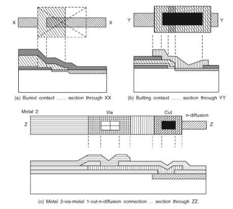
14 Via Rules: VIA is used to connect higher level metals from metal1 connection. Processes may vary in whether they allow stackedvias to be placed over polysilicon and diffusion regions. Some processes allow vias to be placed within these areas, but do not allow the vias to straddle the boundary of polysilicon or diffusion. Contact Cuts: While making contacts between poly-silicon and diffusion in nmos circuits it should be remembered that there are three possible approaches 1.poly to metal then metal to diff. 2. Buried contact poly to diff. 3. Butting contact (poly. to diff. using metal). Among the three the latter two, the buried contact is the most widely used, because of advantage in space and a reliable contact. At one time butting contacts were widely used, but now a days they are superseded by buried contacts. Other Rules: The passivation or overglass layer is a protective layer of Si02 (glass) that covers the final chip. Appropriately sized openings are required at pads and any internal test points. Some additional rules that might be present in some processes are as follows: Extension of polysilicon in the direction that metal wires exit a contact. Extension of metal end-of-line region beyond a via. Differing pmos and nmos gate lengths. Differing gate poly extensions depending on the device length or the device construction.
15

16 MOSIS Scalable CMOS Design Rules: Academic designs often use the λ-based scalable CMOS design rules from MOSIS because they are simple and freely available, and they allow designs to easily migrate from one process to another. These advantages come at the expense of being conservative because they must work for all manufacturing processes. MOSIS actually has three sets of rules: SCMOS, SUBM, and DEEP. The SUBM rules are somewhat more conservative than SCMOS rules. DEEP rules are even more conservative. The more conservative rules allow you to use a slightly smaller value of λ while still satisfying all of the micron design rules for a process. Table 2 lists some of the foundry processes MOSIS has offered and the associate value of λ for the different rule sets. For example, the AMI 0.5 µm process can use the SCMOS rules with λ = 0.35 µm or the SUBM rules with λ = 0.30 µm. SUBM rules are a good choice for class projects because they are somewhat easier to use than DEEP (no half-λ rules), while still being compatible with most processes. Some processes offer a second polysilicon layer for floating-gate transistors and poly-insulator-poly capacitors used in analog circuits. For design rules where the minimum drawn gate length exceeds the feature size, MOSIS applies a polysilicon bias to shrink the gates by a uniform amount before masks are made. For example, in the SUBM rules for the AMI 0.5 µm process with λ = 0.3 µm, a bias of- 0.1 µm is applied to all polysilicon. Thus, a 2 λ transistor gate is 0.5 µm rather than 0.6 µm and a 4 λ gate is 1.1 µm rather than 1.2 µm.


17 CMOS Lambda-based Design Rules: The CMOS fabrication process is more complex than nmos fabrication. In a CMOS process, there are nearly 100 actual set of industrial design rules. The additional rules are concerned with those features unique to p-well CMOS, such as the p-well and p+ mask and the special 'substrate' contacts. The p-well rules are shown in the diagram below. In the diagram above each of the arrangements can be merged into single split contacts. From the above diagram it is also clear that split contacts may also be made with separate cuts. Fig. Particular rules for p-well CMOS Process. The CMOS rules are designed based on the extensions of the Mead and Conway concepts and also by excluding the butting and buried contacts.

18 General Observations on the Design Rules: The microscopic dimensions of Silicon circuits always cause some problems in the design process. The major problem is presented by possible deviation in line widths and in interlayer registration. If the line widths are too small, it is possible for lines to be discontinuous in places. If separate paths in a layer are placed too close together, it is possible that they will merge in places or interfere with each other. For the lambda-based rules, the design rules are formulated in terms of a length unit λ which is related to the resolution of the process λ may be viewed as a limit on the width deviation of a feature from its ideal 'as drawn' size and also as a bound on the maximum misalignment of any one mask. In the worst case, these effects may combine to cause the relative position of feature edges on different mask levels to deviate by as much as 2λ in their interrelationship. Inevitably, a consequence of using the lambdabased concept is that every dimension must be rounded up to whole λ values and this leads to layouts which do not fully exploit the capabilities of the process. Similar concepts underlie the establishment of 'micron-based' rule sets, but actual dimensions are given so that full advantage can be taken of the fabrication line capabilities and tighter layouts result. Layout rules, therefore, provide strict guidelines for preparing the geometric layouts which will be used to configure the actual masks used during fabrication and can be regarded as the main communication link between circuit/systems designers and the process engineers engaged in manufacture. The goal of any set of design rules should give optimize yield while keeping the geometry as small as possible without compromising the reliability of the finished circuit. On the questions of yield and reliability, even the conservative nature of the lambda based rules can stand reevaluation when these two factors are of paramount importance. In particular, the rules associated with contacts can be improved upon in the light of experience. Fig.(a) sets out aspects that may be observed for high yield and in high reliability situations. In our proposed scheme of events in creating stick layouts for CMOS, it is assumed that poly and metal can both freely cross well boundaries and this is indeed the case, but we should be careful to try to exclude poly from areas which lie within p+ mask areas where possible. The reason for this is that the resistance of the poly. layer is reduced in current processes by n - type doping. Clearly the p+ doping which takes place inside the p+ mask will also dope the poly. which is already in place when the p+ doping step takes place. This results in an increase in the n - doping poly. resistance which may be significant in certain parts of a system.


19 The 3λ. metal width rule is a conservative one but is implemented to allow for the fact that the metal layer is deposited after the others and on top of them and several layers of silicon dioxide, so that the surface on which it sits is quite 'mountainous'. The metal layer is also light-reflective and these factors combine to result in poor edge definition. In double metal the second layer of metal has an even more uneven terrain on which to be deposited and patterned. Hence metal 2 is often wider than metal 1. Metal to metal separation is also large and is brought about mainly by difficulties in defining metal edges accurately during masking operations on the highly reflective metal. All diffusion processes are such that lateral diffusion occurs as well as impurity penetration from the surface. Hence the separation rules for diffusion allow for this and relatively large separations are specified. This is particularly the case for the p-well diffusions which are deep diffusions and thus have considerable lateral spread. Transitions from thin gate oxide to thick field oxide in the oxidation process also use up space and this is another reason why the lambda-based rules require a minimum separation between thinox regions of 3λ. In effect, this implies that the minimum feature size for thick oxide is 3λ.The simplicity of the lambda-based rules makes this approach to design an appropriate one for the novice chip designer and also, perhaps, for those applications in which we are not trying to achieve the absolute minimum area and the absolute maximum performance. Because lambda-based rules try 'to be all things to all people', they do suffer from least common denominator effects and from the upward rounding of all process line dimension parameters into integer values of lambda..

20

21 Orbit 2µm CMOS process: In this process all the spacing between each layers and dimensions will be in terms micrometer. The 2µm here represents the feature size. All the design rules whatever we have seen will not have lambda instead it will have the actual dimension in micrometer. In one way lambda based design rules are better compared micrometer based design rules, that is lambda based rules are feature size independent. Figure below shows the design rule for BiCMOS process using orbit 2um process.
22 Double metal MOS process rules: In the MOS design rules a powerful design process is achieved by adding a second metal layer. This gives a much greater degree of freedom, in distributing global VDD and Vss(GND) rails in a system. From the overall chip inter-connection aspect, the second metal layer in particular is important and, although the use of such a layer is readily envisaged, its disposition relative to its connection. To other layers using metal1 to metal 2 contacts, called vias, can be readily established. Usually, second level metal layers are coarser than the first (conventional) layer and the isolation layer between the layers may also be of relatively greater thickness. To distinguish contacts between first and second metal layers, they are known as vias rather than contact cuts. The second metal layer representation is color coded dark blue (or purple). The important process steps for a two-metal layer process are given below. The oxide below the first metal layer is deposited by atmospheric chemical vapor deposition (CVD) and the oxide layer between the metal layers is applied in a similar manner. Depending on the process, removal of selected areas of the oxide is accomplished by plasma etching, which is designed to have a high level of vertical ion bombardment to allow for high and uniform etch rates. Similarly, the bulk of the process steps for a double polysilicon layer process are similar in nature to those already described, except that a second thin oxide layer is grown after depositing and patterning the first polysilicon layer (Poly.1) to isolate it from the now to be deposited second poly. Layer (Poly.2). The presence of a second poly. Layer gives greater flexibility in interconnections and also allows Poly.2 transistors to be formed by intersecting Poly. 2 and diffusion. The important features of double metal process are summarized as follows: Use the second level metal for the global distribution of power buses, that is, VDD and GND (Vss), and for clock lines. Use the first level metal for local distribution of power and for signal lines. Lay out the two metal layers so that the conductors are mutually orthogonal wherever possible.
23 CMOS Inverter Layout : GND In V DD A A Out (a) Layout A A p-substrate n Field Oxide n + (b) Cross-Section along A-A p + VDD Contact Cut VDD X n-well x x x X X x X Gnd Gnd

24 Alternate Layout of NOT Gate : VDD VDD X X x x X X Gnd x Gnd x
25 NAND2 Layout: VDD VDD a.b X X X Gnd a b X X a.b NOR2 Layout : Gnd VDD a b VDD X X a b a b Gnd a b Gnd X X a b X TRANSMISSION GATE : Symbol schematic


26 stick diagram layout
27 Scaling of MOS Circuits: 1. What is Scaling? Proportional adjustment of the dimensions of an electronic device while maintaining the electrical properties of the device, results in a device either larger or smaller than the unscaled device. 2. Why Scaling? Scale the devices and wires down, Make the chips fatter functionality, intelligence, memory and faster, Make more chips per wafer increased yield, Make the end user Happy by giving more for less and therefore, make MORE MONEY!! Impact of scaling is characterized in terms of several indicators: Minimum feature size Number of gates on one chip Power dissipation Maximum operational frequency Die size Production cost Types of scaling: Scaling Models 1. Full Scaling (Constant Electrical Field): Ideal model dimensions and voltage scale together by the same scale factor. Requires to reduce power supply voltage with the reduction of feature size. The electric field across the gate-oxide does not change when the technology is scaled. 2. Fixed Voltage Scaling (Constant voltage scaling): Most common model until recently only the dimensions scale, voltages remain constant. Increasing electric field leads to velocity saturation, mobility degradation, and sub threshold leakage 3. General Scaling: Most realistic for today s situation voltages and dimensions scale with different factors Scaling Factors for Device Parameters Device scaling modeled in terms of generic scaling factors: 1/αand 1/β 1/β: scaling factor for supply voltage VDD, and gate oxide thickness D 1/α: linear dimensions both horizontal and vertical dimensions Why is the scaling factor for gate oxide thickness different from other linear horizontal and vertical dimensions? Consider the cross section of the device as in Figure 6, various parameters derived are as follows.
 Power Dissipation Per")
28 Limiting factors of scaling: 1) Hot Carrier Effect 2) Punch Through 3) Drain Induced Barrier Lowering (DIBL) 4) Gate Induced Barrier Lowering (GIBL) Gate Area Gate Capacitance per unit area Gate Capacitance Charge in Channel Channel Resistance Transistor Delay Maximum Operating Frequency Transistor Current Switching Energy Power Dissipation Per Gate (Static and Dynamic) Power Dissipation Per Unit Area Power - Speed Product
29
30
31 Implications of Scaling: Improved Performance Improved Cost Interconnect Woes Power Woes Productivity Challenges Physical Limits Limitations of Scaling Effects, as a result of scaling down- which eventually become severe enough to prevent further miniaturization. o o o o o o o Substrate doping Depletion width Limits of miniaturization Limits of interconnect and contact resistance Limits due to sub threshold currents Limits on logic levels and supply voltage due to noise Limits due to current density
32


33 OR 3-inputs, AND, then Inverter:


34 CMOS TG BASED 4 -INPUT MUX 1 BIT CMOS SHIFT REGISTER CELL

35 BICMOS 2 INPUT NAND GATE BICMOS 2 INPUT NOR GATE

36
Introduction to Layout design
 Introduction to Layout design Note: some figures are taken from Ref. B. Razavi, Design of Analog CMOS integrated circuits, Mc Graw-Hill, 001, and MOSIS web site: http://www.mosis.org/ 1 Introduction to
Lay ay ut Design g R ules
 HPTER 5: Layout esign Rules Introduction ny circuit physical mask layout must conform to a set of geometric constraints or rules called as Layout esign rules before it can be manufactured using particular
FABRICATION OF CMOS INTEGRATED CIRCUITS. Dr. Mohammed M. Farag
 FABRICATION OF CMOS INTEGRATED CIRCUITS Dr. Mohammed M. Farag Outline Overview of CMOS Fabrication Processes The CMOS Fabrication Process Flow Design Rules EE 432 VLSI Modeling and Design 2 CMOS Fabrication
Lecture 4a. CMOS Fabrication, Layout and Simulation. R. Saleh Dept. of ECE University of British Columbia
 Lecture 4a CMOS Fabrication, Layout and Simulation R. Saleh Dept. of ECE University of British Columbia res@ece.ubc.ca 1 Fabrication Fabrication is the process used to create devices and wires. Transistors
Circuits. L3: Fabrication and Layout -1 ( ) B. Mazhari Dept. of EE, IIT Kanpur. B. Mazhari, IITK. G-Number
 B. Mazhari Dept. of EE, IIT Kanpur. B. Mazhari, IITK. G-Number") EE60: CMOS Analog Circuits L: Fabrication and Layout - (8.8.0) B. Mazhari Dept. of EE, IIT Kanpur Suppose we have a Silicon wafer which is P-type and we wish to create a region within it which is N-type
EE60: CMOS Analog Circuits L: Fabrication and Layout - (8.8.0) B. Mazhari Dept. of EE, IIT Kanpur Suppose we have a Silicon wafer which is P-type and we wish to create a region within it which is N-type
Composite Layout CS/EE N-type from the top. N-type Transistor. Diffusion Mask. Polysilicon Mask
 Composite Layout CS/EE 6710 Introduction to Layout Inverter Layout Example Layout Design Rules Drawing the mask layers that will be used by the fabrication folks to make the devices Very different from
Process technology and introduction to physical
 Neuromorphic Engineering II Lab 3, Spring 2014 1 Lab 3 March 10, 2014 Process technology and introduction to physical layout Today you will start to learn to use the Virtuoso layout editor XL which is
Digital Integrated Circuits (83-313) Lecture 2: Technology and Standard Cell Layout
 Lecture 2: Technology and Standard Cell Layout") Digital Integrated Circuits (83-313) Lecture 2: Technology and Standard Cell Layout Semester B, 2016-17 Lecturer: Dr. Adam Teman TAs: Itamar Levi, Robert Giterman 26 March 2017 Disclaimer: This course
Digital Integrated Circuits (83-313) Lecture 2: Technology and Standard Cell Layout Semester B, 2016-17 Lecturer: Dr. Adam Teman TAs: Itamar Levi, Robert Giterman 26 March 2017 Disclaimer: This course
CMOS Process Flow. Layout CAD Tools
 CMOS Process Flow See supplementary power point file for animated CMOS process flow (see class ece410 website and/or* http://www.multimedia.vt.edu/ee5545/): This file should be viewed as a slide show It
Computer-Based Project on VLSI Design Co 3/7
 Computer-Based Project on VLSI Design Co 3/7 IC Layout and Symbolic Representation This pamphlet introduces the topic of IC layout in integrated circuit design and discusses the role of Design Rules and
VLSI Lab Tutorial 3. Virtuoso Layout Editing Introduction
 VLSI Lab Tutorial 3 Virtuoso Layout Editing Introduction 1.0 Introduction The purpose of this lab tutorial is to guide you through the design process in creating a custom IC layout for your CMOS inverter
ESE 570 Cadence Lab Assignment 2: Introduction to Spectre, Manual Layout Drawing and Post Layout Simulation (PLS)
") ESE 570 Cadence Lab Assignment 2: Introduction to Spectre, Manual Layout Drawing and Post Layout Simulation (PLS) Objective Part A: To become acquainted with Spectre (or HSpice) by simulating an inverter,
ESE 570 Cadence Lab Assignment 2: Introduction to Spectre, Manual Layout Drawing and Post Layout Simulation (PLS) Objective Part A: To become acquainted with Spectre (or HSpice) by simulating an inverter,
Digital Integrated CircuitDesign
 Digital Integrated CircuitDesign Lecture 8 Design Rules Adib Abrishamifar EE Department IUST Contents Design Rules CMOS Process Layers Intra-Layer Design Rules Via s and Contacts Select Layer Example Cell
Design rule illustrations for the AMI C5N process can be found at:
 Cadence Tutorial B: Layout, DRC, Extraction, and LVS Created for the MSU VLSI program by Professor A. Mason and the AMSaC lab group. Revised by C Young & Waqar A Qureshi -FS08 Document Contents Introduction
Chapter 2 On-Chip Protection Solution for Radio Frequency Integrated Circuits in Standard CMOS Process
 Chapter 2 On-Chip Protection Solution for Radio Frequency Integrated Circuits in Standard CMOS Process 2.1 Introduction Standard CMOS technologies have been increasingly used in RF IC applications mainly
CHAPTER 1 INTRODUCTION
 CHAPTER 1 INTRODUCTION Rapid advances in integrated circuit technology have made it possible to fabricate digital circuits with large number of devices on a single chip. The advantages of integrated circuits
CS310 Embedded Computer Systems. Maeng
 1 INTRODUCTION (PART II) Maeng Three key embedded system technologies 2 Technology A manner of accomplishing a task, especially using technical processes, methods, or knowledge Three key technologies for
3. Implementing Logic in CMOS
 3. Implementing Logic in CMOS 3. Implementing Logic in CMOS Jacob Abraham Department of Electrical and Computer Engineering The University of Texas at Austin VLSI Design Fall 27 September, 27 ECE Department,
CHAPTER 3 SIMULATION TOOLS AND
 CHAPTER 3 SIMULATION TOOLS AND Simulation tools used in this simulation project come mainly from Integrated Systems Engineering (ISE) and SYNOPSYS and are employed in different areas of study in the simulation
Schematic creation of MOS field effect transistor.
 Schematic creation of MOS field effect transistor. Gate electrode Drain electrode Source electrode Gate length Gate oxide A good reference is http://jas2.eng.buffalo.edu/applets/education/fab/nmos/nmos.html
Spiral 2-8. Cell Layout
 2-8.1 Spiral 2-8 Cell Layout 2-8.2 Learning Outcomes I understand how a digital circuit is composed of layers of materials forming transistors and wires I understand how each layer is expressed as geometric
MOSIS Scalable CMOS (SCMOS) Design Rules
 Design Rules") MOSIS Scalable CMOS (SCMOS) Design Rules (Revision 8.00) From : http://www.mosis.com/technical/designrules/scmos/scmos-main.html Updated: October 4, 2004 1. Introduction This document defines the official
MOSIS Scalable CMOS (SCMOS) Design Rules (Revision 8.00) From : http://www.mosis.com/technical/designrules/scmos/scmos-main.html Updated: October 4, 2004 1. Introduction This document defines the official
10. Interconnects in CMOS Technology
 10. Interconnects in CMOS Technology 1 10. Interconnects in CMOS Technology Jacob Abraham Department of Electrical and Computer Engineering The University of Texas at Austin VLSI Design Fall 2017 October
Process Technologies for SOCs
 UDC 621.3.049.771.14.006.1 Process Technologies for SOCs VTaiji Ema (Manuscript received November 30, 1999) This paper introduces a family of process technologies for fabriating high-performance SOCs.
Magic Technology Manual #1: NMOS
 Magic Technology Manual #1: NMOS John Ousterhout Computer Science Division Electrical Engineering and Computer Sciences University of California Berkeley, CA 970 (Warning: Process details often change.
EE 330 Laboratory 3 Layout, DRC, and LVS
 EE 330 Laboratory 3 Layout, DRC, and LVS Spring 2018 Contents Objective:... 2 Part 1 creating a layout... 2 1.1 Run DRC... 2 1.2 Stick Diagram to Physical Layer... 3 1.3 Bulk Connections... 3 1.4 Pins...
Introduction 1. GENERAL TRENDS. 1. The technology scale down DEEP SUBMICRON CMOS DESIGN
 1 Introduction The evolution of integrated circuit (IC) fabrication techniques is a unique fact in the history of modern industry. The improvements in terms of speed, density and cost have kept constant
Lab. Course Goals. Topics. What is VLSI design? What is an integrated circuit? VLSI Design Cycle. VLSI Design Automation
 Course Goals Lab Understand key components in VLSI designs Become familiar with design tools (Cadence) Understand design flows Understand behavioral, structural, and physical specifications Be able to
A Review Paper on Reconfigurable Techniques to Improve Critical Parameters of SRAM
 IJSRD - International Journal for Scientific Research & Development Vol. 4, Issue 09, 2016 ISSN (online): 2321-0613 A Review Paper on Reconfigurable Techniques to Improve Critical Parameters of SRAM Yogit
EE586 VLSI Design. Partha Pande School of EECS Washington State University
 EE586 VLSI Design Partha Pande School of EECS Washington State University pande@eecs.wsu.edu Lecture 1 (Introduction) Why is designing digital ICs different today than it was before? Will it change in
Integrated circuits and fabrication
 Integrated circuits and fabrication Motivation So far we have discussed about the various devices that are the heartbeat of core electronics. This modules aims at giving an overview of how these solid
Problem Formulation. Specialized algorithms are required for clock (and power nets) due to strict specifications for routing such nets.
 due to strict specifications for routing such nets.") Clock Routing Problem Formulation Specialized algorithms are required for clock (and power nets) due to strict specifications for routing such nets. Better to develop specialized routers for these nets.
Clock Routing Problem Formulation Specialized algorithms are required for clock (and power nets) due to strict specifications for routing such nets. Better to develop specialized routers for these nets.
EE 330 Laboratory 3 Layout, DRC, and LVS Fall 2015
 EE 330 Laboratory 3 Layout, DRC, and LVS Fall 2015 Contents Objective:... 2 Part 1 Creating a layout... 2 1.1 Run DRC Early and Often... 2 1.2 Create N active and connect the transistors... 3 1.3 Vias...
EE 330 Spring 2018 Laboratory 2: Basic Boolean Circuits
 EE 330 Spring 2018 Laboratory 2: Basic Boolean Circuits Contents Objective:... 2 Part 1: Introduction... 2 Part 2 Simulation of a CMOS Inverter... 3 Part 2.1 Attaching technology information... 3 Part
VLSI Test Technology and Reliability (ET4076)
") VLSI Test Technology and Reliability (ET4076) Lecture 8(2) I DDQ Current Testing (Chapter 13) Said Hamdioui Computer Engineering Lab Delft University of Technology 2009-2010 1 Learning aims Describe the
VLSI Test Technology and Reliability (ET4076) Lecture 8(2) I DDQ Current Testing (Chapter 13) Said Hamdioui Computer Engineering Lab Delft University of Technology 2009-2010 1 Learning aims Describe the
Power IC 용 ESD 보호기술. 구용서 ( Yong-Seo Koo ) Electronic Engineering Dankook University, Korea
 Electronic Engineering Dankook University, Korea") Power IC 용 ESD 보호기술 구용서 ( Yong-Seo Koo ) Electronic Engineering Dankook University, Korea yskoo@dankook.ac.kr 031-8005-3625 Outline Introduction Basic Concept of ESD Protection Circuit ESD Technology Issue
Power IC 용 ESD 보호기술 구용서 ( Yong-Seo Koo ) Electronic Engineering Dankook University, Korea yskoo@dankook.ac.kr 031-8005-3625 Outline Introduction Basic Concept of ESD Protection Circuit ESD Technology Issue
Cluster-based approach eases clock tree synthesis
 Page 1 of 5 EE Times: Design News Cluster-based approach eases clock tree synthesis Udhaya Kumar (11/14/2005 9:00 AM EST) URL: http://www.eetimes.com/showarticle.jhtml?articleid=173601961 Clock network
Low-Power Technology for Image-Processing LSIs
 Low- Technology for Image-Processing LSIs Yoshimi Asada The conventional LSI design assumed power would be supplied uniformly to all parts of an LSI. For a design with multiple supply voltages and a power
QUESTION BANK DEPARTMENT OF ECE
 QUESTION BANK DEPARTMENT OF ECE YEAR: III SEM: VI SUBJECTCODE:EC2354 SUBJECT NAME:VLSI DESIGN Prepared by V.GUNASUNDARI/AP 1.List the advantages of SOI CMOS process Denser transistor structures are possible.
Cadence Virtuoso Schematic Design and Circuit Simulation Tutorial
 Cadence Virtuoso Schematic Design and Circuit Simulation Tutorial Introduction This tutorial is an introduction to schematic capture and circuit simulation for ENGN1600 using Cadence Virtuoso. These courses
UNIT IV CMOS TESTING
 UNIT IV CMOS TESTING 1. Mention the levels at which testing of a chip can be done? At the wafer level At the packaged-chip level At the board level At the system level In the field 2. What is meant by
CMOS INVERTER LAYOUT TUTORIAL
 PRINCESS SUMAYA UNIVERSITY FOR TECHNOLOGY CMOS INVERTER LAYOUT TUTORIAL We will start the inverter by drawing a PMOS. The first step is to draw a poly layer. Click on draw a rectangle and choose the poly
SIDDHARTH INSTITUTE OF ENGINEERING AND TECHNOLOGY :: PUTTUR (AUTONOMOUS) Siddharth Nagar, Narayanavanam Road QUESTION BANK UNIT I
 Siddharth Nagar, Narayanavanam Road QUESTION BANK UNIT I") SIDDHARTH INSTITUTE OF ENGINEERING AND TECHNOLOGY :: PUTTUR (AUTONOMOUS) Siddharth Nagar, Narayanavanam Road 517583 QUESTION BANK Subject with Code : DICD (16EC5703) Year & Sem: I-M.Tech & I-Sem Course
SIDDHARTH INSTITUTE OF ENGINEERING AND TECHNOLOGY :: PUTTUR (AUTONOMOUS) Siddharth Nagar, Narayanavanam Road 517583 QUESTION BANK Subject with Code : DICD (16EC5703) Year & Sem: I-M.Tech & I-Sem Course
UNIVERSITY OF CALIFORNIA College of Engineering Department of Electrical Engineering and Computer Sciences Lab #2: Layout and Simulation
 UNIVERSITY OF CALIFORNIA College of Engineering Department of Electrical Engineering and Computer Sciences Lab #2: Layout and Simulation NTU IC541CA 1 Assumed Knowledge This lab assumes use of the Electric
Design Methodologies
 Design Methodologies 1981 1983 1985 1987 1989 1991 1993 1995 1997 1999 2001 2003 2005 2007 2009 Complexity Productivity (K) Trans./Staff - Mo. Productivity Trends Logic Transistor per Chip (M) 10,000 0.1
FPGA Programming Technology
 FPGA Programming Technology Static RAM: This Xilinx SRAM configuration cell is constructed from two cross-coupled inverters and uses a standard CMOS process. The configuration cell drives the gates of
TABLE OF CONTENTS 1.0 PURPOSE INTRODUCTION ESD CHECKS THROUGHOUT IC DESIGN FLOW... 2
 TABLE OF CONTENTS 1.0 PURPOSE... 1 2.0 INTRODUCTION... 1 3.0 ESD CHECKS THROUGHOUT IC DESIGN FLOW... 2 3.1 PRODUCT DEFINITION PHASE... 3 3.2 CHIP ARCHITECTURE PHASE... 4 3.3 MODULE AND FULL IC DESIGN PHASE...
Introduction to ICs and Transistor Fundamentals
 Introduction to ICs and Transistor Fundamentals A Brief History 1958: First integrated circuit Flip-flop using two transistors Built by Jack Kilby at Texas Instruments 2003 Intel Pentium 4 mprocessor (55
Virtuoso Layout Editor
 This tutorial will cover the basic steps involved in using the Cadence layout editor called Virtuoso, extracting layout, and running simulation on the layout. The inverter layout is used as an example
EE 330 Spring Laboratory 2: Basic Boolean Circuits
 EE 330 Spring 2013 Laboratory 2: Basic Boolean Circuits Objective: The objective of this experiment is to investigate methods for evaluating the performance of Boolean circuits. Emphasis will be placed
Cell Libraries and Design Hierarchy. Instructor S. Demlow ECE 410 February 1, 2012
 Cell Libraries and Design Hierarchy Instructor S. Demlow ECE 410 February 1, 2012 Stick Diagrams Simplified NAND Layout Simplified NOR Layout Metal supply rails blue n and p Active green Poly gates red
VLSI Test Technology and Reliability (ET4076)
") VLSI Test Technology and Reliability (ET4076) Lecture 4(part 2) Testability Measurements (Chapter 6) Said Hamdioui Computer Engineering Lab Delft University of Technology 2009-2010 1 Previous lecture What
VLSI Test Technology and Reliability (ET4076) Lecture 4(part 2) Testability Measurements (Chapter 6) Said Hamdioui Computer Engineering Lab Delft University of Technology 2009-2010 1 Previous lecture What
Chapter 5: ASICs Vs. PLDs
 Chapter 5: ASICs Vs. PLDs 5.1 Introduction A general definition of the term Application Specific Integrated Circuit (ASIC) is virtually every type of chip that is designed to perform a dedicated task.
Latch-Up. Parasitic Bipolar Transistors
 Latch-Up LATCH-UP CIRCUIT Latch-up is caused by an SCR (Silicon Controlled Rectifier) circuit. Fabrication of CMOS integrated circuits with bulk silicon processing creates a parasitic SCR structure. The
Cadence Tutorial 2: Layout, DRC/LVS and Circuit Simulation with Extracted Parasitics
 Cadence Tutorial 2: Layout, DRC/LVS and Circuit Simulation with Extracted Parasitics Introduction This tutorial describes how to generate a mask layout in the Cadence Virtuoso Layout Editor. Use of DIVA
ENEE 359a Digital VLSI Design
 SLIDE 1 ENEE 359a Digital VLSI Design Course : Transistors to Systems Prof. blj@eng.umd.edu Credit where credit is due: Slides contain original artwork ( Jacob 2004) as well as material taken liberally
IMPLEMENTATION OF LOW POWER AREA EFFICIENT ALU WITH LOW POWER FULL ADDER USING MICROWIND DSCH3
 IMPLEMENTATION OF LOW POWER AREA EFFICIENT ALU WITH LOW POWER FULL ADDER USING MICROWIND DSCH3 Ritafaria D 1, Thallapalli Saibaba 2 Assistant Professor, CJITS, Janagoan, T.S, India Abstract In this paper
EE115C Digital Electronic Circuits. Tutorial 4: Schematic-driven Layout (Virtuoso XL)
") EE115C Digital Electronic Circuits Tutorial 4: Schematic-driven Layout (Virtuoso XL) This tutorial will demonstrate schematic-driven layout on the example of a 2-input NAND gate. Simple Layout (that won
EE115C Digital Electronic Circuits Tutorial 4: Schematic-driven Layout (Virtuoso XL) This tutorial will demonstrate schematic-driven layout on the example of a 2-input NAND gate. Simple Layout (that won
11 Patent Number: 5,519,242 Avery 45) Date of Patent: May 21, 1996
 Date of Patent: May 21, 1996") United States Patent (19) I I USOO5519242A 11 Patent Number: 5,519,242 Avery 45) Date of Patent: May 21, 1996 54 ELECTROSTATIC DISCHARGE 5,357,126 10/1994 Jimenez... 257/173 PROTECTION CIRCUIT FOR A NMOS
United States Patent (19) I I USOO5519242A 11 Patent Number: 5,519,242 Avery 45) Date of Patent: May 21, 1996 54 ELECTROSTATIC DISCHARGE 5,357,126 10/1994 Jimenez... 257/173 PROTECTION CIRCUIT FOR A NMOS
CMOS TECHNOLOGY- Chapter 2 in the Text
 CMOS TECHOLOGY- Chapter 2 in the Text CMOS Technology- Chapter 2 We will describe a modern CMOS process flow. In the simplest CMOS technologies, we need to realize simply MOS and MOS transistors for circuits
When it comes to double-density Flash memory, some pairs are just better.
 MirrorBit Flash When it comes to double-density Flash memory, some pairs are just better. AMD pairs high-performance with reliability in a single Flash memory cell, with revolutionary results. Introducing
Sketch A Transistor-level Schematic Of A Cmos 3-input Xor Gate
 Sketch A Transistor-level Schematic Of A Cmos 3-input Xor Gate DE09 DIGITALS ELECTRONICS 3 (For Mod-m Counter, we need N flip-flops (High speeds are possible in ECL because the transistors are used in
Memory Design I. Array-Structured Memory Architecture. Professor Chris H. Kim. Dept. of ECE.
 Memory Design I Professor Chris H. Kim University of Minnesota Dept. of ECE chriskim@ece.umn.edu Array-Structured Memory Architecture 2 1 Semiconductor Memory Classification Read-Write Wi Memory Non-Volatile
3D systems-on-chip. A clever partitioning of circuits to improve area, cost, power and performance. The 3D technology landscape
 Edition April 2017 Semiconductor technology & processing 3D systems-on-chip A clever partitioning of circuits to improve area, cost, power and performance. In recent years, the technology of 3D integration
+1 (479)
") Memory Courtesy of Dr. Daehyun Lim@WSU, Dr. Harris@HMC, Dr. Shmuel Wimer@BIU and Dr. Choi@PSU http://csce.uark.edu +1 (479) 575-6043 yrpeng@uark.edu Memory Arrays Memory Arrays Random Access Memory Serial
Memory Courtesy of Dr. Daehyun Lim@WSU, Dr. Harris@HMC, Dr. Shmuel Wimer@BIU and Dr. Choi@PSU http://csce.uark.edu +1 (479) 575-6043 yrpeng@uark.edu Memory Arrays Memory Arrays Random Access Memory Serial
Full Custom Layout Optimization Using Minimum distance rule, Jogs and Depletion sharing
 Full Custom Layout Optimization Using Minimum distance rule, Jogs and Depletion sharing Umadevi.S #1, Vigneswaran.T #2 # Assistant Professor [Sr], School of Electronics Engineering, VIT University, Vandalur-
Digital Integrated Circuits A Design Perspective. Jan M. Rabaey
 Digital Integrated Circuits A Design Perspective Jan M. Rabaey Outline (approximate) Introduction and Motivation The VLSI Design Process Details of the MOS Transistor Device Fabrication Design Rules CMOS
Chapter 6. CMOS Functional Cells
 Chapter 6 CMOS Functional Cells In the previous chapter we discussed methods of designing layout of logic gates and building blocks like transmission gates, multiplexers and tri-state inverters. In this
Integrated Circuits & Systems
 Federal University of Santa Catarina Center for Technology Computer Science & Electronics Engineering Integrated Circuits & Systems INE 5442 Lecture 23-1 guntzel@inf.ufsc.br Semiconductor Memory Classification
ESE570 Spring University of Pennsylvania Department of Electrical and System Engineering Digital Integrated Cicruits AND VLSI Fundamentals
 University of Pennsylvania Department of Electrical and System Engineering Digital Integrated Cicruits AND VLSI Fundamentals ESE570, Spring 2019 HW5: Delay and Layout Sunday, February 17th Due: Friday,
TUTORIAL II ECE 555 / 755 Updated on September 11 th 2006 CADENCE LAYOUT AND PARASITIC EXTRACTION
 TUTORIAL II ECE 555 / 755 Updated on September 11 th 2006 CADENCE LAYOUT AND PARASITIC EXTRACTION After finishing a schematic of your design (Tutorial-I), the next step is creating masks which are for
Chapter 1 Introduction
 Chapter 1 Introduction 1.1 MOTIVATION 1.1.1 LCD Industry and LTPS Technology [1], [2] The liquid-crystal display (LCD) industry has shown rapid growth in five market areas, namely, notebook computers,
Embedded SRAM Technology for High-End Processors
 Embedded SRAM Technology for High-End Processors Hiroshi Nakadai Gaku Ito Toshiyuki Uetake Fujitsu is the only company in Japan that develops its own processors for use in server products that support
Design Compiler Graphical Create a Better Starting Point for Faster Physical Implementation
 Datasheet Create a Better Starting Point for Faster Physical Implementation Overview Continuing the trend of delivering innovative synthesis technology, Design Compiler Graphical streamlines the flow for
Linear Regression and Random Forests for Layer Identification in IC Layout Reverse-Engineering
 000 001 002 003 004 005 006 007 008 009 010 011 012 013 014 015 016 017 018 019 020 021 022 023 024 025 026 027 028 029 030 031 032 033 034 035 036 037 038 039 040 041 042 043 044 045 046 047 048 049 050
Power Consumption in 65 nm FPGAs
 White Paper: Virtex-5 FPGAs R WP246 (v1.2) February 1, 2007 Power Consumption in 65 nm FPGAs By: Derek Curd With the introduction of the Virtex -5 family, Xilinx is once again leading the charge to deliver
A Novel Methodology to Debug Leakage Power Issues in Silicon- A Mobile SoC Ramp Production Case Study
 A Novel Methodology to Debug Leakage Power Issues in Silicon- A Mobile SoC Ramp Production Case Study Ravi Arora Co-Founder & CTO, Graphene Semiconductors India Pvt Ltd, India ABSTRACT: As the world is
Very Large Scale Integration (VLSI)
") Very Large Scale Integration (VLSI) Lecture 8 Dr. Ahmed H. Madian ah_madian@hotmail.com Content Array Subsystems Introduction General memory array architecture SRAM (6-T cell) CAM Read only memory Introduction
Very Large Scale Integration (VLSI) Lecture 8 Dr. Ahmed H. Madian ah_madian@hotmail.com Content Array Subsystems Introduction General memory array architecture SRAM (6-T cell) CAM Read only memory Introduction
Pad Ring and Floor Planning
 Pad Ring and Floor Planning Pad Ring Core Block 1 Block 2 Block Block 3 Block 6 Block 5 The core of the chip (made up of one or more top level blocks) is surrounded by a ring of pads. The design of the
CHAPTER 12 ARRAY SUBSYSTEMS [ ] MANJARI S. KULKARNI
![CHAPTER 12 ARRAY SUBSYSTEMS [ ] MANJARI S. KULKARNI](/thumbs/76/73997056.jpg "CHAPTER 12 ARRAY SUBSYSTEMS [ ] MANJARI S. KULKARNI") CHAPTER 2 ARRAY SUBSYSTEMS [2.4-2.9] MANJARI S. KULKARNI OVERVIEW Array classification Non volatile memory Design and Layout Read-Only Memory (ROM) Pseudo nmos and NAND ROMs Programmable ROMS PROMS, EPROMs,
CHAPTER 2 ARRAY SUBSYSTEMS [2.4-2.9] MANJARI S. KULKARNI OVERVIEW Array classification Non volatile memory Design and Layout Read-Only Memory (ROM) Pseudo nmos and NAND ROMs Programmable ROMS PROMS, EPROMs,
VERY large scale integration (VLSI) design for power
 design for power") IEEE TRANSACTIONS ON VERY LARGE SCALE INTEGRATION (VLSI) SYSTEMS, VOL. 7, NO. 1, MARCH 1999 25 Short Papers Segmented Bus Design for Low-Power Systems J. Y. Chen, W. B. Jone, Member, IEEE, J. S. Wang,
IEEE TRANSACTIONS ON VERY LARGE SCALE INTEGRATION (VLSI) SYSTEMS, VOL. 7, NO. 1, MARCH 1999 25 Short Papers Segmented Bus Design for Low-Power Systems J. Y. Chen, W. B. Jone, Member, IEEE, J. S. Wang,
ASIC Physical Design Top-Level Chip Layout
 ASIC Physical Design Top-Level Chip Layout References: M. Smith, Application Specific Integrated Circuits, Chap. 16 Cadence Virtuoso User Manual Top-level IC design process Typically done before individual
Very Large Scale Integration (VLSI)
") Very Large Scale Integration (VLSI) Lecture 10 Dr. Ahmed H. Madian Ah_madian@hotmail.com Dr. Ahmed H. Madian-VLSI 1 Content Manufacturing Defects Wafer defects Chip defects Board defects system defects
Very Large Scale Integration (VLSI) Lecture 10 Dr. Ahmed H. Madian Ah_madian@hotmail.com Dr. Ahmed H. Madian-VLSI 1 Content Manufacturing Defects Wafer defects Chip defects Board defects system defects
CMOS VLSI DESIGN ROCHESTER INSTITUTE OF TECHNOLOGY MICROELECTRONIC ENGINEERING CMOS VLSI DESIGN. Dr. Lynn Fuller
 ROCHESTER INSTITUTE OF TECHNOLOGY MICROELECTRONIC ENGINEERING CMOS VLSI DESIGN Dr. Lynn Fuller Webpage: http://people.rit.edu/~lffeee 82 Lomb Memorial Drive Rochester, NY 14623-5604 Tel (585) 475-2035
FPGA Power Management and Modeling Techniques
 FPGA Power Management and Modeling Techniques WP-01044-2.0 White Paper This white paper discusses the major challenges associated with accurately predicting power consumption in FPGAs, namely, obtaining
ESD Protection Design for Mixed-Voltage I/O Interfaces -- Overview
 ESD Protection Design for Mixed-Voltage Interfaces -- Overview Ming-Dou Ker and Kun-Hsien Lin Abstract Electrostatic discharge (ESD) protection design for mixed-voltage interfaces has been one of the key
VLSI Design Automation
 943/U0220 & #901/60010 VLSI Design Automation 張耀文 Yao-Wen Chang ywchang@cc.ee.ntu.edu.tw http://cc.ee.ntu.edu.tw/~ywchang Graduate Institute of Electronics Engineering Department of Electrical Engineering
SIDDHARTH INSTITUTE OF ENGINEERING AND TECHNOLOGY :: PUTTUR (AUTONOMOUS) Siddharth Nagar, Narayanavanam Road QUESTION BANK
 Siddharth Nagar, Narayanavanam Road QUESTION BANK") SIDDHARTH INSTITUTE OF ENGINEERING AND TECHNOLOGY :: PUTTUR (AUTONOMOUS) Siddharth Nagar, Narayanavanam Road 517583 QUESTION BANK Subject with Code :VLSI Technology(16EC5701) Course & Branch: M.Tech (ES,
SIDDHARTH INSTITUTE OF ENGINEERING AND TECHNOLOGY :: PUTTUR (AUTONOMOUS) Siddharth Nagar, Narayanavanam Road 517583 QUESTION BANK Subject with Code :VLSI Technology(16EC5701) Course & Branch: M.Tech (ES,
More Course Information
 More Course Information Labs and lectures are both important Labs: cover more on hands-on design/tool/flow issues Lectures: important in terms of basic concepts and fundamentals Do well in labs Do well
CAD for VLSI. Debdeep Mukhopadhyay IIT Madras
 CAD for VLSI Debdeep Mukhopadhyay IIT Madras Tentative Syllabus Overall perspective of VLSI Design MOS switch and CMOS, MOS based logic design, the CMOS logic styles, Pass Transistors Introduction to Verilog
ΔΙΑΛΕΞΗ 5: FPGA Programming Technologies (aka: how to connect/disconnect wires/gates)
") ΗΜΥ 408 ΨΗΦΙΑΚΟΣ ΣΧΕΔΙΑΣΜΟΣ ΜΕ FPGAs Χειμερινό Εξάμηνο 2018 ΔΙΑΛΕΞΗ 5: FPGA Programming Technologies (aka: how to connect/disconnect wires/gates) (ack: Jurriaan Schmitz, Semiconductor Components) ΧΑΡΗΣ
ΗΜΥ 408 ΨΗΦΙΑΚΟΣ ΣΧΕΔΙΑΣΜΟΣ ΜΕ FPGAs Χειμερινό Εξάμηνο 2018 ΔΙΑΛΕΞΗ 5: FPGA Programming Technologies (aka: how to connect/disconnect wires/gates) (ack: Jurriaan Schmitz, Semiconductor Components) ΧΑΡΗΣ
VLSI Test Technology and Reliability (ET4076)
") VLSI Test Technology and Reliability (ET4076) Lecture 2 (p2) Fault Modeling (Chapter 4) Said Hamdioui Computer Engineering Lab Delft University of Technology 2009-2010 1 Previous lecture What are the different
VLSI Test Technology and Reliability (ET4076) Lecture 2 (p2) Fault Modeling (Chapter 4) Said Hamdioui Computer Engineering Lab Delft University of Technology 2009-2010 1 Previous lecture What are the different
UNIT 4 INTEGRATED CIRCUIT DESIGN METHODOLOGY E5163
 UNIT 4 INTEGRATED CIRCUIT DESIGN METHODOLOGY E5163 LEARNING OUTCOMES 4.1 DESIGN METHODOLOGY By the end of this unit, student should be able to: 1. Explain the design methodology for integrated circuit.
Memory. Outline. ECEN454 Digital Integrated Circuit Design. Memory Arrays. SRAM Architecture DRAM. Serial Access Memories ROM
 ECEN454 Digital Integrated Circuit Design Memory ECEN 454 Memory Arrays SRAM Architecture SRAM Cell Decoders Column Circuitry Multiple Ports DRAM Outline Serial Access Memories ROM ECEN 454 12.2 1 Memory
ECE 261: Full Custom VLSI Design
 ECE 261: Full Custom VLSI Design Prof. James Morizio Dept. Electrical and Computer Engineering Hudson Hall Ph: 201-7759 E-mail: jmorizio@ee.duke.edu URL: http://www.ee.duke.edu/~jmorizio Course URL: http://www.ee.duke.edu/~jmorizio/ece261/261.html
Chip/Package/Board Design Flow
 Chip/Package/Board Design Flow EM Simulation Advances in ADS 2011.10 1 EM Simulation Advances in ADS2011.10 Agilent EEsof Chip/Package/Board Design Flow 2 RF Chip/Package/Board Design Industry Trends Increasing
Digital Design Methodology (Revisited) Design Methodology: Big Picture
 Design Methodology: Big Picture") Digital Design Methodology (Revisited) Design Methodology Design Specification Verification Synthesis Technology Options Full Custom VLSI Standard Cell ASIC FPGA CS 150 Fall 2005 - Lec #25 Design Methodology
Digital Design Methodology (Revisited) Design Methodology Design Specification Verification Synthesis Technology Options Full Custom VLSI Standard Cell ASIC FPGA CS 150 Fall 2005 - Lec #25 Design Methodology
Analog and Telecommunication Electronics
 Politecnico di Torino Electronic Eng. Master Degree Analog and Telecommunication Electronics F2 Active power devices»mos»bjt» IGBT, TRIAC» Safe Operating Area» Thermal analysis AY 2015-16 26/04/2016-1
MAGIC TUTORIAL. Getting Started: Background Info: RLW 10/15/98 3:12 PM
 MAGIC TUTORIAL Getting Started: Login to one of the workstations located in ECEE 253 using login name iclab. There is no password so just hit [enter]. The local directory on each machine is /home/sp98/iclab.
Digital Design Methodology
 Digital Design Methodology Prof. Soo-Ik Chae Digital System Designs and Practices Using Verilog HDL and FPGAs @ 2008, John Wiley 1-1 Digital Design Methodology (Added) Design Methodology Design Specification