EE251: Tuesday December 4
|
|
|
- Mercy Phillips
- 5 years ago
- Views:
Transcription
1 EE251: Tuesday December 4 Memory Subsystem continued Timing requirements Adding memory beyond 4 Gbyte Time Allowing: Begin Review for Final Exam Homework #9 due Thursday at beginning of class Friday is deadline for all labs; all labs required! Practical Exam #2 is this week during lab. See website. Final Exam on Monday, Dec 10, 2:00 pm. 90 minute exam Final Review on Sunday, Dec. 9 at 6 pm in ENGR 120 Two sided sheet with handwritten notes allowed and encouraged Calculator (Hex OK) allowed and encouraged Pencils and eraser HIGHLY encouraged Lecture #28 1
2 Practical # 2 There are 6 different labs; each has its own different practical exam But these exams aren t very different Therefore it is critical that you not share what was on your practical with anyone else until all practicals are complete, and don t ask others to share with you There have been an few problems with this in the past, and the consequences for those sharing have been very real Do your best on your own, and depend on some partial credit for what you do accomplish on your own. Questions? Lecture #28 2
3 TM4C Development Board The TM4C Development Board which was provided for your use at the beginning of the semester is YOURS! Part of your course fee this semester. No need to return it to anyone--i won t be around on Friday the 7 th as I said I would. Sorry about the confusion I just learned Thursday that these were part of your course fee. Enjoy your board! Teach it lots of fun tricks! Lecture #28 3
4 Expanding Memory Can expand physical memory beyond what s included on chip, within processor s address space. Some Design Requirements for adding memory: Maintain unique address for each memory location (data stored only once). The data bus is properly connected to all memory chips. Control lines are routed to appropriate pins on each memory chip. External memory chips are electrically compatible with our processor. Timing: This is the most complex part of expanding memory AND you need to grasp the concept. Lecture #28 4
5 Memory Timing Analysis Read Cycle A valid address is placed on address lines, guaranteed by rising edge of ECLK (external version of clock) Who guarantees this? (Hint: who creates address signal?) Control signals (ECLK and R/W) are issued to provide control signals to the memory (CS,OE) while ECLK is high Who provides these control signals? Data is read from the external memory must be there before falling edge of ECLK (details soon) Who assures data is there? (Hint: from the external memory ) Lecture #28 5
6 Memory Read Timing Diagram ADDR[31:0] DATA[7:0] R/W* All signals are provided by the CPU, except DATA[7:0]. Lecture #28 6
7 Read Data Setup Time Valid data will be available on the data pins after ALL the following RAM chip timing conditions have been satisfied: t ADDR (address access time): is defined as the time delay between when a valid address is provided to memory and when valid data is provided by memory. t CS (chip select access time): is defined as the time delay between when a valid Chip Select (CS*) is provided to memory and when valid data is provided by memory. t OE (output enable access time): is defined as the time delay between when a valid Output Enable (OE*) is provided to memory and when valid data is provided by memory. When we refer to (for example) a 15 ns RAM, we usually mean the address access time, t ADDR. That is because this is usually the determining speed factor of the three above. Lecture #28 7
8 Read Timing Signals RAM Chip Lecture #28 8
9 Typical Read Timing Signals t DHR E clock low t DSR E clock high After all the control signals are asserted and data is provided by the memory, data is read by the processor. However, a proper amount of read data hold time (t DHR ) and read data set-up time (t DSR ) must be followed for a proper data read operation. Read Data Hold time (t DHR ) : Specifies how long the data must remain valid after the falling edge of ECLK. Read Data Set-up time (t DSR ) : specifies how long the data must be present before the falling edge of ECLK. Lecture #28 9
10 Combined Read Timing Requirements T Eclock t else t dsr E clock low E clock high Addr valid Data valid ½T Eclock All memory signals must come true during high level of E clock. Therefore: CS--must have: logic to chip select + t cs + t dsr < 1/2 CPU Cycle Time = T Eclock /2 Or: logic to chip select + t cs < t else where t else = T Eclock /2 - t dsr Address--must have: t addr < t else Output Enable--must have: t NAND + t OE < t else Lecture #28 10
11 Read Timing Requirements Example t else = ½T Eclock t dsr logic to chip select + t cs < t else t addr < t else t NAND + t OE < t else Assume 10 MHz Bus Clock External chip assumptions: NAND gate has 8 ns. delay 3-8 decoder takes 23 ns. from any input Assume no logic to decoder enable lines Processor: t dsr = 19 ns. Memory Chip: t cs = 17 ns. t addr = 35 ns. t OE = 22 ns. SOLUTION: 10 MHz bus clock => T Eclock = 100 ns t else = ½T Eclock t dsr t else = 50 ns 19 ns = 31 ns logic to chip select + t cs < t else 23 ns + 17 ns = 40 ns <? 31 ns NO t addr < t else 35 ns <? 31 ns NO t NAND + t OE < t else 8 ns + 22 ns = 30 ns <? 31 ns YES Lecture #28 11
12 Another Read Timing Example t else = ½T Eclock t dsr logic to chip select + t cs < t else t addr < t else t NAND + t OE < t else Assume 8.33 MHz Bus Clock External chip assumptions: NAND gate has 10 ns. delay 3-8 decoder takes 25 ns. from any input Assume no logic to decoder enable lines Processor: t dsr = 25 ns. Memory Chip: t cs = 20 ns. t addr = 32 ns. t OE = 24 ns. SOLUTION: 8.33 MHz bus clock => T Eclock = 120 ns t else = ½T Eclock t dsr t else = 60 ns 25ns = 35 ns logic to chip select + t cs < t else 25 ns + 20 ns = 45 ns t addr < t else 32 ns t NAND + t OE < t else 10 ns + 24 ns = 34 ns Lecture #28 12
13 Example Write Cycle and Timing The write cycle consists of the following: 1. Control signals are issued by the CPU before ECLK rising edge. 2. CPU places address on the address lines ADDR[15:0] by ECLK. 3. CPU places data on the Data lines DATA[15:0] after ECLK. 4. Data is written into the desired memory location. All signals are provided by the processor. Lecture #28 13
14 Write Cycle Timing for RAM Chip The timing constraints for the write cycle is dictated by the properties of the memory unit (RAM). Hence, the memory data sheet would specify these constraints. Below is the brief description of the constraints t AS (Address Setup Time) : The address lines must be stable for a period of t AS time before the control signals are asserted (CS and WE) t AH (Address Hold time): The address lines must be held for a period of t AH (ns) after the control lines de-asserted. t CSW (Chip Select setup): CS line must be asserted t CSW (ns) before the end of the write cycle t WP (write pulse width) :The write enable control signal must stay asserted at least this long for a proper write t DS (Data Setup time): Data input lines must be stable at least t DS ns before the write cycle ends. t DH (Data Hold Time): All data inputs must be held stable until this time after the write cycle ends. Lecture #28 14
15 Combined Write Timing Requirements T Eclock ½T Eclock Supplied by Processor ECLK ADDR Bus DATA Bus E clock low E clock high Addr valid Data valid R/W* t DS CS* t CSW WE* t WP More signals to analyze on write cycle vs read: T as : address setup (address true before CS* and WE* activated), usually 0 ns. T csw : chip select setup before end of WE* pulse. A key parameter T wp : width of write pulse (WE*). Also a key parameter T ds : data valid before end of write. Another key parameter T dh : data true after end of write. Usually 0 ns. Lecture #28 15
16 Memory Expansion The memory of the most computer architectures can be expanded BEYOND their addressable memory space. This is done using a technology called Memory Paging, and is a common technique for microprocessors (including the Intel X86 architecture). The following slides will describe how it is done in the HCS12 Architecture as an example. This processor was used in ECE 251 before the TM4C. Some ARM processors, but not ours, allow memory paging. Lecture #28 16
17 Memory Paging Memory paging is concept in which a portion of the large memory can be accessed through a fixed window. This is analogous to a opening a page in the book and accessing only the information contained on the page. In this case, all the words in the book constitute our whole memory, and by referring to page numbers, we can have an access to the entire book, page by page. Some versions of the HCS12 have one memory expansion window, controlled by register PPAGE(0x30) whose use is described on the following slide. Lecture #28 17
18 Memory Paging Diagram Up to Page 63 The HCS12 Core architecture limits the physical address space available to 64K bytes. The Program Page Index Register allows for integrating up to 1M byte of FLASH or ROM into the system by using the six page index bits (PIX5:PIX0 of PPAGE) to page 64 16K byte blocks into the Program Page Window located between $8000 and $BFFF. Lecture #28 18
19 Program Page Index Register Bits These page index bits are used to select which of the 64 FLASH or ROM array pages is to be accessed in the Program Page Window as shown below: Lecture #28 19
20 Physical Memory Addressing Given this address space architecture, how much ROM/Flash memory can be addressed? 16K 64 = KBytes = MBytes So how many address lines must go to this physical flash memory if it is fully loaded? 2 to what power is the number above? So the physical address lines to this subsystem include 14 address lines (addr[13:0]) for each page and 6 extended address lines (Pix[5:0]). Other versions of this processor also allow mapped RAM to extend the amount of R/W memory in the system. Lecture #28 20
21 ECE 251 Final Exam Review Closed Book. Calculator OK. Ruler recommended. Appropriate Reference Two sides of one page handwritten notes OK. Documents will be provided. Topics Mostly Since Mid-Term Exam Ports Port Registers RCGCGPIO, DATA, DIR, DEN PUR, PDR, AFSEL Memory Mapped I/O Parallel I/O Input from Ports Output to Ports Switch Input Keypad Input LED Output 7 Segment Displays TIVA I/O Devices Buffers, esp. tristate I/O Programming Bit-Specific Addressing Delay Loops Polling vs. Interrupt Exceptions Reset Faults Interrupts Action upon Interrupt ISRs Turn on-off Interrupt Conditions Interrupt Handling Processor Action Register Stacking Programmer Action Use of Link Register (LR) Interrupt Vector Map Priority IRQ* Interrupt Line ISR Examples Fixed-point Arithmetic Floating-point Arithmetic Real-Time Module SysTick Phase Lock Loop Interrupts on fixed interval Engineering Notation Instruction Encoding/Decoding Timer Module GPTM Timer Clock Period, Frequency, Duty Cycle Input Capture Output-Compare Pulse Count I/O Pins via AFSEL Various GPTM Registers Interrupts with TIM A/D Conversion Encoding Quantization Resolution, Dynamic Range Nyquist Sampling Theorem Data Rate Sampler, Comparator Converter Methods Parallel or Flash Slope Successive Approximation TM4C A/D Functionality 12 Analog Inputs 12-bit converters Separate power connections Reference Voltage Inputs Sequencer Operation Various A/D Registers Rate, Triggers, Sequences, Channels, Power-up Configuration/Use examples Binary to BCD to 7-Segment A/D Conversion Formulas Serial I/O Synchronous Master/Slave Various Signals Nokia Display Asynchronous-UART Baud, Frames, NRZ Protocol, Parity, Signals Memory Interfacing Address, Data, Controls Electrical Compatibility Lecture #28 21
22 Some Review Questions Two s Complement Math & Status Bits Fixed Point (Qm.n) Data Representations Base 10 to Binary and vice-versa Signed and Unsigned Lecture #28 22
23 More Review Questions Floating Point Representations Floating Point to Base 10 Base 10 to Floating Point Others? Lecture #28 23

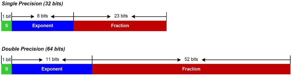
24 IEEE 754 Lecture #22 24
25 Summary Memory Read and Write Timing Expanding Memory Beyond Address Space Limits of Processor Some review of numbers today Final Lecture Review: Focused on I/O Bring Examples we can look at and work on Lecture #28 25
EE251: Thursday November 30
 EE251: Thursday November 30 Course Evaluation Forms-fill out Memory Subsystem continued Timing requirements Adding memory beyond 4 Gbyte Time Allowing: Begin Review for Final Exam Homework due next Tuesday,
EE251: Thursday November 15
 EE251: Thursday November 15 Major new topic: MEMORY A KEY topic HW #7 due today; HW #8 due Thursday, Nov. 29 Lab #8 finishes this week; due week of Nov. 26 All labs MUST be completed/handed-in by Dec.
ECE251: Thursday November 8
 ECE251: Thursday November 8 Universal Asynchronous Receiver & Transmitter Text Chapter 22, Sections 22.1.1-22.1.4-read carefully TM4C Data Sheet Section 14-no need to read this A key topic but not a lab
Ali Karimpour Associate Professor Ferdowsi University of Mashhad
 AUTOMATIC CONTROL SYSTEMS Ali Karimpour Associate Professor Ferdowsi University of Mashhad Main reference: Christopher T. Kilian, (2001), Modern Control Technology: Components and Systems Publisher: Delmar
Ali Karimpour Associate Professor Ferdowsi University of Mashhad
 AUTOMATIC CONTROL SYSTEMS Ali Karimpour Associate Professor Ferdowsi University of Mashhad Main reference: Christopher T. Kilian, (2001), Modern Control Technology: Components and Systems Publisher: Delmar
EE251: Thursday September 20
 EE251: Thursday September 20 Parallel I/O aka General Purpose I/O aka GPIO Common Devices: Switches, LEDs, Keypads Read Lab 4 carefully, and Chapter 14 in text Think about what you would like to review
CPE/EE 421/521 Fall 2004 Chapter 4 The CPU Hardware Model. Dr. Rhonda Kay Gaede UAH. The CPU Hardware Model - Overview
 CPE/EE 421/521 Fall 2004 Chapter 4 The 68000 CPU Hardware Model Dr. Rhonda Kay Gaede UAH Fall 2004 1 The 68000 CPU Hardware Model - Overview 68000 interface Timing diagram Minimal configuration using the
EE4390 Microprocessors. Lessons 2, 3 68HC12 Hardware Overview, Subsystems, and memory System
 EE4390 Microprocessors Lessons 2, 3 68HC12 Hardware Overview, Subsystems, and memory System 1 Overview 68HC12 hardware overview Subsystems Memory System 2 68HC12 Hardware Overview "Copyright of Motorola,
Understanding the basic building blocks of a microcontroller device in general. Knows the terminologies like embedded and external memory devices,
 Understanding the basic building blocks of a microcontroller device in general. Knows the terminologies like embedded and external memory devices, CISC and RISC processors etc. Knows the architecture and
Memory Expansion. Lecture Embedded Systems
 Memory Expansion Lecture 22 22-1 In These Notes... Memory Types Memory Expansion Interfacing Parallel Serial Direct Memory Access controllers 22-2 Memory Characteristics and Issues Volatility - Does it
ECE251: Thursday September 27
 ECE251: Thursday September 27 Exceptions: Interrupts and Resets Chapter in text and Lab #6. READ ALL this material! This will NOT be on the mid-term exam. Lab Practical Exam #1 Homework # due today at
1-megabit (64K x 16) 5-volt Only Flash Memory AT49F1024A Features Description Pin Configurations
 5-volt Only Flash Memory AT49F1024A Features Description Pin Configurations") BDTIC www.bdtic.com/atmel Features Single-voltage Operation 5V Read 5V Reprogramming Fast Read Access Time 45 ns Internal Program Control and Timer 8K Word Boot Block with Lockout Fast Erase Cycle Time
BDTIC www.bdtic.com/atmel Features Single-voltage Operation 5V Read 5V Reprogramming Fast Read Access Time 45 ns Internal Program Control and Timer 8K Word Boot Block with Lockout Fast Erase Cycle Time
1a)[2] Connect the devices on the left column to items on the right column. Keypad 4x4
![1a)[2] Connect the devices on the left column to items on the right column. Keypad 4x4](/thumbs/95/123675823.jpg "1a)[2] Connect the devices on the left column to items on the right column. Keypad 4x4") 2 nd Midterm ECE372 Fall 2005 This exam is: Closed book, lecture notes, calculator and internet Materials needed are in the appendix Exam duration is 75 minutes. Question Number) [Weight] I suggest that
2 nd Midterm ECE372 Fall 2005 This exam is: Closed book, lecture notes, calculator and internet Materials needed are in the appendix Exam duration is 75 minutes. Question Number) [Weight] I suggest that
Review for Exam III. Analog/Digital Converters. The MC9S12 has two 10-bit successive approximation A/D converters - can be used in 8-bit mode
 Methods used for A/D converters Flash (Parallel) Successive Approximation Review for Exam III Analog/Digital Converters A/D converters are classified according to: Resolution (number of bits) Speed (number
4-Megabit (512K x 8) 5-volt Only CMOS Flash Memory AT49F040 AT49F040T AT49F040/040T AT49F040/040T. Features. Description. Pin Configurations
 5-volt Only CMOS Flash Memory AT49F040 AT49F040T AT49F040/040T AT49F040/040T. Features. Description. Pin Configurations") Features Single Voltage Operation 5V Read 5V Reprogramming Fast Read Access Time - 70 ns Internal Program Control and Timer 16K bytes Boot Block With Lockout Fast Erase Cycle Time - 10 seconds Byte By
Features Single Voltage Operation 5V Read 5V Reprogramming Fast Read Access Time - 70 ns Internal Program Control and Timer 16K bytes Boot Block With Lockout Fast Erase Cycle Time - 10 seconds Byte By
Summer 2003 Lecture 21 07/15/03
 Summer 2003 Lecture 21 07/15/03 Simple I/O Devices Simple i/o hardware generally refers to simple input or output ports. These devices generally accept external logic signals as input and allow the CPU
Registers Format. 4.1 I/O Port Address
 4 Registers Format The detailed descriptions of the register format and structure of the ACL- 8112 are specified in this chapter. This information is quite useful for the programmer who wish to handle
May the Schwartz be with you!
 Department of Electrical & Computer Engineering Tuesday 27 June 17 29-Sep-17 3:54 PM Page 1/13 Exam 1 Instructions: Turn off cell phones beepers and other noise making devices. Show all work on the front
AT49BV004(T) TSOP Top View Type 1 1. AT49BV4096A(T) TSOP Top View Type 1 A16 BYTE GND I/O7 I/O14 I/O6 I/O13 I/O5 I/O12 I/O4 VCC I/O11 I/O3 I/O10 I/O2
 TSOP Top View Type 1 1. AT49BV4096A(T) TSOP Top View Type 1 A16 BYTE GND I/O7 I/O14 I/O6 I/O13 I/O5 I/O12 I/O4 VCC I/O11 I/O3 I/O10 I/O2") Features 2.7V to 3.6V Read/Write Operation Fast Read Access Time - 120 ns Internal Erase/Program Control Sector Architecture One 8K Words (16K bytes) Boot Block with Programming Lockout Two 4K Words (8K
Features 2.7V to 3.6V Read/Write Operation Fast Read Access Time - 120 ns Internal Erase/Program Control Sector Architecture One 8K Words (16K bytes) Boot Block with Programming Lockout Two 4K Words (8K
Select the single most appropriate response for each question. Note that none of the above MAY be a VALID ANSWER.
 ECE 362 Midterm Lab Practical - 1 - Practice Exam / Solution PART 1: Multiple Choice Select the single most appropriate response for each question. Note that none of the above MAY be a VALID ANSWER. (Solution
Topics. Interfacing chips
 8086 Interfacing ICs 2 Topics Interfacing chips Programmable Communication Interface PCI (8251) Programmable Interval Timer (8253) Programmable Peripheral Interfacing - PPI (8255) Programmable DMA controller
Interface DAC to a PC. Control Word of MC1480 DAC (or DAC 808) 8255 Design Example. Engineering 4862 Microprocessors
 8255 Design Example. Engineering 4862 Microprocessors") Interface DAC to a PC Engineering 4862 Microprocessors Lecture 22 Cheng Li EN-4012 licheng@engr.mun.ca DAC (Digital-to-Analog Converter) Device used to convert digital pulses to analog signals Two methods
Interface DAC to a PC Engineering 4862 Microprocessors Lecture 22 Cheng Li EN-4012 licheng@engr.mun.ca DAC (Digital-to-Analog Converter) Device used to convert digital pulses to analog signals Two methods
UNIT V MICRO CONTROLLER PROGRAMMING & APPLICATIONS TWO MARKS. 3.Give any two differences between microprocessor and micro controller.
 UNIT V -8051 MICRO CONTROLLER PROGRAMMING & APPLICATIONS TWO MARKS 1. What is micro controller? Micro controller is a microprocessor with limited number of RAM, ROM, I/O ports and timer on a single chip
Embedded Applications. COMP595EA Lecture03 Hardware Architecture
 Embedded Applications COMP595EA Lecture03 Hardware Architecture Microcontroller vs Microprocessor Microprocessor is a term used to describe all programmed computational devices. Microcontroller is a term
University of Florida EEL 4744 Fall 1998 Dr. Eric M. Schwartz
 Department of Electrical & Computer Engineering 15 October 199 Professor in ECE 31-Dec-9 12:22 PM Page 1/ Instructions: Show all work on the front of the test papers. If you need more room, make a clearly
ECE2049-E18 Lecture 6 Notes 1. ECE2049: Embedded Computing in Engineering Design E Term Lecture #6: Exam Review
 ECE2049-E18 Lecture 6 Notes 1 ECE2049: Embedded Computing in Engineering Design E Term 2018 Lecture #6: Exam Review Administrivia Exam 1: Next Tuesday (6/5) HW4: Short assignment, due Tuesday Lab 1: Due
ECE2049-E17 Lecture 6 1. ECE2049: Embedded Computing in Engineering Design E Term Lecture #6: Exam Review
 ECE2049-E17 Lecture 6 1 ECE2049: Embedded Computing in Engineering Design E Term 2017 Lecture #6: Exam Review Administrivia Exam 1: Next Tuesday (6/6) HW2: Due Tonight at 7pm Lab 1: Due next Tuesday (6/6),
Allmost all systems contain two main types of memory :
 Memory Interface Allmost all systems contain two main types of memory : read-only memory (ROM) system software and permanent system data random access memory (RAM) or read/write memory application software
CPE/EE 421 Microcomputers
 CPE/EE 421 Microcomputers THE 68000 CPU HARDWARE MODEL Instructor: Dr Aleksandar Milenkovic Lecture Notes Lecture 19 CPE/EE 421/521 Microcomputers 1 THE 68000 CPU HARDWARE MODEL Chapter 4 68000 interface
These three counters can be programmed for either binary or BCD count.
 S5 KTU 1 PROGRAMMABLE TIMER 8254/8253 The Intel 8253 and 8254 are Programmable Interval Timers (PTIs) designed for microprocessors to perform timing and counting functions using three 16-bit registers.
Lecture notes Lectures 1 through 5 (up through lecture 5 slide 63) Book Chapters 1-4
 Book Chapters 1-4") EE445M Midterm Study Guide (Spring 2017) (updated February 25, 2017): Instructions: Open book and open notes. No calculators or any electronic devices (turn cell phones off). Please be sure that your answers
EE445M Midterm Study Guide (Spring 2017) (updated February 25, 2017): Instructions: Open book and open notes. No calculators or any electronic devices (turn cell phones off). Please be sure that your answers
ECE 571 Advanced Microprocessor-Based Design Lecture 3
 ECE 571 Advanced Microprocessor-Based Design Lecture 3 Vince Weaver http://web.eece.maine.edu/~vweaver vincent.weaver@maine.edu 30 January 2018 Homework #1 was posted Announcements 1 Microprocessors Also
Internal architecture of 8086
 Case Study: Intel Processors Internal architecture of 8086 Slide 1 Case Study: Intel Processors FEATURES OF 8086 It is a 16-bit μp. 8086 has a 20 bit address bus can access up to 220 memory locations (1
Roberto Muscedere Images and Text Portions 2003 Prentice Hall 1
 Microcomputer Structure and Operation Chapter 5 A Microprocessor ( P) contains the controller, ALU and internal registers A Microcomputer ( C) contains a microprocessor, memory (RAM, ROM, etc), input and
ECE2049: Embedded Computing in Engineering Design A Term Fall Lecture #9: Exam Review w/ Solutions
 ECE2049: Embedded Computing in Engineering Design A Term Fall 2018 Lecture #9: Exam Review w/ Solutions Reading for Today: Review all reading and notes, Davies Ch 1, 2, 4,7, MSP430 User's Guide Ch 6.1,
Midterm Exam Review. CS 2420 :: Fall 2016 Molly O'Neil
 Midterm Exam Review CS 2420 :: Fall 2016 Molly O'Neil Midterm Exam Thursday, October 20 In class, pencil & paper exam Closed book, closed notes, no cell phones or calculators, clean desk 20% of your final
FlashFlex MCU SST89E54RD2A/RDA / SST89E58RD2A/RDA
 Introduction This document provides instructions to help programming vendors qualify the SST FlashFlex microcontrollers. Functional Blocks 8051 CPU Core ALU, ACC, B-Register, Instruction Register, Program
Microcomputer Architecture and Programming
 IUST-EE (Chapter 1) Microcomputer Architecture and Programming 1 Outline Basic Blocks of Microcomputer Typical Microcomputer Architecture The Single-Chip Microprocessor Microprocessor vs. Microcontroller
Introduction to Embedded Systems
 Stefan Kowalewski, 4. November 25 Introduction to Embedded Systems Part 2: Microcontrollers. Basics 2. Structure/elements 3. Digital I/O 4. Interrupts 5. Timers/Counters Introduction to Embedded Systems
ECSE-2610 Computer Components & Operations (COCO)
") ECSE-2610 Computer Components & Operations (COCO) Part 18: Random Access Memory 1 Read-Only Memories 2 Why ROM? Program storage Boot ROM for personal computers Complete application storage for embedded
ECSE-2610 Computer Components & Operations (COCO) Part 18: Random Access Memory 1 Read-Only Memories 2 Why ROM? Program storage Boot ROM for personal computers Complete application storage for embedded
Lecture-55 System Interface:
 Lecture-55 System Interface: To interface 8253 with 8085A processor, CS signal is to be generated. Whenever CS =0, chip is selected and depending upon A 1 and A 0 one of the internal registers is selected
The functional block diagram of 8085A is shown in fig.4.1.
 Lecture-13 Internal Architecture of Intel 05A The functional block diagram of 05A is shown in fig.4.1. INTA INTR RST7.5 RST5.5 RST6.5 TRAP SOD SID INTERRUPT SERIAL I/O (Internal Bus) FR(S) IR() B() C()
Control Unit: The control unit provides the necessary timing and control Microprocessor resembles a CPU exactly.
 Unit I 8085 and 8086 PROCESSOR Introduction to microprocessor A microprocessor is a clock-driven semiconductor device consisting of electronic logic circuits manufactured by using either a large-scale
Module 2. Embedded Processors and Memory. Version 2 EE IIT, Kharagpur 1
 Module 2 Embedded Processors and Memory Version 2 EE IIT, Kharagpur 1 Lesson 11 Embedded Processors - II Version 2 EE IIT, Kharagpur 2 Signals of a Typical Microcontroller In this lesson the student will
END-TERM EXAMINATION
 (Please Write your Exam Roll No. immediately) END-TERM EXAMINATION DECEMBER 2006 Exam. Roll No... Exam Series code: 100919DEC06200963 Paper Code: MCA-103 Subject: Digital Electronics Time: 3 Hours Maximum
PIN DIAGRAM. Richa Upadhyay Prabhu. NMIMS s MPSTME January 19, 2016
 PIN DIAGRAM Richa Upadhyay Prabhu NMIMS s MPSTME richa.upadhyay@nmims.edu January 19, 2016 Richa Upadhyay Prabhu (MPSTME) 8080 Microprocessor January 19, 2016 1 / 51 Pin Diagram of 8086 Richa Upadhyay
FlashFlex MCU SST89C58RC
 Introduction This document provides the instructions to help programming vendors qualify SST FlashFlex microcontrollers. Functional Blocks 051 CPU Core ALU, ACC, B-Register, Instruction Register, Program
CS 152 Computer Architecture and Engineering Lecture 1 Single Cycle Design
 CS 152 Computer Architecture and Engineering Lecture 1 Single Cycle Design 2014-1-21 John Lazzaro (not a prof - John is always OK) TA: Eric Love www-inst.eecs.berkeley.edu/~cs152/ Play: 1 Today s lecture
2. List the five interrupt pins available in INTR, TRAP, RST 7.5, RST 6.5, RST 5.5.
 DHANALAKSHMI COLLEGE OF ENGINEERING DEPARTMENT OF ELECTRICAL AND ELECTRONICS ENGINEERING EE6502- MICROPROCESSORS AND MICROCONTROLLERS UNIT I: 8085 PROCESSOR PART A 1. What is the need for ALE signal in
ECE2049 E17 Lecture 4 MSP430 Architecture & Intro to Digital I/O
 ECE2049-E17 Lecture 4 1 ECE2049 E17 Lecture 4 MSP430 Architecture & Intro to Digital I/O Administrivia Homework 1: Due today by 7pm o Either place in box in ECE office or give to me o Office hours tonight!
By the end of Class. Outline. Homework 5. C8051F020 Block Diagram (pg 18) Pseudo-code for Lab 1-2 due as part of prelab
 Pseudo-code for Lab 1-2 due as part of prelab") By the end of Class Pseudo-code for Lab 1-2 due as part of prelab Homework #5 on website due before next class Outline Introduce Lab 1-2 Counting Timers on C8051 Interrupts Laboratory Worksheet #05 Copy
By the end of Class Pseudo-code for Lab 1-2 due as part of prelab Homework #5 on website due before next class Outline Introduce Lab 1-2 Counting Timers on C8051 Interrupts Laboratory Worksheet #05 Copy
Infineon C167CR microcontroller, 256 kb external. RAM and 256 kb external (Flash) EEPROM. - Small single-board computer (SBC) with an
 EEPROM. - Small single-board computer (SBC) with an") Microcontroller Basics MP2-1 week lecture topics 2 Microcontroller basics - Clock generation, PLL - Address space, addressing modes - Central Processing Unit (CPU) - General Purpose Input/Output (GPIO)
Microcontroller Basics MP2-1 week lecture topics 2 Microcontroller basics - Clock generation, PLL - Address space, addressing modes - Central Processing Unit (CPU) - General Purpose Input/Output (GPIO)
Wed. Aug 23 Announcements
 Wed. Aug 23 Announcements Professor Office Hours 1:30 to 2:30 Wed/Fri EE 326A You should all be signed up for piazza Most labs done individually (if not called out in the doc) Make sure to register your
I 3 I 2. ! Language of logic design " Logic optimization, state, timing, CAD tools
 Course Wrap-up Let s Try the Priority Encoder One More Time = =! Priority Encoder Revisited! What (We Hope) You Learned I 3 O 3 I j O j! Design Methodology! I 2 O 2 I O I O Zero Oj Ij Ij CS 5 - Spring
EECS 373 Midterm 2 Fall 2018
 EECS 373 Midterm 2 Fall 2018 Name: unique name: Sign the honor code: I have neither given nor received aid on this exam nor observed anyone else doing so. Nor did I discuss this exam with anyone after
CMSC 313 COMPUTER ORGANIZATION & ASSEMBLY LANGUAGE PROGRAMMING LECTURE 09, SPRING 2013
 CMSC 313 COMPUTER ORGANIZATION & ASSEMBLY LANGUAGE PROGRAMMING LECTURE 09, SPRING 2013 TOPICS TODAY I/O Architectures Interrupts Exceptions FETCH EXECUTE CYCLE 1.7 The von Neumann Model This is a general
Computer Memory Basic Concepts. Lecture for CPSC 5155 Edward Bosworth, Ph.D. Computer Science Department Columbus State University
 Computer Memory Basic Concepts Lecture for CPSC 5155 Edward Bosworth, Ph.D. Computer Science Department Columbus State University The Memory Component The memory stores the instructions and data for an
Microprocessors/Microcontrollers
 Microprocessors/Microcontrollers A central processing unit (CPU) fabricated on one or more chips, containing the basic arithmetic, logic, and control elements of a computer that are required for processing
Address connections Data connections Selection connections
 Interface (cont..) We have four common types of memory: Read only memory ( ROM ) Flash memory ( EEPROM ) Static Random access memory ( SARAM ) Dynamic Random access memory ( DRAM ). Pin connections common
The University of Texas at Arlington Lecture 21_Review
 The University of Texas at Arlington Lecture 21_Review CSE 5442/3442 Agenda Tuesday December 1st Hand back Homework 7,8 and 9. Go over questions and answers Exam 3 Review Note: There will be a take home
1 MALP ( ) Unit-1. (1) Draw and explain the internal architecture of 8085.
 Unit-1. (1) Draw and explain the internal architecture of 8085.") (1) Draw and explain the internal architecture of 8085. The architecture of 8085 Microprocessor is shown in figure given below. The internal architecture of 8085 includes following section ALU-Arithmetic
(1) Draw and explain the internal architecture of 8085. The architecture of 8085 Microprocessor is shown in figure given below. The internal architecture of 8085 includes following section ALU-Arithmetic
University of Florida EEL 4744 Spring 2014 Dr. Eric M. Schwartz Department of Electrical & Computer Engineering 1 April Apr-14 9:03 AM
 Page 1/15 Exam 2 Instructions: Turn off cell phones beepers and other noise making devices. BEAT UCONN! Show all work on the front of the test papers. If you need more room make a clearly indicated note
ECE 2020B Fundamentals of Digital Design Spring problems, 6 pages Exam Two 26 February 2014
 Instructions: This is a closed book, closed note exam. Calculators are not permitted. If you have a question, raise your hand and I will come to you. Please work the exam in pencil and do not separate
ADM-96S AND ADM-48D HIGH PERFORMANCE DATA ACQUISITION SYSTEMS
 ADM-96S AND ADM-48D HIGH PERFORMANCE DATA ACQUISITION SYSTEMS ADM-96S DATA ACQUISITION SYSTEM 500-1-0-4100 REV.A ADM-96S / 48D VME MODULE KEY FEATURES Up to 96 Single Ended Input (ADM-96S) Up to 48 Differential
 Chapter 1 Microprocessor architecture ECE 3120 Dr. Mohamed Mahmoud http://iweb.tntech.edu/mmahmoud/ mmahmoud@tntech.edu Outline 1.1 Computer hardware organization 1.1.1 Number System 1.1.2 Computer hardware
Alex Milenkovich 1. CPE/EE 421 Microcomputers: Motorola The CPU Hardware Model. Outline
 Outline CPE/EE 421 Microcomputers: Motorola 68000 The CPU Hardware Model Instructor: Dr Aleksandar Milenkovic Lecture Notes 68000 interface Timing diagram Minimal configuration using the 68000 Extensions
A+3 A+2 A+1 A. The data bus 16-bit mode is shown in the figure below: msb. Figure bit wide data on 16-bit mode data bus
 3 BUS INTERFACE The ETRAX 100 bus interface has a 32/16-bit data bus, a 25-bit address bus, and six internally decoded chip select outputs. Six additional chip select outputs are multiplexed with other
EE 308 Spring Lecture 28 March 30, 2012 Review for Exam 2. Introduction to the MC9S12 Expanded Mode
 Lecture 28 March 30, 2012 Review for Exam 2 Introduction to the MC9S12 Expanded Mode 1 Review for Exam 2 1. C Programming (a) Setting and clearing bits in registers PORTA = PORTA 0x02; PORTA = PORTA &
Chapter 2: Fundamentals of a microprocessor based system
 Chapter 2: Fundamentals of a microprocessor based system Objectives Learn about the basic structure of microprocessor systems Learn about the memory read/write timing diagrams. Learn about address decoding
8086 INTERNAL ARCHITECTURE
 8086 INTERNAL ARCHITECTURE Segment 2 Intel 8086 Microprocessor The 8086 CPU is divided into two independent functional parts: a) The Bus interface unit (BIU) b) Execution Unit (EU) Dividing the work between
Introduction read-only memory random access memory
 Memory Interface Introduction Simple or complex, every microprocessorbased system has a memory system. Almost all systems contain two main types of memory: read-only memory (ROM) and random access memory
Am29LV081B. 8 Megabit (1 M x 8-Bit) CMOS 3.0 Volt-only Uniform Sector Flash Memory DISTINCTIVE CHARACTERISTICS
 CMOS 3.0 Volt-only Uniform Sector Flash Memory DISTINCTIVE CHARACTERISTICS") Am29LV081B 8 Megabit (1 M x 8-Bit) CMOS 3.0 Volt-only Uniform Sector Flash Memory DISTINCTIVE CHARACTERISTICS Single power supply operation 2.7 to 3.6 volt read and write operations for battery-powered
Am29LV081B 8 Megabit (1 M x 8-Bit) CMOS 3.0 Volt-only Uniform Sector Flash Memory DISTINCTIVE CHARACTERISTICS Single power supply operation 2.7 to 3.6 volt read and write operations for battery-powered
Question Bank Microprocessor and Microcontroller
 QUESTION BANK - 2 PART A 1. What is cycle stealing? (K1-CO3) During any given bus cycle, one of the system components connected to the system bus is given control of the bus. This component is said to
CprE 288 Introduction to Embedded Systems (Timers/Input Capture) Instructors: Dr. Phillip Jones
 Instructors: Dr. Phillip Jones") CprE 288 Introduction to Embedded Systems (Timers/Input Capture) Instructors: Dr. Phillip Jones 1 Announcements HW 4, Due Wed 6/13 Quiz 5 (15 min): Wed 6/13, Textbook reading: Section 9.1, 9.2 (your one-side
CprE 288 Introduction to Embedded Systems (Timers/Input Capture) Instructors: Dr. Phillip Jones 1 Announcements HW 4, Due Wed 6/13 Quiz 5 (15 min): Wed 6/13, Textbook reading: Section 9.1, 9.2 (your one-side
10/24/2016. Let s Name Some Groups of Bits. ECE 120: Introduction to Computing. We Just Need a Few More. You Want to Use What as Names?!
 University of Illinois at Urbana-Champaign Dept. of Electrical and Computer Engineering ECE 120: Introduction to Computing Memory Let s Name Some Groups of Bits I need your help. The computer we re going
INTRODUCTION TO MICROPROCESSORS
 INTRODUCTION TO MICROPROCESSORS Richa Upadhyay Prabhu NMIMS s MPSTME richa.upadhyay@nmims.edu January 7, 2016 Richa Upadhyay Prabhu (MPSTME) INTRODUCTION January 7, 2016 1 / 63 Course Design Prerequisite:
Parallel-to-Serial and Serial-to-Parallel Converters
 Session 1532 Parallel-to-Serial and Serial-to-Parallel Converters Max Rabiee, Ph.D., P.E. University of Cincinnati Abstract: Microprocessors (MPUs) on a computer motherboard communicate in a parallel format
CHETTINAD COLLEGE OF ENGINEERING AND TECHNOLOGY COMPUTER ARCHITECURE- III YEAR EEE-6 TH SEMESTER 16 MARKS QUESTION BANK UNIT-1
 CHETTINAD COLLEGE OF ENGINEERING AND TECHNOLOGY COMPUTER ARCHITECURE- III YEAR EEE-6 TH SEMESTER 16 MARKS QUESTION BANK UNIT-1 Data representation: (CHAPTER-3) 1. Discuss in brief about Data types, (8marks)
An SPI interface for the 65(C)02 family of microprocessors
02 family of microprocessors") Rev 4/B Dec 30, 2011 65SPI/B An SPI interface for the 65(C)02 family of microprocessors This device was created to provide a basic SPI interface for the 65xx family of microprocessors. Currently, the only
Rev 4/B Dec 30, 2011 65SPI/B An SPI interface for the 65(C)02 family of microprocessors This device was created to provide a basic SPI interface for the 65xx family of microprocessors. Currently, the only
M68HC08 Microcontroller The MC68HC908GP32. General Description. MCU Block Diagram CPU08 1
 M68HC08 Microcontroller The MC68HC908GP32 Babak Kia Adjunct Professor Boston University College of Engineering Email: bkia -at- bu.edu ENG SC757 - Advanced Microprocessor Design General Description The
1. INTRODUCTION TO MICROPROCESSOR AND MICROCOMPUTER ARCHITECTURE:
 1. INTRODUCTION TO MICROPROCESSOR AND MICROCOMPUTER ARCHITECTURE: A microprocessor is a programmable electronics chip that has computing and decision making capabilities similar to central processing unit
CHAPTER 1 MICROCOMPUTER SYSTEMS. 1.1 Introduction. 1.2 Microcontroller Evolution
 CHAPTER 1 MICROCOMPUTER SYSTEMS 1.1 Introduction The term microcomputer is used to describe a system that includes a microprocessor, program memory, data memory, and an input/output (I/O). Some microcomputer
CHAPTER TWELVE - Memory Devices
 CHAPTER TWELVE - Memory Devices 12.1 6x1,024 = 16,384 words; 32 bits/word; 16,384x32 = 524,288 cells 12.2 16,384 addresses; one per word. 12.3 2 16 = 65,536 words = 64K. Thus, memory capacity is 64Kx4.
538 Lecture Notes Week 5
 538 Lecture Notes Week 5 (October 4, 2017) 1/18 538 Lecture Notes Week 5 Announements Midterm: Tuesday, October 25 Answers to last week's questions 1. With the diagram shown for a port (single bit), what
ECE 331: N0. Professor Andrew Mason Michigan State University. Opening Remarks
 ECE 331: N0 ECE230 Review Professor Andrew Mason Michigan State University Spring 2013 1.1 Announcements Opening Remarks HW1 due next Mon Labs begin in week 4 No class next-next Mon MLK Day ECE230 Review
 EASWARI ENGINEERING COLLEGE DEPARTMENT OF ELECTRONICS AND COMMUNICATION QUESTION BANK - V SEMESTER ECE EC2304 MICROPROCESSORS AND MICROCONTROLLERS UNIT I 1. When the 8086 processor is in minimum mode and
1-Megabit (128K x 8) 5-volt Only Flash Memory AT29C010A. Features. Description. Pin Configurations
 5-volt Only Flash Memory AT29C010A. Features. Description. Pin Configurations") Features Fast Read Access Time - 70 ns 5-Volt Only Reprogramming Sector Program Operation Single Cycle Reprogram (Erase and Program) 1024 Sectors (128 bytes/sector) Internal Address and Data Latches for
Features Fast Read Access Time - 70 ns 5-Volt Only Reprogramming Sector Program Operation Single Cycle Reprogram (Erase and Program) 1024 Sectors (128 bytes/sector) Internal Address and Data Latches for
Microcomputers. Outline. Number Systems and Digital Logic Review
 Microcomputers Number Systems and Digital Logic Review Lecture 1-1 Outline Number systems and formats Common number systems Base Conversion Integer representation Signed integer representation Binary coded
The Memory Component
 The Computer Memory Chapter 6 forms the first of a two chapter sequence on computer memory. Topics for this chapter include. 1. A functional description of primary computer memory, sometimes called by
Intel 8086 MICROPROCESSOR. By Y V S Murthy
 Intel 8086 MICROPROCESSOR By Y V S Murthy 1 Features It is a 16-bit μp. 8086 has a 20 bit address bus can access up to 2 20 memory locations (1 MB). It can support up to 64K I/O ports. It provides 14,
Timers and Pulse Accumulator
 7 7.1 Objectives: Tiva is equipped with six General Purpose Timer Modules named TIMERn. Additionally, each TIMERn consists of two 16 bit timers (A and B). Most GPIO pins can be assigned a TIMERn as an
SRI VIDYA COLLEGE OF ENGINEERING AND TECHNOLOGY,VIRUDHUNAGAR
 Year/sem: 02/04 Academic Year: 2014-2015 (even) UNIT II THE 8086 SYSTEM BUS STRUCTURE PART A 1. What are the three groups of signals in 8086? The 8086 signals are categorized in three groups. They are:
b. List different system buses of 8085 microprocessor and give function of each bus. (8) Answer:
 Answer:") Q.2 a. Discuss and differentiate between a Microprocessor and a Microcontroller. Microprocessor is an IC which has only the CPU inside them i.e. only the processing powers such as Intel s Pentium 1,2,3,4,
Q.2 a. Discuss and differentiate between a Microprocessor and a Microcontroller. Microprocessor is an IC which has only the CPU inside them i.e. only the processing powers such as Intel s Pentium 1,2,3,4,
Embedded Systems. 3. Hardware Software Interface. Lothar Thiele. Computer Engineering and Networks Laboratory
 Embedded Systems 3. Hardware Software Interface Lothar Thiele Computer Engineering and Networks Laboratory Do you Remember? 3 2 3 3 High Level Physical View 3 4 High Level Physical View 3 5 What you will
Computer Architecture: Part III. First Semester 2013 Department of Computer Science Faculty of Science Chiang Mai University
 Computer Architecture: Part III First Semester 2013 Department of Computer Science Faculty of Science Chiang Mai University Outline Decoders Multiplexers Registers Shift Registers Binary Counters Memory
BUILDING BLOCKS OF A BASIC MICROPROCESSOR. Part 1 PowerPoint Format of Lecture 3 of Book
 BUILDING BLOCKS OF A BASIC MICROPROCESSOR Part PowerPoint Format of Lecture 3 of Book Decoder Tri-state device Full adder, full subtractor Arithmetic Logic Unit (ALU) Memories Example showing how to write
Introduction to Microcontrollers
 Introduction to Microcontrollers Embedded Controller Simply an embedded controller is a controller that is embedded in a greater system. One can define an embedded controller as a controller (or computer)
PCI to SH-3 AN Hitachi SH3 to PCI bus
 PCI to SH-3 AN Hitachi SH3 to PCI bus Version 1.0 Application Note FEATURES GENERAL DESCRIPTION Complete Application Note for designing a PCI adapter or embedded system based on the Hitachi SH-3 including:
2. (2 pts) If an external clock is used, which pin of the 8051 should it be connected to?
 If an external clock is used, which pin of the 8051 should it be connected to?") ECE3710 Exam 2. Name _ Spring 2013. 5 pages. 102 points, but scored out of 100. You may use any non-living resource to complete this exam. Any hint of cheating will result in a 0. Part 1 Short Answer 1.
ECE3710 Exam 2. Name _ Spring 2013. 5 pages. 102 points, but scored out of 100. You may use any non-living resource to complete this exam. Any hint of cheating will result in a 0. Part 1 Short Answer 1.
EC 6504 Microprocessor and Microcontroller. Unit II System Bus Structure
 EC 6504 Microprocessor and Microcontroller Unit II 8086 System Bus Structure Syllabus: 8086 Signals Basic Configurations System bus timing System Design using 8086 IO Programming Introduction to multiprogramming