Tutorial for Cadence SOC Encounter Place & Route
|
|
|
- Hannah Poole
- 6 years ago
- Views:
Transcription
1 Tutorial for Cadence SOC Encounter Place & Route For Encounter RTL-to-GDSII System T. Manikas, Southern Methodist University, 3/9/15 Contents 1 Preliminary Setup Helpful Hints Starting Tool and Reading in the Design Files Saving and Restoring Your Design Floorplanning Specify Floorplan Power Planning Connect Global Nets Power Rings Power Stripes Connect Power to Standard Cell Rows Placing the Standard Cells Routing Adding Filler Cells Preliminary Setup Create a separate directory for the above files in your account (e.g., Encounter). Create the subdirectories synth and lib 1. Move full_adder_pads_syn.v to the synth directory 2. Move osu05_stdcells.lef to the lib directory 1.1 Helpful Hints 1. Some of the pop-up windows may be too big for your screen, making it hard to access the button on the bottom of the window. To move a window in X-windows, point your mouse anywhere in the window and press the ALT key and the right mouse button. 1
 as mentioned earlier 2.")

2 2 Starting Tool and Reading in the Design Files 1. Make sure that you are in your main separate directory (e.g., Encounter) as mentioned earlier 2. At the Unix prompt, type: encounter 3. When the Encounter tool window appears, go to the menu bar and select File, Import Design to get the Design Import window. 4. For the Verilog Netlist, click on the box with the dots [ ] to open the Netlist Files window 2


3 5. Click on the ">>" button to expand the window to show the directories: 3
4 6. Double-click on the synth folder, then select the file full_adder_pads_syn.v and click the Add button to add it to the Netlist Files list. Click Close to close the Netlist Files window. 4
5 7. In the main window, for Top Cell, select "Auto Assign" 5

6 8. For Technology/Physical Libraries, select "LEF Files". Click on the [ ] button open the LEF Files window. 6
7 9. Using the same approach as for selecting the Verilog Netlist file, select the file lib/osu05_stdcells.lef 7

8 10. For Power, enter the following: a. Power Nets: vdd b. Ground Nets: gnd 11. Click on OK. 8
9 2.1 Saving and Restoring Your Design NOTE: It is a good idea to save your design periodically. Select File, Save Design. In the Save Design Window, select Data Type: Encounter. The program will assign a default filename with extension *.enc. You may change the name, but do not change the extension. 9

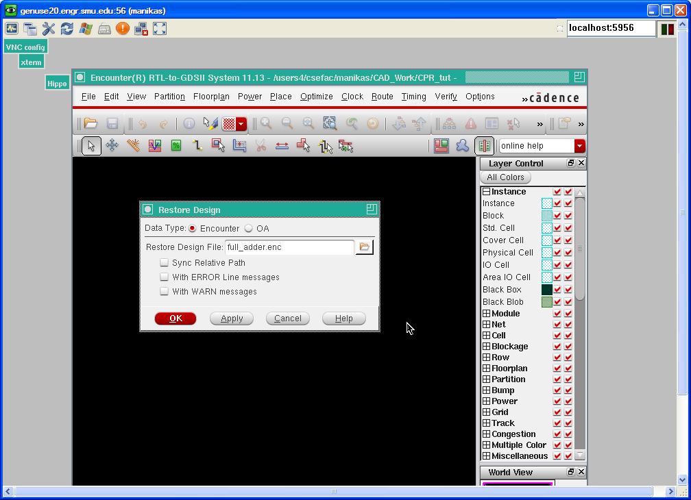
10 To load a saved Encounter file, do File, Restore Design. In the Restore Design Window, select Data Type: Encounter. Select the file to be restored. 10
11 11

12 3 Floorplanning 3.1 Specify Floorplan In Encounter tool menu bar, select Floorplan, Specify Floorplan to get the Specify Floorplan window. 1. In the Basic tab, select the following options: a. Core Margins select Core to IO Boundary and set all margins to Click on OK. 12
13 13
 in the following boxes: i. \"To Global Net\" ii.")
14 4 Power Planning 4.1 Connect Global Nets In Encounter tool menu bar, select Power, Connect Global Nets to get the Global Net Connections Window. 1. In Power Ground Connection a. In the Connect area, select Pin b. In the Scope area, select Apply All 2. For each net vdd and gnd, do the following: a. Enter the net name (vdd or gnd) in the following boxes: i. "To Global Net" ii. "Pin Name(s)" b. Click on the "Add to List" button 3. Click Apply, then click Cancel 14
, enter vdd and gnd nets as follows: a. Click on [ ] box to get Net Selection window b. Select vdd and gnd from Possible Nets column c.")
15 4.2 Power Rings In Encounter tool menu bar, select Power, Power Planning, Add Rings to get the Add Rings window. 1. For Net(s), enter vdd and gnd nets as follows: a. Click on [ ] box to get Net Selection window b. Select vdd and gnd from Possible Nets column c. Click Add to copy to Chosen Nets column d. Click OK 15

16 2. In Ring Configuration, select metal1 for Top and Bottom, metal2 for Left and Right. a. Width should be 8 b. Spacing should be 1 c. Offset should be Center in channel 3. Click OK 16
17 17

18 4.3 Power Stripes In Encounter tool menu bar, select Power, Power Planning, Add Stripes to get the Add Stripes window. 1. Basic Tab a. For Net(s), enter vdd and gnd nets as follows: i. Click on [ ] box to get Net Selection window ii. Select vdd and gnd from Possible Nets column iii. Click Add to copy to Chosen Nets column iv. Click OK b. In Set Configuration, select Layer metal2 and Direction vertical. Width should be 8 and Spacing should be 1. c. In Set Pattern, set Set-to-set distance to 100 d. In First/Last Stripe, select Relative from core or selected area, X from left to 20 18

19 2. Advanced Tab a. Set Snap wire center to routing grid as Grid 3. Click OK NOTE: MAY NEED TO USE ALT-RIGHT MOUSE TO MOVE WINDOW TO GET TO OK BUTTON (SEE HINT IN SECTION 1.1 above). 19
20 20
21 21
22 4.4 Connect Power to Standard Cell Rows In Encounter tool menu bar, select Route, Special Route, and click OK. This will create power (vdd) and ground (gnd) rails for your standard cell rows. Save your design using the procedure described in Section 2.1 above. 22


23 5 Placing the Standard Cells In Encounter tool menu bar, select Place, Standard Cells to get the Place window. 1. Select Run Full Placement and Include Pre-Place Optimization 2. Click OK After cells are placed, change to Physical View in the Encounter Window to see placement results. 23
24 24

25 6 Routing In Encounter tool menu bar, select Route, NanoRoute, Route to get the NanoRoute window. 1. Click OK. 25

26 26

27 7 Adding Filler Cells 1. Now that we have routed all the wires and placed all the cell in our design, we will add empty filler cells to the design. Select Place, Physical Cell, Add Filler. 2. In the Add Filler window, enter the Cell Name FILL and check Mark Fixed. Click OK. 27

28 3. Note that filer cells are added to the layout: 28
Tutorial 2 Automatic Placement & Routing
 Tutorial 2 Automatic Placement & Routing Please follow the instructions found under Setup on the CADTA main page before starting this tutorial. 1.1. Start Encounter Log on to a VLSI server using your EE
Laboratory 6. - Using Encounter for Automatic Place and Route. By Mulong Li, 2013
 CME 342 (VLSI Circuit Design) Laboratory 6 - Using Encounter for Automatic Place and Route By Mulong Li, 2013 Reference: Digital VLSI Chip Design with Cadence and Synopsys CAD Tools, Erik Brunvand Background
Tutorial for Encounter
 Tutorial for Encounter STEP 1: Login to the Linux system on Linuxlab server. Start a terminal (the shell prompt). (If you don t know how to login to Linuxlab server, look at here) Click here to open a
EE 330 Laboratory Experiment Number 11
 EE 330 Laboratory Experiment Number 11 Design and Simulation of Digital Circuits using Hardware Description Languages Fall 2017 Contents Purpose:... 3 Background... 3 Part 1: Inverter... 4 1.1 Simulating
Cell-Based IC Physical Design & Verification SOC Encounter. Advisor : 李昆忠 Presenter : 蕭智元
 Cell-Based IC Physical Design & Verification SOC Encounter Advisor : 李昆忠 Presenter : 蕭智元 Reference: SOC Encounter Training Manual, 2007, edited by CIC. Introduction We ll use some EDA tools to transform
Physical Placement with Cadence SoCEncounter 7.1
 Physical Placement with Cadence SoCEncounter 7.1 Joachim Rodrigues Department of Electrical and Information Technology Lund University Lund, Sweden November 2008 Address for correspondence: Joachim Rodrigues
Tutorial I: Cadence Innovus ECE6133: Physical Design Automation of VLSI Systems Georgia Institute of Technology Prof. Sung Kyu Lim
 Tutorial I: Cadence Innovus ECE6133: Physical Design Automation of VLSI Systems Georgia Institute of Technology Prof. Sung Kyu Lim I. Setup for Cadence Innovus 1. Copy the following files into your working
Cadence SOC Encounter Tutorial for a logic block using the University Of Utah Standard cell Libraries In ON Semiconductor 0.
 Cadence SOC Encounter Tutorial for a logic block using the University Of Utah Standard cell Libraries In ON Semiconductor 0.5 µ C5N CMOS 1. Create a folder called encounter inside of your project folder
EE 330 Laboratory Experiment Number 11 Design, Simulation and Layout of Digital Circuits using Hardware Description Languages
 EE 330 Laboratory Experiment Number 11 Design, Simulation and Layout of Digital Circuits using Hardware Description Languages Purpose: The purpose of this experiment is to develop methods for using Hardware
EE 330 Laboratory Experiment Number 11 Design and Simulation of Digital Circuits using Hardware Description Languages
 EE 330 Laboratory Experiment Number 11 Design and Simulation of Digital Circuits using Hardware Description Languages Fall 2015 Purpose: The purpose of this experiment is to develop methods for using Hardware
Creating Verilog Tutorial Netlist Release Date: 01/13/2005(Version 2)
") Creating Verilog Tutorial 2-1 - Creating a verilog netlist for a schematic: The verilog netlist is necessary for automatic layout (placement and routing) tools. It contains information about the I/O pins
Creating Verilog Tutorial 2-1 - Creating a verilog netlist for a schematic: The verilog netlist is necessary for automatic layout (placement and routing) tools. It contains information about the I/O pins
Outline. SoC Encounter Flow. Typical Backend Design Flow. Digital IC-Project and Verification. Place and Route. Backend ASIC Design flow
 Outline Digital IC-Project and Verification Deepak Dasalukunte Backend ASIC Design flow General steps Input files Floorplanning Placement Clock-synthesis Routing Typical Backend Design Flow SoC Encounter
ECE425: Introduction to VLSI System Design Machine Problem 3 Due: 11:59pm Friday, Dec. 15 th 2017
 ECE425: Introduction to VLSI System Design Machine Problem 3 Due: 11:59pm Friday, Dec. 15 th 2017 In this MP, you will use automated tools to synthesize the controller module from your MP2 project into
Place & Route: Using Silicon Ensemble
 Place & Route: Using Silicon Ensemble Introduction In a typical digital design flow, hardware description language is used to model a design and verify desired behavior. Once the desired functionality
CMOS VLSI Design Lab 3: Controller Design and Verification
 CMOS VLSI Design Lab 3: Controller Design and Verification The controller for your MIPS processor is responsible for generating the signals to the datapath to fetch and execute each instruction. It lacks
Synthesis and APR Tools Tutorial
 Synthesis and APR Tools Tutorial (Last updated: Oct. 26, 2008) Introduction This tutorial will get you familiarized with the design flow of synthesizing and place and routing a Verilog module. All the
CMOS VLSI Design Lab 3: Controller Design and Verification
 CMOS VLSI Design Lab 3: Controller Design and Verification The controller for your MIPS processor is responsible for generating the signals to the datapath to fetch and execute each instruction. It lacks
CMOS VLSI Design Lab 3: Controller Design and Verification
 CMOS VLSI Design Lab 3: Controller Design and Verification The controller for your MIPS processor is responsible for generating the signals to the datapath to fetch and execute each instruction. It lacks
Creating LEF File. Abstract Generation: Creating LEF Tutorial File Release Date: 01/13/2004. Export GDS:
 Creating LEF Tutorial 1-1 - Creating LEF File Abstract Generation: Export GDS: Abstract generator comes as a part of the Silicon Ensemble package. As such, it cannot directly read ICFB library databases.
Cadence On-Line Document
 Cadence On-Line Document 1 Purpose: Use Cadence On-Line Document to look up command/syntax in SoC Encounter. 2 Cadence On-Line Document An on-line searching system which can be used to inquire about LEF/DEF
Abstract Editor (Last updated: Oct. 23, 2008)
") Abstract Editor (Last updated: Oct. 23, 2008) Abstract Editor Tutorial This tutorial has been created to discuss all of the steps needed to create an abstract Library Exchange Format (LEF) file for custom
Abstract Editor (Last updated: Oct. 23, 2008) Abstract Editor Tutorial This tutorial has been created to discuss all of the steps needed to create an abstract Library Exchange Format (LEF) file for custom
Digital IC- Project 1. Place and Route. Oskar Andersson. Oskar Andersson, EIT, LTH, Digital IC project and Verifica=on
 Digital IC- Project 1 Oskar Andersson Outline Backend ASIC Design flow (Physical Design) General steps Input files Floorplanning Placement ClockTree- synthesis Rou=ng Typical Backend Design Flow Synthesis
CS 4120 Hardware Description Languages and Synthesis Homework 6: Introduction to Cadence Silicon Ensemble
 CS 4120 Hardware Description Languages and Synthesis Homework 6: Introduction to Cadence Silicon Ensemble 0. Introduction In this homework, you will be introduced to a Place and Route tool called Silicon
TUTORIAL II ECE 555 / 755 Updated on September 11 th 2006 CADENCE LAYOUT AND PARASITIC EXTRACTION
 TUTORIAL II ECE 555 / 755 Updated on September 11 th 2006 CADENCE LAYOUT AND PARASITIC EXTRACTION After finishing a schematic of your design (Tutorial-I), the next step is creating masks which are for
Another view of the standard cells called the abstract view needs to generated
 Abstract Generation Place and route tools do not require the full cell layout Another view of the standard cells called the abstract view needs to generated The abstract view provides information like:
CADENCE TUTORIAL. San Diego State University, Department of Electrical and Computer Engineering. Amith Dharwadkar and Ashkan Ashrafi
 CADENCE TUTORIAL San Diego State University, Department of Electrical and Computer Engineering Amith Dharwadkar and Ashkan Ashrafi 1 Contents 1) 2) 3) 4) 5) 6) Introduction 3 Connecting to the Volta server..4
EE115C Digital Electronic Circuits. Tutorial 4: Schematic-driven Layout (Virtuoso XL)
") EE115C Digital Electronic Circuits Tutorial 4: Schematic-driven Layout (Virtuoso XL) This tutorial will demonstrate schematic-driven layout on the example of a 2-input NAND gate. Simple Layout (that won
EE115C Digital Electronic Circuits Tutorial 4: Schematic-driven Layout (Virtuoso XL) This tutorial will demonstrate schematic-driven layout on the example of a 2-input NAND gate. Simple Layout (that won
VLSI Lab Tutorial 1. Cadence Virtuoso Schematic Composer Introduction
 VLSI Lab Tutorial 1 Cadence Virtuoso Schematic Composer Introduction 1.0 Introduction The purpose of the first lab tutorial is to help you become familiar with the schematic editor, Virtuoso Schematic
Virtuoso Layout Editor
 This tutorial will cover the basic steps involved in using the Cadence layout editor called Virtuoso, extracting layout, and running simulation on the layout. The inverter layout is used as an example
Lesson 9: Processing a Schematic Design
 Lesson 9: Processing a Schematic Design Lesson Objectives After you complete this lab you will be able to: Assign reference designators Check the design for errors Create a netlist for OrCAD and Allegro
Part B. Dengxue Yan Washington University in St. Louis
 Tools Tutorials Part B Dengxue Yan Washington University in St. Louis Tools mainly used in this class Synopsys VCS Simulation Synopsys Design Compiler Generate gate-level netlist Cadence Encounter placing
ASIC Physical Design Top-Level Chip Layout
 ASIC Physical Design Top-Level Chip Layout References: M. Smith, Application Specific Integrated Circuits, Chap. 16 Cadence Virtuoso User Manual Top-level IC design process Typically done before individual
Virtuoso Schematic Composer
 is a schematic design tool from Cadence. In this tutorial you will learn how to put electrical components, make wire connections, insert pins and check for connection error. Start Cadence Custom IC Design
EE434 ASIC & Digital Systems. From Layout to SPICE Simulation (Virtuoso, Calibre, HSpice) Spring 2017 Dae Hyun Kim
 Spring 2017 Dae Hyun Kim") EE434 ASIC & Digital Systems From Layout to SPICE Simulation (Virtuoso, Calibre, HSpice) Spring 2017 Dae Hyun Kim daehyun@eecs.wsu.edu 1 Preparation for Lab2 Download the following file into your working
EE434 ASIC & Digital Systems From Layout to SPICE Simulation (Virtuoso, Calibre, HSpice) Spring 2017 Dae Hyun Kim daehyun@eecs.wsu.edu 1 Preparation for Lab2 Download the following file into your working
ECE471/571 Energy Efficient VLSI Design Project 2 Cadence Setup and Creation of an Inverter Due Date 11:30 am on Friday, February 2 nd, 2018
 ECE471/571 Energy Efficient VLSI Design Project 2 Cadence Setup and Creation of an Inverter Due Date 11:30 am on Friday, February 2 nd, 2018 Introduction This project will first walk you through the setup
An Overview of Standard Cell Based Digital VLSI Design
 An Overview of Standard Cell Based Digital VLSI Design With examples taken from the implementation of the 36-core AsAP1 chip and the 1000-core KiloCore chip Zhiyi Yu, Tinoosh Mohsenin, Aaron Stillmaker,
Cadence Tutorial A: Schematic Entry and Functional Simulation Created for the MSU VLSI program by Andrew Mason and the AMSaC lab group.
 Cadence Tutorial A: Schematic Entry and Functional Simulation Created for the MSU VLSI program by Andrew Mason and the AMSaC lab group. Revision Notes: Aug. 2003 update and edit A. Mason add intro/revision/contents
An overview of standard cell based digital VLSI design
 An overview of standard cell based digital VLSI design Implementation of the first generation AsAP processor Zhiyi Yu and Tinoosh Mohsenin VCL Laboratory UC Davis Outline Overview of standard cellbased
Exercise 1. Section 2. Working in Capture
 Exercise 1 Section 1. Introduction In this exercise, a simple circuit will be drawn in OrCAD Capture and a netlist file will be generated. Then the netlist file will be read into OrCAD Layout. In Layout,
Introduction to Design Architect
 SANTA CLARA UNIVERSITY Dept. of Electrical Engineering Mentor Graphics Tutorials Introduction to Design Architect Yiching Chen Sangeetha Raman S. Krishnan I. Introduction II. This document contains a step-by-step
Procedure for PCBoard Layout
 Procedure for PCBoard Layout Introduction The following 6 pages of instructions will take you step by step through the creation of your PCB using Orcad Layout. If you are planning to manually lay out your
DRC and LVS checks using Cadence Virtuoso Version 3.0
 DRC and LVS checks using Cadence Virtuoso Version 3.0 Start virtuoso l l Open a virtuoso session in the directory which contains the required cds.lib and lib.def files. Command : virtuoso & Open the layout
Design rule illustrations for the AMI C5N process can be found at:
 Cadence Tutorial B: Layout, DRC, Extraction, and LVS Created for the MSU VLSI program by Professor A. Mason and the AMSaC lab group. Revised by C Young & Waqar A Qureshi -FS08 Document Contents Introduction
EECS 627, Lab Assignment 3
 EECS 627, Lab Assignment 3 1 Introduction In this lab assignment, we will use Cadence ICFB and Calibre to become familiar with the process of DRC/LVS checks on a design. So far, we have placed and routed
Simulating a Design Circuit Using Qsim
 Simulating a Design Circuit Using Qsim 1. Start Qsim From version 11.1, Quartus II provides another simulating tool called Qsim. Qsim is bundled with both subscript edition and web edition of Quartus II.
OrCad & Spice Tutorial By, Ronak Gandhi Syracuse University
 OrCad & Spice Tutorial By, Ronak Gandhi Syracuse University Brief overview: OrCad is a suite of tools from Cadence for the design and layout of circuit design and PCB design. We are currently using version
Amplifier Simulation Tutorial. Design Kit: Cadence 0.18μm CMOS PDK (gpdk180) (Cadence Version 6.1.5)
 (Cadence Version 6.1.5)") Amplifier Simulation Tutorial Design Kit: Cadence 0.18μm CMOS PDK (gpdk180) (Cadence Version 6.1.5) Yongsuk Choi, Marvin Onabajo This tutorial provides a quick introduction to the use of Cadence tools
Amplifier Simulation Tutorial Design Kit: Cadence 0.18μm CMOS PDK (gpdk180) (Cadence Version 6.1.5) Yongsuk Choi, Marvin Onabajo This tutorial provides a quick introduction to the use of Cadence tools
HOMEWORK 9 CMPEN 411 Due: 4/12/ :30pm
 HOMEWORK 9 CMPEN 411 Due: 4/12/2016 11:30pm Learning Objective Complete the full 8 bit RISC microprocessor chip design by placing the processor core design into the 40 pin 'tiny' chip pad frame. Do verify
Cadence Tutorial 2: Layout, DRC/LVS and Circuit Simulation with Extracted Parasitics
 Cadence Tutorial 2: Layout, DRC/LVS and Circuit Simulation with Extracted Parasitics Introduction This tutorial describes how to generate a mask layout in the Cadence Virtuoso Layout Editor. Use of DIVA
UNIVERSITY OF WATERLOO
 UNIVERSITY OF WATERLOO UW ASIC DESIGN TEAM: Cadence Tutorial Description: Part I: Layout & DRC of a CMOS inverter. Part II: Extraction & LVS of a CMOS inverter. Part III: Post-Layout Simulation. The Cadence
From SOC Encounter to Virtuoso (version 3.1)
") From SOC Encounter to Virtuoso (version 3.1) Alberto Stabile 20 Gen. 2011 1 Indroduction This little example has been created to check the design ow with 65-nm TSMC. The ow starts from an ad-hoc Verilog
From SOC Encounter to Virtuoso (version 3.1) Alberto Stabile 20 Gen. 2011 1 Indroduction This little example has been created to check the design ow with 65-nm TSMC. The ow starts from an ad-hoc Verilog
AMIS CDNLive Paper: A DFII Based Place and Route Interface
 Table of Contents Chapter 1.0 Overview Chapter 2.0 Implementation Chapter 3.0 Digital Integration Form Chapter 4.0 To P&R Tab Chapter 5.0 From P&R Tab Chapter 6.0 Summary 1/17 Introduction Chapter 1: Overview
The IIT standard cell library Version 2.1
 The IIT standard cell library Version 2.1 Highlights - Support for AMI 0.35um library, including pads - Added Primetime and Pathmill support to IIT ASIC Flow - Support for stacked vias (for Virtuoso and
Pipelined MIPS CPU Synthesis and On-Die Representation ECE472 Joseph Crop Stewart Myers
 Pipelined MIPS CPU Synthesis and On-Die Representation ECE472 Joseph Crop Stewart Myers 2008 Table of Contents Introduction... 3 Steps Taken and Simulation... 3 Pitfalls... 8 Simulated Delay... 9 APPENDIX
ESE 570 Cadence Lab Assignment 2: Introduction to Spectre, Manual Layout Drawing and Post Layout Simulation (PLS)
") ESE 570 Cadence Lab Assignment 2: Introduction to Spectre, Manual Layout Drawing and Post Layout Simulation (PLS) Objective Part A: To become acquainted with Spectre (or HSpice) by simulating an inverter,
ESE 570 Cadence Lab Assignment 2: Introduction to Spectre, Manual Layout Drawing and Post Layout Simulation (PLS) Objective Part A: To become acquainted with Spectre (or HSpice) by simulating an inverter,
VLSI Lab Tutorial 3. Virtuoso Layout Editing Introduction
 VLSI Lab Tutorial 3 Virtuoso Layout Editing Introduction 1.0 Introduction The purpose of this lab tutorial is to guide you through the design process in creating a custom IC layout for your CMOS inverter
Analog IC Schematic Capture. Mentor Graphics 2006
 Analog IC Schematic Capture Mentor Graphics 2006 Santa Clara University Department of Electrical Engineering Date of Last Revision: February 6, 2007 Table of Contents 1. Objective...3 2. Setup & Preparation...4
ECE471/571 Energy Ecient VLSI Design
 ECE471/571 Energy Ecient VLSI Design Project 2 Cadence Setup and Creation of an Inverter Due Date 11:30pm on Friday, January 30 th 2015 Introduction This project will rst walk you through the setup for
Tutorial 3 - Performing a Change-Point Analysis in Excel
 Tutorial 3 - Performing a Change-Point Analysis in Excel Introduction This tutorial teaches you how to perform a change-point analysis while using Microsoft Excel. The Change-Point Analyzer Add-In allows
Cadence IC Design Manual
 Cadence IC Design Manual For EE5518 ZHENG Huan Qun Lin Long Yang Revised on May 2017 Department of Electrical & Computer Engineering National University of Singapore 1 P age Contents 1 INTRODUCTION...
How to Get Started. Figure 3
 Tutorial PSpice How to Get Started To start a simulation, begin by going to the Start button on the Windows toolbar, then select Engineering Tools, then OrCAD Demo. From now on the document menu selection
Lesson 5: Board Design Files
 5 Lesson 5: Board Design Files Learning Objectives In this lesson you will: Use the Mechanical Symbol Editor to create a mechanical board symbol Use the PCB Design Editor to create a master board design
FACULTY OF ENGINEERING MULTIMEDIA UNIVERSITY LAB SHEET DIGITAL INTEGRATED CIRCUIT
 FACULTY OF ENGINEERING MULTIMEDIA UNIVERSITY LAB SHEET DIGITAL INTEGRATED CIRCUIT DIC1: Schematic Design Entry, Simulation & Verification DIC2: Schematic Driven Layout Drawing (SDL) Design Rule Check (DRC)
Select the technology library: NCSU_TechLib_ami06, then press OK.
 ECE 126 Inverter Tutorial: Schematic & Symbol Creation Created for GWU by Anis Nurashikin Nordin & Thomas Farmer Tutorial adapted from: http://www.ee.ttu.edu/ee/cadence/commondirectory/final%20tutorials/digitalcircuitsimulationusingvirtuoso.doc
Orcad Layout Plus Tutorial
 Orcad Layout Plus Tutorial Layout Plus is a circuit board layout tool that accepts a layout-compatible circuit netlist (ex. from Capture CIS) and generates an output layout files that suitable for PCB
S Exercise 1C Testing the Ring Oscillator
 S-87.3148 Exercise 1C Testing the Ring Oscillator Aalto University School of Electrical Engineering Department of Micro- and Nanosciences (ECDL) 10.9.2014 1 1 Building the test bench In this exercise,
Instruction on padframe
 Instruction on padframe The padframe is a 40-pins padframe for the AMI ABN 1.6um process from MOSIS located at http://www.mosis.org/cell-libraries/scn16-pads/. You should download the CIF file from the
Synopsys Custom Designer Tutorial for a chip integra7on using the University of Utah Standard Cell Libraries In ON Semiconductor 0.
 Synopsys Custom Designer Tutorial for a chip integra7on using the University of Utah Standard Cell Libraries In ON Semiconductor 0.5u C5 CMOS Version 6.0 Overview This tutorial will take you through the
CMOS Design Lab Manual
 CMOS Design Lab Manual Developed By University Program Team CoreEl Technologies (I) Pvt. Ltd. 1 Objective Objective of this lab is to learn the Mentor Graphics HEP2 tools as well learn the flow of the
Asic Design ET Alexander de Graaf, EEMCS/ME/CAS 5/20/14. Challenge the future. Delft University of Technology
 Asic Design ET 4351 Alexander de Graaf, EEMCS/ME/CAS 5/20/14 Delft University of Technology Challenge the future Outline. 1. Design flow 2. Synthesis 3. Place & Route ASIC Design: Backend 2 100 1. Design
C Allegro Package Designer Flows
 1 Allegro User Guide: Getting Started with Physical Design Product Version 16.6 October 2012 C Allegro Package Designer Flows This appendix presents design flows that illustrate the use of the Allegro
Prepared by Dr. Ulkuhan Guler GT-Bionics Lab Georgia Institute of Technology
 Prepared by Dr. Ulkuhan Guler GT-Bionics Lab Georgia Institute of Technology OUTLINE Introduction Mapping for Schematic and Layout Connectivity Generate Layout from Schematic Connectivity Some Useful Features
Cell-Based Design Flow. TA : 吳廸優
 Cell-Based Design Flow TA : 吳廸優 dywu@viplab.cs.nctu.edu.tw 1 Outline Overview Design Flow Stage 1 RTL Development Synthesis Gate Level Simulation Design Flow Stage 2 Placement and Routing Post Layout Simulation
UNIVERSITY OF CALIFORNIA College of Engineering Department of Electrical Engineering and Computer Sciences Lab #2: Layout and Simulation
 UNIVERSITY OF CALIFORNIA College of Engineering Department of Electrical Engineering and Computer Sciences Lab #2: Layout and Simulation NTU IC541CA 1 Assumed Knowledge This lab assumes use of the Electric
Cadence Tutorial A: Schematic Entry and Functional Simulation Created for the MSU VLSI program by Professor A. Mason and the AMSaC lab group.
 Cadence Tutorial A: Schematic Entry and Functional Simulation Created for the MSU VLSI program by Professor A. Mason and the AMSaC lab group. Revision Notes: Jan. 2006 Updated for use with spectre simulator
Tutorial II: Cadence Virtuoso ECE6133: Physical Design Automation of VLSI Systems Georgia Institute of Technology Prof.
 Tutorial II: Cadence Virtuoso ECE6133: Physical Design Automation of VLSI Systems Georgia Institute of Technology Prof. Sung Kyu Lim I. Setup for Cadence Virtuoso 1. Copy the following files into your
Lecture Content. 1 Adam Teman, 2018
 Lecture Content 1 Adam Teman, 2018 Digital VLSI Design Lecture 6: Moving to the Physical Domain Semester A, 2018-19 Lecturer: Dr. Adam Teman December 24, 2018 Disclaimer: This course was prepared, in its
HOMEWORK 10 CMPEN 411 Due: 4/28/ :30pm
 HOMEWORK 10 CMPEN 411 Due: 4/28/2016 11:30pm Instruction First, fabrication ready the full 8 bit RISC microprocessor chip: redesign the chip (its components) to fit the entire chip fitted into the 40 pin
Introduction to Innovus
 Introduction to Innovus Courtesy of Dr. Dae Hyun Kim@WSU http://csce.uark.edu +1 (479) 575-6043 yrpeng@uark.edu Introduction to Innovus Innovus was called Innovus before v15 Standard Placement and Routing
RTL Design and IP Generation Tutorial. PlanAhead Design Tool
 RTL Design and IP Generation Tutorial PlanAhead Design Tool Notice of Disclaimer The information disclosed to you hereunder (the "Materials") is provided solely for the selection and use of Xilinx products.
- create new schematic to the new project, PCB design begins with a schematic diagram, which present how components are connected
 Eagle 8.x tutorial - create a new project, Eagle designs are organized as projects - create new schematic to the new project, PCB design begins with a schematic diagram, which present how components are
Revision Notes: July2004 Generate tutorial for single transistor analysis. Based on existing schematic entry tutorial developed for ECE410
 Cadence Analog Tutorial 1: Schematic Entry and Transistor Characterization Created for the MSU VLSI program by Professor A. Mason and the AMSaC lab group. Revision Notes: July2004 Generate tutorial for
PlanAhead Software Tutorial
 PlanAhead Software Tutorial RTL Design and IP Generation The information disclosed to you hereunder (the Information ) is provided AS-IS with no warranty of any kind, express or implied. Xilinx does not
EECS 627, Lab Assignment 2
 EECS 627, Lab Assignment 2 1 Introduction In this lab assignment, you will extend the process of designing your multiplier chip. You will add two more blocks (a pseudo-random test pattern generator and
Malikarjun Avula, Emil Jovanov Electrical and Computer Engineering Department University of Alabama in Huntsville CPE 495 September 03, 2009
 Malikarjun Avula, Emil Jovanov Electrical and Computer Engineering Department University of Alabama in Huntsville CPE 495 September 03, 2009 Agenda PCB Design Process General Guidelines Express SCH Getting
Place & Route Tutorial #1
 Place & Route Tutorial #1 In this tutorial you will use Synopsys IC Compiler (ICC) to place, route, and analyze the timing and wirelength of two simple designs. This tutorial assumes that you have worked
Creating More Detailed Forms
 Creating More Detailed Forms Chapter 5 When databases become larger it is necessary to be able move fields anywhere on the screen so that all the data can be clearly displayed. Access allows you to produce
CPE/EE 427, CPE 527, VLSI Design I: Tutorial #2, Schematic Capture, DC Analysis, Transient Analysis (Inverter, NAND2)
") CPE/EE 427, CPE 527, VLSI Design I: Tutorial #2, Schematic Capture, DC Analysis, Transient Analysis (Inverter, NAND2) Joel Wilder, Aleksandar Milenkovic, ECE Dept., The University of Alabama in Huntsville
CPE/EE 427, CPE 527, VLSI Design I: Tutorial #2, Schematic Capture, DC Analysis, Transient Analysis (Inverter, NAND2) Joel Wilder, Aleksandar Milenkovic, ECE Dept., The University of Alabama in Huntsville
Creating a Multi-line Plate
 Creating a Multi-line Plate The following steps demonstrate how to create a multi-line plate, which will then be used to create a series of badges. Initial Setup Before beginning the procedure, the following
ASIC Physical Design Standard-Cell Design Flow. Using the Cadence Encounter Digital Implementation System
 ASIC Physical Design Standard-Cell Design Flow Using the Cadence Encounter Digital Implementation System ASIC Physical Design (Standard Cell) (can also do full custom layout) Component-Level Verilog Netlist
Batch Processing: The Complete Synthesize, Place, and Route Flow
 Batch Processing: The Complete Synthesize, Place, and Route Flow Daniel Liu, John Lee, Puneet Gupta University of California, Los Angeles, NanoCAD Lab {daniel,lee,puneet}@ee.ucla.edu Abstract Design automation
Eliminating Routing Congestion Issues with Logic Synthesis
 Eliminating Routing Congestion Issues with Logic Synthesis By Mike Clarke, Diego Hammerschlag, Matt Rardon, and Ankush Sood Routing congestion, which results when too many routes need to go through an
Using the ispxpga Floorplanner
 Using the ispxpga Floorplanner Table of Contents USING THE ISPXPGA FLOORPLANNER...3 Task 1: Open the Design...4 Task 2: Open a Floorplanner Design File...5 Task 3: Tour the Graphical User Interface - The
MAIL MERGE DIRECTORY USE THE MAIL MERGE WIZARD
 MAIL MERGE DIRECTORY USE THE MAIL MERGE WIZARD When working with the Mail Merge feature, it is possible to create several types of documents, such as directories. A directory is a list of the data in the
GUIDELINES FOR USE SMIC 0.18 micron, 1.8 V high-density synchronous single port SRAM IP blocks compiler
 GUIDELINES FOR USE SMIC 0.18 micron, 1.8 V high-density synchronous single port SRAM IP blocks compiler Ver. 1.0 November 2010 www.ntlab.com CONTENT 1. DESCRIPTION OF THE COMPILER... 3 1.1 GENERAL CHARACTERISTICS
EE582 Physical Design Automation of VLSI Circuits and Systems
 EE582 Prof. Dae Hyun Kim School of Electrical Engineering and Computer Science Washington State University Preliminaries Table of Contents Semiconductor manufacturing Problems to solve Algorithm complexity
Using Synplify Pro, ISE and ModelSim
 Using Synplify Pro, ISE and ModelSim VLSI Systems on Chip ET4 351 Rene van Leuken Huib Lincklaen Arriëns Rev. 1.2 The EDA programs that will be used are: For RTL synthesis: Synplicity Synplify Pro For
CPE/EE 427, CPE 527, VLSI Design I: Tutorial #4, Standard cell design flow (from verilog to layout, 8-bit accumulator)
") CPE/EE 427, CPE 527, VLSI Design I: Tutorial #4, Standard cell design flow (from verilog to layout, 8-bit accumulator) Joel Wilder, Aleksandar Milenkovic, ECE Dept., The University of Alabama in Huntsville
CPE/EE 427, CPE 527, VLSI Design I: Tutorial #4, Standard cell design flow (from verilog to layout, 8-bit accumulator) Joel Wilder, Aleksandar Milenkovic, ECE Dept., The University of Alabama in Huntsville
PADS-PowerPCB 4 Tutorial (with Blazeroute)
") PADS-PowerPCB 4 Tutorial (with Blazeroute) PADS-PowerPCB is the ultimate design environment for complex, high-speed printed circuit boards. PROCEDURE FOR SIMULATION IN SCHEMATICS 1. Importing Design Data
PADS-PowerPCB 4 Tutorial (with Blazeroute) PADS-PowerPCB is the ultimate design environment for complex, high-speed printed circuit boards. PROCEDURE FOR SIMULATION IN SCHEMATICS 1. Importing Design Data
EE115C Digital Electronic Circuits. Tutorial 2: Hierarchical Schematic and Simulation
 EE115C Digital Electronic Circuits Tutorial 2: Hierarchical Schematic and Simulation The objectives are to become familiar with Virtuoso schematic editor, learn how to create the symbol view of basic primitives,