FIELD PROGRAMMABLE GATE ARRAYS (FPGAS)
|
|
|
- Bruce Owen
- 6 years ago
- Views:
Transcription
1 FIELD PROGRAMMABLE GATE ARRAYS (FPGAS) 1 Roth Text: Chapter 3 (section 3.4) Chapter 6 Nelson Text: Chapter 11
2 Programmable logic taxonomy Lab Device 2
3 Field Programmable Gate Arrays Typical Complexity = 5M 1B transistors 3
4 Basic FPGA Operation Writing configuration memory defines system function Input/Output Cells Logic in PLBs Connections between PLBs & I/O cells Changing configuration memory data changes system function Can change at anytime Even while system function is in operation
5 5
6 6
7 Ranges of Resources Logic Routing Specialized Cores Other FPGA Resource Small FPGA Large FPGA PLBs per FPGA ,920 LUTs and flip-flops per PLB 1 8 Wire segments per PLB PIPs per PLB 139 3,462 Bits per memory core ,864 Memory cores per FPGA DSP cores Input/output cells 62 1,200 Configuration memory bits 42,104 79,704,832 7
8 Programmable ASIC logic cells Xilinx : configurable logic block (CLB) contains SRAM lookup tables (LUTs) to implement combinational logic D flip flops Multiplexers to establish paths in the CLB Actel ACT : multiplexers implement logic Altera Flex : similar to Xilinx CLB Altera MAX : PALs implement logic 8
9 Mux-based logic blocks in Text Figure
 (mux-based logic modules) ACT 1 logic module Pass")
10 Actel ACT architecture (Fig. 5.1) (mux-based logic modules) ACT 1 logic module Pass transistor implementation 10
11 Virtex and Spartan 2 Array of 96 to 6,144 PLBs 4 LUTs/RAMs (4-input) 4 FF/latches 4 to 32 4K-bit dual-port RAMs Virtex II, Virtex II Pro Array of 352 to 11,204 PLBs 8 LUTs/RAMs (4-input) 8 FF/latches 12 to K-bit dual-port RAMs 12 to bit multipliers 0 to 2 PowerPC processor cores Virtex 4 Array of 1,536 to 22,272 PLBs 4 LUTs/RAMs (4-input) 4 LUTs (4-input) 8 FF/latches 48 to K-bit dual-port RAMs Also operate as FIFOs 32 to 512 DSP cores include: 0 to 2 PowerPC processor cores Special cores I/O cells Routing PLBs Xilinx Spartan 3 PC PC Array of 192 to 8,320 PLBs 4 LUTs/RAMs (4-input) 4 LUTs (4-input) 8 FF/latches 4 to K-bit dual-port RAMs 4 to bit multipliers 11
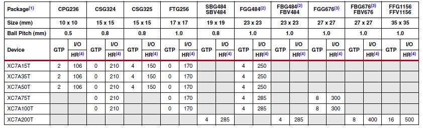
12 Xilinx 7 Series Families 12

13 Xilinx Artix-7 Family 13

14 Xilinx UltraScale Family Kintex and Virtex UltraScale and UltraScale+ 14
15 Xilinx: Basic CLB Architecture Look-up Table (LUT) implements truth table Memory elements: Flip-flop/latch Some - LUTs can also implement small RAMs Carry & control logic implements fast adders/subtractors Input[1:4] Control 4 LUT/ RAM Carry & Control Logic carry out Flip-flop/ Latch Output Q output clock, enable, set/reset 3 carry in 15
16 Combinational Logic Functions Gates are combined to create complex circuits A S Z Multiplexer example B If S = 0, Z = A If S = 1, Z = B Very common digital circuit Heavily used in S input controlled by configuration memory bit We ll see it again Truth table S A B Z Logic symbol A B S Z 16
17 Recall multiplexer example Configuration memory holds outputs for truth table Internal signals connect to control signals of multiplexers to select value of truth table for any given input value Look-up Tables B A S Z 1 Multiplexer A B S 0 1 Truth table S A B Z Z 17
18 Look-up Table Based RAMs Data In ck0 0 0 Normal LUT mode performs read operations Address decoder with write enable generates clock signals to latches for write operations Small RAMs but can be combined for larger RAMs In0 In1 In2 Address Decoder ck1 ck2 ck3 ck4 ck5 ck Z Write Enable ck7 1 1 In0 In1 In2 18
19 A Simple CLB Two 3-input LUTs Can implement any 4-input combinational logic function 1 flip-flop Programmable: Active levels Clock edge Set/reset 22 configuration memory bits 8 per LUT C0-7 S0-7 6 controls CB0-7 D2-0 D3 3 CB 5 Clock Enable Set/Reset Clock LUT C 8x1 LUT S 8x1 D2-0 LUT C 7 Smux 0 1 CB 0 CB 1 CB 2 C 6 C 5 C 4 C 3 C 2 C 1 C CEmux CB 3 SRmux 0 1 CB out FF CB 4 Cout SOmux 0 Sout 1 = Configuration Memory Bit 19
20 Artix-7 SLICEL (1/2 shown) Four 6-input Look-Up Tables (LUTs) Any combinational logic function of up to 6 inputs SLICEM LUT can function as small RAM (16x1-bit) or shift register (up to 16-bit) Example CLB Eight D flip-flops Programmable as latches Programmable clock edge, clock enable, set/reset Extra logic Fast carry for adders MUXs for Shannon expansion And more 20

21 CLBs and Slices in rows/columns 21
22 Using lookup-table (LUT) programmable logic 22
23 Functions of more variables than # of LUT inputs Shannon s Expansion Theorem (partition into smaller functions): ZZ aa, bb, cc, dd, ee, ff = aa ZZ 0, bb, cc, dd, ee, ff + aa ZZ 1, bb, cc, dd, ee, ff = aazz 0 + aazz 1 23
24 MM = SS 1 SS 0 II 0 + SS 1 SS 0 II 1 + SS 1 SS 0 II 2 + SS 1 SS 0 II 3 M1 M2 24
25 25
26 Fig Simplified Spartan and Virtex Slice 26
27 Bi-directional buffers Input/Output Cells Programmable for input or output Tri-state control for bi-directional operation Flip-flops/latches for improved timing Set-up and hold times Clock-to-output delay Pull-up/down resistors Routing resources Connections to core of array Programmable I/O voltage & current levels to/from internal routing resources Tri-state Control Output Data Input Data Pad 27
28 Detailed I/O Cell 28
29 Interconnect Network Wire segments of varying length xn = N CLBs in length 1, 2, 4, and 6 are most common xh = half the array in length xl = length of full array Programmable Interconnect Points (PIPs) Also known as Configurable Interconnect Points (CIPs) Transmission gate connects to 2 wire segments Controlled by configuration memory bit 0 = wires disconnected 1 = wires connected config bit Wire A Wire B 29
30 Xilinx interconnect structures 30
31 PIPs Break-point PIP Connect or isolate 2 wire segments Cross-point PIP Turn corners Multiplexer PIP Directional and buffered Select 1-of-N inputs for output Decoded MUX PIP N config bits select from 2 N inputs Non-decoded MUX PIP 1 config bit per input Compound cross-point PIP Collection of 6 break-point PIPs Can route to two isolated signal nets 31
32 32

33 Spartan 3 Routing Resources switch matrix over 2,400 PIPs mostly MUX PIPs PLB consists of 4 slices x6 wire segments x2 wire segments xh & xl wire segments over 450 total wire segments in PLB 33
34 Fully routed design LOGICIN1 S2BEG0 LOGICOUT1 (5,7) S3 (6,7) (7,7) S1 (8,7).I1.O1.O2 Net N1 LOGICOUT2 W2END0 W2BEG0 W2END1 W2BEG1 S2END0 LOGICIN2 (5,6) (6,6) (7,6) (8,6).I1 S2 E2BEG2 Net N2 E2END2 Net N1: Site S1 output pin O1 connects to input pin I1 on site S3 Net N2: Site S1 output pin O2 connects to input pin I1 on site S2 Black dots are routing pips Predefined connections exist between switch boxes 34

35 ELEC 4200 Lab 0 in Spartan 6 35
")
36 Lab 0 in Spartan 6 (routing details) 36
 INTs Nets CLBs IO")
37 Ex: modulo7 counter (device xc6slx25t) INTs Nets CLBs IO Pads 37
38 FPGA clock regions Logic Resources Logic Resources Clock Region Logic Resources Logic Resources Logic Resources Logic Resources Clock Region Logic Resources Logic Resources Center Clock Column(s) Clock Routing 38
39 Spartan 6 clock tree example Main vertical spine BUFG Folded vertical spine (one each in top and bottom half) CLKC tile Distribution wire in center of clock region Clock to INTs in one column 4 BUFH 7 8 INT CLEXM

40 7 Series FPGA high-level clock architecture view 40

41 Basic view of a clock region 41
42 Clock management tile (CMT) Mixed-mode clock manager (MMCM) MMCM Outputs Clock Sources MMCM Outputs = frequency divided, phase shifted, inverted Up to 24 CMTs per Series 7 device 42
43 Clock management tile (CMT) Phase-locked loop (PLL) PLL = frequency synthesizer using a voltage-controlled oscillator (VCO) PLL Outputs Clock Sources 43

44 From DCM/PLL and fabric Spartan 6 global clock sources From top edge global clock pads BUFGs Vertical spines BUFG controls from fabric Clock created by MIPS control logic Switch Box From right edge global clock pads From left edge Global clock pads From clock input pad From DCM/PLL and fabric From bottom edge global clock pads 44
45 Specialized hard cores RAMs single-port, dual-port, FIFOs 128 bits to 36K bits per RAM 4 to 575 RAM cores per FPGA DSPs 18x18-bit multiplier, 48-bit accumulator, etc. up to 512 per FPGA Microprocessors and/or microcontrollers Up to 2 per FPGA (hard core processor) Support soft core processors Synthesized from HDL into programmable resources Communication functions Gigabit transceivers Ethernet MAC PCE Express bus 45
46 FPGA Architectures 4000/Spartan NxN array of unit cells Unit cell = CLB + routing Special routing along center axes I/O cells around perimeter Virtex/Spartan-2 MxN array of unit cells Added block 4K RAMs at edges Virtex-2/Spartan-3 Block 18K RAMs in array Added 18x18 multipliers with each RAM Added PowerPCs in Virtex-2 Pro Virtex-4/Virtex-5 Added 48-bit DSP cores w/multipliers I/O cells along columns for BGA PC PC PC PC 46
47 Xilinx Virtex-4 Configuration memory: 4.7M to 50.8M bits of RAM PLBs: 1,536 to 22,272 4 slices per PLB 2 LUTs & 2 FFs per slice 2 slices can operate as RAMs/SRs Block RAMs: 48 to K-bit dualport RAMs Also operate as FIFOs DSP cores: 32 to 512, each includes: 18x18-bit multiplier 48-bit adder & accumulator Up to 2 PowerPC processors PC PC 47
48 Block RAMs 36 Kbit dual-port RAM Each port independently configurable: IK words x 36 bits 32 data bits + 4 parity bits 2K words x 18 bits 16 data bits + 2 parity bits 4K words x 9 bits 8 data bits + 1 parity bit 8K words x 4 bits (no parity) 16K words x 2 bits (no parity) 32K words x 1 bit (no parity) Each port has independently programmable clock edge, active levels for write enable, RAM enable, reset 48
49 49
50 ROM Contents 6-50
51 Distributed RAM 6-51
52 6-52
53 Refer to the synthesis guide for recommended HDL forms 53
54 DSP Blocks: Multiplier and Support Circuits 54
55 7 Series DSP48E1 DSP slice two s-complement multiplier: Dynamic bypass 48-bit accumulator: Can be used as a synchronous up/down counter Power-saving pre-adder: Optimizes symmetrical filter applications and reduces DSP slice requirements 55
56 DSP48E1 slice details 56

 ARM Processors in 7 Series SlicesPLBs Block RAMs Soft 233 MHz 274 69 3 MicroBlaze PowerPC")
57 Hard core Faster Fixed position Few devices Embedded Processors Soft core Slower Can be placed anywhere Applicable to many devices Virtex-4 Processors: Embedded Core Max Clock Processor Type Frequency PowerPC Hard 222 MHz Microblaze Soft 180 MHz Picoblaze Soft 221 MHz Picoblaze (optimized) ARM Processors in 7 Series SlicesPLBs Block RAMs Soft 233 MHz MicroBlaze PowerPC MicroBlaze PicoBlaze 57

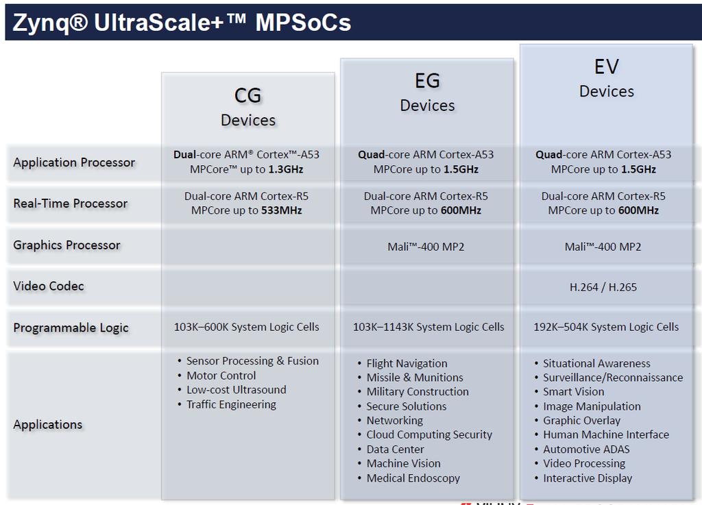
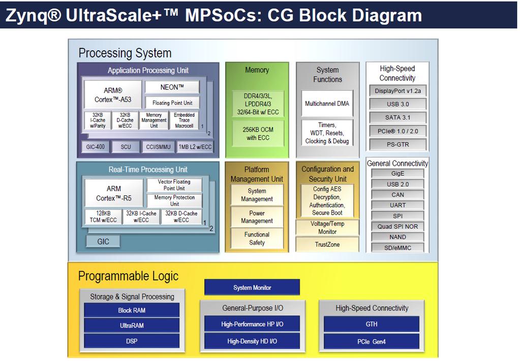
58 Xilinx Zynq SoC devices Zynq-7000 SoC: Dual-core ARM Cortex-A9 MPCore (up to 1GHz) Zynq UltraScale+ MPSoC: Quad-core ARM Cortex-A53 MP (up to 1.5 GHz) Dual-core ARM Cortex-R5 MPCore (up to 600MHz) GPY ARM Mali-400 MP2 (up to 667MHz) PL = Programmable Logic 58

59 Zynq-7000 SoC Features (1) Processing System Resources Continued next slide 59

60 Zynq-7000 SoC Features (2) Programmable Logic Resources 60
61 61

62 Zynq-7000 SoC Processor System 62
63 63
 64")
64 Zynq-7000 SoC Logic Fabric Series-7 CLBs, IOBs, etc. (as in Artix-7) 64
65 Configuration Interfaces Master FPGA retrieves its own configuration from ROM after power-up Serial or Parallel options clock CCLK CCLK CCLK Slave FPGA configured by external source (i.e., a µp) Serial or Parallel options Used for dynamic reconfiguration Can also read configuration memory contents Boundary Scan Interface 4-wire IEEE standard serial interface for testing Write and read access to configuration memory Not available in all Used for dynamic partial reconfiguration Interfaces to FPGA core Not available in all PROM with Configuration Data data out FPGA in Master Mode Connections between Boundary Scan Interface and internal routing network and PLBs (Xilinx provides 2-4 of these ports) Other configuration interfaces in some Din Dout FPGA in Slave Mode Din Dout FPGA in Slave Mode Din Dout 65
66 Slave configuration modes 66
 3.")
67 Nexys4 DDR configuration options Artix-7 100T bitstream is typically 30,606,304 bits USB-JTAG : PC connection via USB or JTAG 2. Master SPI: Program from quad mode flash memory (x1, x2, x4 width) 3. USB/SD: Program from micro SD card or USB memory stick 67
68 FPGA Configuration Memory PLB addressable Good for partial reconfiguration X-Y coordinates of PLB location to be written Requires tag to identify which resources will be configured Frame addressable Vertical or horizontal frame Access to all PLBs in frame Only portion of logic and routing resources accessible in a given frame Many frames to configure PLBs Major address for column, minor address for frame Hybrid, i.e.: Virtex-4 Virtex-5 Virtex-6 68
69 Daisy Chain Configuration EPROM Configuration Bits 69
70 Xilinx Configuration Interface Pins 70
71 Configuration Techniques Full configuration & readback Simple configuration interface Internal automatic calculation of frame address Long download time for large Partial reconfiguration & readback Only change portions of configuration memory with respect to reference design Reduces download time for reconfiguration Requires more complicated interface Command Register (CMR) Frame Length Register (FLR) Frame Address Register (FAR) Frame Data Register Input (FDRI) for download Output (FDRO) for readback (note separate access) 71
72 Full Configuration Example Dummy Word 0xFFFFFFFF Synchronize Word 0xAA CMD Write 0x Reset CRC 0x FLR Write 0x FLR = 0x Frame length = 37 words 1,184 bits 32 bits/word COR Write 0x COR Write 0x00003FE5 IDCODE Write 0x3001C001 Device ID = 0x0140D093 (3S50) MASK Write 0x3000C001 MASK = 0x CMD Write 0x Switch CCLK 0x FAR Write 0x FAR = 0x (full config) CMD Write 0x Write CFG 0x FDRI Write 0x # words to write 0x Xilinx ASCII Bitstream Created by Bitstream I.32 Design name: s3mod7.ncd Architecture: spartan3 Part: 3s50tq144 Date: Tue Sep 04 15:50: Bits: start of actual configuration data 72
FPGA Implementations
 FPGA Implementations Smith Text: Chapters 4-8 Online version at: http://www10.edacafe.com/book/asic/asics.php Topic outline Chapter 4 Programmable ASIC technologies Chapter 5 Programmable logic cells Chapter
Outline. Field Programmable Gate Arrays. Programming Technologies Architectures. Programming Interfaces. Historical perspective
 Outline Field Programmable Gate Arrays Historical perspective Programming Technologies Architectures PALs, PLDs,, and CPLDs FPGAs Programmable logic Interconnect network I/O buffers Specialized cores Programming
INTRODUCTION TO FIELD PROGRAMMABLE GATE ARRAYS (FPGAS)
") INTRODUCTION TO FIELD PROGRAMMABLE GATE ARRAYS (FPGAS) Bill Jason P. Tomas Dept. of Electrical and Computer Engineering University of Nevada Las Vegas FIELD PROGRAMMABLE ARRAYS Dominant digital design
INTRODUCTION TO FIELD PROGRAMMABLE GATE ARRAYS (FPGAS) Bill Jason P. Tomas Dept. of Electrical and Computer Engineering University of Nevada Las Vegas FIELD PROGRAMMABLE ARRAYS Dominant digital design
Outline of Presentation Field Programmable Gate Arrays (FPGAs(
 FPGA Architectures and Operation for Tolerating SEUs Chuck Stroud Electrical and Computer Engineering Auburn University Outline of Presentation Field Programmable Gate Arrays (FPGAs( FPGAs) How Programmable
FPGA for Complex System Implementation. National Chiao Tung University Chun-Jen Tsai 04/14/2011
 FPGA for Complex System Implementation National Chiao Tung University Chun-Jen Tsai 04/14/2011 About FPGA FPGA was invented by Ross Freeman in 1989 SRAM-based FPGA properties Standard parts Allowing multi-level
INTRODUCTION TO FPGA ARCHITECTURE
 3/3/25 INTRODUCTION TO FPGA ARCHITECTURE DIGITAL LOGIC DESIGN (BASIC TECHNIQUES) a b a y 2input Black Box y b Functional Schematic a b y a b y a b y 2 Truth Table (AND) Truth Table (OR) Truth Table (XOR)
Basic FPGA Architectures. Actel FPGAs. PLD Technologies: Antifuse. 3 Digital Systems Implementation Programmable Logic Devices
 3 Digital Systems Implementation Programmable Logic Devices Basic FPGA Architectures Why Programmable Logic Devices (PLDs)? Low cost, low risk way of implementing digital circuits as application specific
! Program logic functions, interconnect using SRAM. ! Advantages: ! Re-programmable; ! dynamically reconfigurable; ! uses standard processes.
 Topics! SRAM-based FPGA fabrics:! Xilinx.! Altera. SRAM-based FPGAs! Program logic functions, using SRAM.! Advantages:! Re-programmable;! dynamically reconfigurable;! uses standard processes.! isadvantages:!
EITF35: Introduction to Structured VLSI Design
 EITF35: Introduction to Structured VLSI Design Introduction to FPGA design Rakesh Gangarajaiah Rakesh.gangarajaiah@eit.lth.se Slides from Chenxin Zhang and Steffan Malkowsky WWW.FPGA What is FPGA? Field
Field Programmable Gate Array (FPGA)
") Field Programmable Gate Array (FPGA) Lecturer: Krébesz, Tamas 1 FPGA in general Reprogrammable Si chip Invented in 1985 by Ross Freeman (Xilinx inc.) Combines the advantages of ASIC and uc-based systems
Field Programmable Gate Array (FPGA) Lecturer: Krébesz, Tamas 1 FPGA in general Reprogrammable Si chip Invented in 1985 by Ross Freeman (Xilinx inc.) Combines the advantages of ASIC and uc-based systems
7-Series Architecture Overview
 7-Series Architecture Overview Zynq Vivado 2013.2 Version This material exempt per Department of Commerce license exception TSU Objectives After completing this module, you will be able to: Describe the
Today. Comments about assignment Max 1/T (skew = 0) Max clock skew? Comments about assignment 3 ASICs and Programmable logic Others courses
 Max clock skew? Comments about assignment 3 ASICs and Programmable logic Others courses") Today Comments about assignment 3-43 Comments about assignment 3 ASICs and Programmable logic Others courses octor Per should show up in the end of the lecture Mealy machines can not be coded in a single
Today Comments about assignment 3-43 Comments about assignment 3 ASICs and Programmable logic Others courses octor Per should show up in the end of the lecture Mealy machines can not be coded in a single
L2: FPGA HARDWARE : ADVANCED DIGITAL DESIGN PROJECT FALL 2015 BRANDON LUCIA
 L2: FPGA HARDWARE 18-545: ADVANCED DIGITAL DESIGN PROJECT FALL 2015 BRANDON LUCIA 18-545: FALL 2014 2 Admin stuff Project Proposals happen on Monday Be prepared to give an in-class presentation Lab 1 is
Programmable Logic Devices FPGA Architectures II CMPE 415. Overview This set of notes introduces many of the features available in the FPGAs of today.
 Overview This set of notes introduces many of the features available in the FPGAs of today. The majority use SRAM based configuration cells, which allows fast reconfiguation. Allows new design ideas to
Basic FPGA Architecture Xilinx, Inc. All Rights Reserved
 Basic FPGA Architecture 2005 Xilinx, Inc. All Rights Reserved Objectives After completing this module, you will be able to: Identify the basic architectural resources of the Virtex -II FPGA List the differences
Digital Integrated Circuits
 Digital Integrated Circuits Lecture 9 Jaeyong Chung Robust Systems Laboratory Incheon National University DIGITAL DESIGN FLOW Chung EPC6055 2 FPGA vs. ASIC FPGA (A programmable Logic Device) Faster time-to-market
Topics. Midterm Finish Chapter 7
 Lecture 9 Topics Midterm Finish Chapter 7 ROM (review) Memory device in which permanent binary information is stored. Example: 32 x 8 ROM Five input lines (2 5 = 32) 32 outputs, each representing a memory
Spiral 2-8. Cell Layout
 2-8.1 Spiral 2-8 Cell Layout 2-8.2 Learning Outcomes I understand how a digital circuit is composed of layers of materials forming transistors and wires I understand how each layer is expressed as geometric
EECS150 - Digital Design Lecture 6 - Field Programmable Gate Arrays (FPGAs)
") EECS150 - Digital Design Lecture 6 - Field Programmable Gate Arrays (FPGAs) September 12, 2002 John Wawrzynek Fall 2002 EECS150 - Lec06-FPGA Page 1 Outline What are FPGAs? Why use FPGAs (a short history
EECS150 - Digital Design Lecture 6 - Field Programmable Gate Arrays (FPGAs) September 12, 2002 John Wawrzynek Fall 2002 EECS150 - Lec06-FPGA Page 1 Outline What are FPGAs? Why use FPGAs (a short history
Outline. EECS150 - Digital Design Lecture 6 - Field Programmable Gate Arrays (FPGAs) FPGA Overview. Why FPGAs?
 FPGA Overview. Why FPGAs?") EECS150 - Digital Design Lecture 6 - Field Programmable Gate Arrays (FPGAs) September 12, 2002 John Wawrzynek Outline What are FPGAs? Why use FPGAs (a short history lesson). FPGA variations Internal logic
EECS150 - Digital Design Lecture 6 - Field Programmable Gate Arrays (FPGAs) September 12, 2002 John Wawrzynek Outline What are FPGAs? Why use FPGAs (a short history lesson). FPGA variations Internal logic
ECE 448 Lecture 5. FPGA Devices
 ECE 448 Lecture 5 FPGA Devices George Mason University Required reading Spartan-6 FPGA Configurable Logic Block: User Guide CLB Overview Slice Description 2 Recommended reading Highly recommended for the
FPGA architecture and design technology
 CE 435 Embedded Systems Spring 2017 FPGA architecture and design technology Nikos Bellas Computer and Communications Engineering Department University of Thessaly 1 FPGA fabric A generic island-style FPGA
EE219A Spring 2008 Special Topics in Circuits and Signal Processing. Lecture 9. FPGA Architecture. Ranier Yap, Mohamed Ali.
 EE219A Spring 2008 Special Topics in Circuits and Signal Processing Lecture 9 FPGA Architecture Ranier Yap, Mohamed Ali Annoucements Homework 2 posted Due Wed, May 7 Now is the time to turn-in your Hw
Very Large Scale Integration (VLSI)
") Very Large Scale Integration (VLSI) Lecture 6 Dr. Ahmed H. Madian Ah_madian@hotmail.com Dr. Ahmed H. Madian-VLSI 1 Contents FPGA Technology Programmable logic Cell (PLC) Mux-based cells Look up table PLA
Very Large Scale Integration (VLSI) Lecture 6 Dr. Ahmed H. Madian Ah_madian@hotmail.com Dr. Ahmed H. Madian-VLSI 1 Contents FPGA Technology Programmable logic Cell (PLC) Mux-based cells Look up table PLA
Outline of Presentation
 Built-In Self-Test for Programmable I/O Buffers in FPGAs and SoCs Sudheer Vemula and Charles Stroud Electrical and Computer Engineering Auburn University presented at 2006 IEEE Southeastern Symp. On System
CPE/EE 422/522. Introduction to Xilinx Virtex Field-Programmable Gate Arrays Devices. Dr. Rhonda Kay Gaede UAH. Outline
 CPE/EE 422/522 Introduction to Xilinx Virtex Field-Programmable Gate Arrays Devices Dr. Rhonda Kay Gaede UAH Outline Introduction Field-Programmable Gate Arrays Virtex Virtex-E, Virtex-II, and Virtex-II
Altera FLEX 8000 Block Diagram
 Altera FLEX 8000 Block Diagram Figure from Altera technical literature FLEX 8000 chip contains 26 162 LABs Each LAB contains 8 Logic Elements (LEs), so a chip contains 208 1296 LEs, totaling 2,500 16,000
FPGA Architecture Overview. Generic FPGA Architecture (1) FPGA Architecture
 FPGA Architecture") FPGA Architecture Overview dr chris dick dsp chief architect wireless and signal processing group xilinx inc. Generic FPGA Architecture () Generic FPGA architecture consists of an array of logic tiles
FPGA Architecture Overview dr chris dick dsp chief architect wireless and signal processing group xilinx inc. Generic FPGA Architecture () Generic FPGA architecture consists of an array of logic tiles
Memory and Programmable Logic
 Digital Circuit Design and Language Memory and Programmable Logic Chang, Ik Joon Kyunghee University Memory Classification based on functionality ROM : Read-Only Memory RWM : Read-Write Memory RWM NVRWM
FPGA. Logic Block. Plessey FPGA: basic building block here is 2-input NAND gate which is connected to each other to implement desired function.
 FPGA Logic block of an FPGA can be configured in such a way that it can provide functionality as simple as that of transistor or as complex as that of a microprocessor. It can used to implement different
FPGA: What? Why? Marco D. Santambrogio
 FPGA: What? Why? Marco D. Santambrogio marco.santambrogio@polimi.it 2 Reconfigurable Hardware Reconfigurable computing is intended to fill the gap between hardware and software, achieving potentially much
Zynq-7000 All Programmable SoC Product Overview
 Zynq-7000 All Programmable SoC Product Overview The SW, HW and IO Programmable Platform August 2012 Copyright 2012 2009 Xilinx Introducing the Zynq -7000 All Programmable SoC Breakthrough Processing Platform
Programmable Logic. Any other approaches?
 Programmable Logic So far, have only talked about PALs (see 22V10 figure next page). What is the next step in the evolution of PLDs? More gates! How do we get more gates? We could put several PALs on one
Synthesis of VHDL Code for FPGA Design Flow Using Xilinx PlanAhead Tool
 Synthesis of VHDL Code for FPGA Design Flow Using Xilinx PlanAhead Tool Md. Abdul Latif Sarker, Moon Ho Lee Division of Electronics & Information Engineering Chonbuk National University 664-14 1GA Dekjin-Dong
FPGA How do they work?
 ent FPGA How do they work? ETI135, Advanced Digital IC Design What is a FPGA? Manufacturers Distributed RAM History FPGA vs ASIC FPGA and Microprocessors Alternatives to FPGAs Anders Skoog, Stefan Granlund
Zynq AP SoC Family
 Programmable Logic (PL) Processing System (PS) Zynq -7000 AP SoC Family Cost-Optimized Devices Mid-Range Devices Device Name Z-7007S Z-7012S Z-7014S Z-7010 Z-7015 Z-7020 Z-7030 Z-7035 Z-7045 Z-7100 Part
International Training Workshop on FPGA Design for Scientific Instrumentation and Computing November 2013.
 2499-1 International Training Workshop on FPGA Design for Scientific Instrumentation and Computing 11-22 November 2013 FPGA Introduction Cristian SISTERNA National University of San Juan San Juan Argentina
Learning Outcomes. Spiral 3 1. Digital Design Targets ASICS & FPGAS REVIEW. Hardware/Software Interfacing
 3-. 3-.2 Learning Outcomes Spiral 3 Hardware/Software Interfacing I understand the PicoBlaze bus interface signals: PORT_ID, IN_PORT, OUT_PORT, WRITE_STROBE I understand how a memory map provides the agreement
Virtex-II Architecture. Virtex II technical, Design Solutions. Active Interconnect Technology (continued)
") Virtex-II Architecture SONET / SDH Virtex II technical, Design Solutions PCI-X PCI DCM Distri RAM 18Kb BRAM Multiplier LVDS FIFO Shift Registers BLVDS SDRAM QDR SRAM Backplane Rev 4 March 4th. 2002 J-L
Virtex-II Architecture SONET / SDH Virtex II technical, Design Solutions PCI-X PCI DCM Distri RAM 18Kb BRAM Multiplier LVDS FIFO Shift Registers BLVDS SDRAM QDR SRAM Backplane Rev 4 March 4th. 2002 J-L
Introduction to Field Programmable Gate Arrays
 Introduction to Field Programmable Gate Arrays Lecture 1/3 CERN Accelerator School on Digital Signal Processing Sigtuna, Sweden, 31 May 9 June 2007 Javier Serrano, CERN AB-CO-HT Outline Historical introduction.
Spiral 3-1. Hardware/Software Interfacing
 3-1.1 Spiral 3-1 Hardware/Software Interfacing 3-1.2 Learning Outcomes I understand the PicoBlaze bus interface signals: PORT_ID, IN_PORT, OUT_PORT, WRITE_STROBE I understand how a memory map provides
Copyright 2017 Xilinx.
 All Programmable Automotive SoC Comparison XA Zynq UltraScale+ MPSoC ZU2/3EG, ZU4/5EV Devices XA Zynq -7000 SoC Z-7010/7020/7030 Devices Application Processor Real-Time Processor Quad-core ARM Cortex -A53
EE178 Lecture Module 2. Eric Crabill SJSU / Xilinx Fall 2007
 EE178 Lecture Module 2 Eric Crabill SJSU / Xilinx Fall 2007 Lecture #4 Agenda Survey of implementation technologies. Implementation Technologies Small scale and medium scale integration. Up to about 200
Field Programmable Gate Array
 Field Programmable Gate Array System Arch 27 (Fire Tom Wada) What is FPGA? System Arch 27 (Fire Tom Wada) 2 FPGA Programmable (= reconfigurable) Digital System Component Basic components Combinational
Embedded Systems: Hardware Components (part I) Todor Stefanov
 Todor Stefanov") Embedded Systems: Hardware Components (part I) Todor Stefanov Leiden Embedded Research Center Leiden Institute of Advanced Computer Science Leiden University, The Netherlands Outline Generic Embedded System
Embedded Systems: Hardware Components (part I) Todor Stefanov Leiden Embedded Research Center Leiden Institute of Advanced Computer Science Leiden University, The Netherlands Outline Generic Embedded System
Introduction to FPGAs. H. Krüger Bonn University
 Introduction to FPGAs H. Krüger Bonn University Outline 1. History 2. FPGA Architecture 3. Current Trends 4. Design Methodology (short see other lectures) Disclaimer: Most of the resources used for this
What is Xilinx Design Language?
 Bill Jason P. Tomas University of Nevada Las Vegas Dept. of Electrical and Computer Engineering What is Xilinx Design Language? XDL is a human readable ASCII format compatible with the more widely used
Evolution of Implementation Technologies. ECE 4211/5211 Rapid Prototyping with FPGAs. Gate Array Technology (IBM s) Programmable Logic
 Programmable Logic") ECE 42/52 Rapid Prototyping with FPGAs Dr. Charlie Wang Department of Electrical and Computer Engineering University of Colorado at Colorado Springs Evolution of Implementation Technologies Discrete devices:
ECE 42/52 Rapid Prototyping with FPGAs Dr. Charlie Wang Department of Electrical and Computer Engineering University of Colorado at Colorado Springs Evolution of Implementation Technologies Discrete devices:
ECE 636. Reconfigurable Computing. Lecture 2. Field Programmable Gate Arrays I
 ECE 636 Reconfigurable Computing Lecture 2 Field Programmable Gate Arrays I Overview Anti-fuse and EEPROM-based devices Contemporary SRAM devices - Wiring - Embedded New trends - Single-driver wiring -
XA Spartan-6 Automotive FPGA Family Overview
 10 XA Spartan-6 Automotive FPGA Family Overview Product Specification General Description The Xilinx Automotive (XA) Spartan -6 family of FPGAs provides leading system integration capabilities with the
Introduction to Partial Reconfiguration Methodology
 Methodology This material exempt per Department of Commerce license exception TSU Objectives After completing this module, you will be able to: Define Partial Reconfiguration technology List common applications
Atmel AT94K FPSLIC Architecture Field Programmable Gate Array
 Embedded Processor Based Built-In Self-Test and Diagnosis of FPGA Core in FPSLIC John Sunwoo (Logic BIST) Srinivas Garimella (RAM BIST) Sudheer Vemula (I/O Cell BIST) Chuck Stroud (Routing BIST) Jonathan
ECE 545 Lecture 12. FPGA Resources. George Mason University
 ECE 545 Lecture 2 FPGA Resources George Mason University Recommended reading 7 Series FPGAs Configurable Logic Block: User Guide Overview Functional Details 2 What is an FPGA? Configurable Logic Blocks
Programmable Logic. Simple Programmable Logic Devices
 Programmable Logic SM098 Computation Structures - Programmable Logic Simple Programmable Logic evices Programmable Array Logic (PAL) AN-OR arrays are common blocks in SPL and CPL architectures Implements
ECE 448 Lecture 5. FPGA Devices
 E 448 Lecture 5 FPGA evices E 448 FPGA and ASIC esign with VHL George Mason University Required reading 7 Series FPGAs Configurable Logic Block: User Guide Overview Functional etails 2 What is an FPGA?
Memory and Programmable Logic
 Memory and Programmable Logic Memory units allow us to store and/or retrieve information Essentially look-up tables Good for storing data, not for function implementation Programmable logic device (PLD),
CHAPTER 9 MULTIPLEXERS, DECODERS, AND PROGRAMMABLE LOGIC DEVICES
 CHAPTER 9 MULTIPLEXERS, DECODERS, AND PROGRAMMABLE LOGIC DEVICES This chapter in the book includes: Objectives Study Guide 9.1 Introduction 9.2 Multiplexers 9.3 Three-State Buffers 9.4 Decoders and Encoders
VHX - Xilinx - FPGA Programming in VHDL
 Training Xilinx - FPGA Programming in VHDL: This course explains how to design with VHDL on Xilinx FPGAs using ISE Design Suite - Programming: Logique Programmable VHX - Xilinx - FPGA Programming in VHDL
The Xilinx XC6200 chip, the software tools and the board development tools
 The Xilinx XC6200 chip, the software tools and the board development tools What is an FPGA? Field Programmable Gate Array Fully programmable alternative to a customized chip Used to implement functions
FPGAs: Instant Access
 FPGAs: Instant Access Clive"Max"Maxfield AMSTERDAM BOSTON HEIDELBERG LONDON NEW YORK OXFORD PARIS SAN DIEGO SAN FRANCISCO SINGAPORE SYDNEY TOKYO % ELSEVIER Newnes is an imprint of Elsevier Newnes Contents
Zynq Architecture, PS (ARM) and PL
 and PL") , PS (ARM) and PL Joint ICTP-IAEA School on Hybrid Reconfigurable Devices for Scientific Instrumentation Trieste, 1-5 June 2015 Fernando Rincón Fernando.rincon@uclm.es 1 Contents Zynq All Programmable
, PS (ARM) and PL Joint ICTP-IAEA School on Hybrid Reconfigurable Devices for Scientific Instrumentation Trieste, 1-5 June 2015 Fernando Rincón Fernando.rincon@uclm.es 1 Contents Zynq All Programmable
Field Program mable Gate Arrays
 Field Program mable Gate Arrays M andakini Patil E H E P g r o u p D H E P T I F R SERC school NISER, Bhubaneshwar Nov 7-27 2017 Outline Digital electronics Short history of programmable logic devices
Chapter 2. FPGA and Dynamic Reconfiguration ...
 Chapter 2 FPGA and Dynamic Reconfiguration... This chapter will introduce a family of silicon devices, FPGAs exploring their architecture. This work is based on these particular devices. The chapter will
The Next Generation 65-nm FPGA. Steve Douglass, Kees Vissers, Peter Alfke Xilinx August 21, 2006
 The Next Generation 65-nm FPGA Steve Douglass, Kees Vissers, Peter Alfke Xilinx August 21, 2006 Hot Chips, 2006 Structure of the talk 65nm technology going towards 32nm Virtex-5 family Improved I/O Benchmarking
Summary. Introduction. Application Note: Virtex, Virtex-E, Spartan-IIE, Spartan-3, Virtex-II, Virtex-II Pro. XAPP152 (v2.1) September 17, 2003
 September 17, 2003") Application Note: Virtex, Virtex-E, Spartan-IIE, Spartan-3, Virtex-II, Virtex-II Pro Xilinx Tools: The Estimator XAPP152 (v2.1) September 17, 2003 Summary This application note is offered as complementary
Application Note: Virtex, Virtex-E, Spartan-IIE, Spartan-3, Virtex-II, Virtex-II Pro Xilinx Tools: The Estimator XAPP152 (v2.1) September 17, 2003 Summary This application note is offered as complementary
Built-In Self-Test for Programmable I/O Buffers in FPGAs and SoCs
 Built-In Self-Test for Programmable I/O Buffers in FPGAs and SoCs Sudheer Vemula, Student Member, IEEE, and Charles Stroud, Fellow, IEEE Abstract The first Built-In Self-Test (BIST) approach for the programmable
PROGRAMMABLE MODULES SPECIFICATION OF PROGRAMMABLE COMBINATIONAL AND SEQUENTIAL MODULES
 PROGRAMMABLE MODULES SPECIFICATION OF PROGRAMMABLE COMBINATIONAL AND SEQUENTIAL MODULES. psa. rom. fpga THE WAY THE MODULES ARE PROGRAMMED NETWORKS OF PROGRAMMABLE MODULES EXAMPLES OF USES Programmable
A Case Study. Jonathan Harris, and Jared Phillips Dept. of Electrical and Computer Engineering Auburn University
 Built-In Self-Test for System-on on-chip: A Case Study Charles Stroud, Srinivas Garimella,, John Sunwoo, Jonathan Harris, and Jared Phillips Dept. of Electrical and Computer Engineering Auburn University
Reconfigurable Computing
 Reconfigurable Computing FPGA Architecture Architecture should speak of its time and place, but yearn for timelessness. Frank Gehry Philip Leong (philip.leong@sydney.edu.au) School of Electrical and Information
Experiment 3. Digital Circuit Prototyping Using FPGAs
 Experiment 3. Digital Circuit Prototyping Using FPGAs Masud ul Hasan Muhammad Elrabaa Ahmad Khayyat Version 151, 11 September 2015 Table of Contents 1. Objectives 2. Materials Required 3. Background 3.1.
High Capacity and High Performance 20nm FPGAs. Steve Young, Dinesh Gaitonde August Copyright 2014 Xilinx
 High Capacity and High Performance 20nm FPGAs Steve Young, Dinesh Gaitonde August 2014 Not a Complete Product Overview Page 2 Outline Page 3 Petabytes per month Increasing Bandwidth Global IP Traffic Growth
Enabling success from the center of technology. A Practical Guide to Configuring the Spartan-3A Family
 A Practical Guide to Configuring the Spartan-3A Family Goals 2 Explain advantages and disadvantages of each configuration mechanism available for Spartan-3A Show how to use an industry standard flash for
Field Programmable Gate Arrays (FPGAs)
") EECE-474 Advanced VHDL and FPGA Design Lecture Field Programmable Gate Arrays (FPGAs) Cristinel Ababei Dept. of Electrical and Computer Engr. Marquette University Overview FPGA Devices ASIC vs. FPGA FPGA
EECE-474 Advanced VHDL and FPGA Design Lecture Field Programmable Gate Arrays (FPGAs) Cristinel Ababei Dept. of Electrical and Computer Engr. Marquette University Overview FPGA Devices ASIC vs. FPGA FPGA
System-on Solution from Altera and Xilinx
 System-on on-a-programmable-chip Solution from Altera and Xilinx Xun Yang VLSI CAD Lab, Computer Science Department, UCLA FPGAs with Embedded Microprocessors Combination of embedded processors and programmable
Configuration Modes and Daisy-Chains
 Application Note: Spartan-II Family XAPP176 (v0.9) December 4, 1999 Spartan-II FPGA Family Configuration and eadback Application Note Summary This application note is offered as complementary text to the
Lecture 7. Standard ICs FPGA (Field Programmable Gate Array) VHDL (Very-high-speed integrated circuits. Hardware Description Language)
 VHDL (Very-high-speed integrated circuits. Hardware Description Language)") Standard ICs FPGA (Field Programmable Gate Array) VHDL (Very-high-speed integrated circuits Hardware Description Language) 1 Standard ICs PLD: Programmable Logic Device CPLD: Complex PLD FPGA: Field Programmable
Standard ICs FPGA (Field Programmable Gate Array) VHDL (Very-high-speed integrated circuits Hardware Description Language) 1 Standard ICs PLD: Programmable Logic Device CPLD: Complex PLD FPGA: Field Programmable
Section 6. Memory Components Chapter 5.7, 5.8 Physical Implementations Chapter 7 Programmable Processors Chapter 8
 Section 6 Memory Components Chapter 5.7, 5.8 Physical Implementations Chapter 7 Programmable Processors Chapter 8 Types of memory Two major types of memory Volatile When power to the device is removed
DIGITAL CIRCUIT LOGIC UNIT 9: MULTIPLEXERS, DECODERS, AND PROGRAMMABLE LOGIC DEVICES
 DIGITAL CIRCUIT LOGIC UNIT 9: MULTIPLEXERS, DECODERS, AND PROGRAMMABLE LOGIC DEVICES 1 Learning Objectives 1. Explain the function of a multiplexer. Implement a multiplexer using gates. 2. Explain the
Xilinx ASMBL Architecture
 FPGA Structure Xilinx ASMBL Architecture Design Flow Synthesis: HDL to FPGA primitives Translate: FPGA Primitives to FPGA Slice components Map: Packing of Slice components into Slices, placement of Slices
Copyright 2016 Xilinx
 Zynq Architecture Zynq Vivado 2015.4 Version This material exempt per Department of Commerce license exception TSU Objectives After completing this module, you will be able to: Identify the basic building
XA Artix-7 FPGAs Data Sheet: Overview
 10 XA Artix-7 FPGAs Data Sheet: Overview Product Specification General Description Xilinx XA Artix -7 (Automotive) FPGAs are optimized for the lowest cost and power with small form-factor packaging for
ECE 645: Lecture 1. Basic Adders and Counters. Implementation of Adders in FPGAs
 ECE 645: Lecture Basic Adders and Counters Implementation of Adders in FPGAs Required Reading Behrooz Parhami, Computer Arithmetic: Algorithms and Hardware Design Chapter 5, Basic Addition and Counting,
Spartan-3E FPGA Design Guide for prototyping and production environment
 3ème conférence Internationale des énergies renouvelables CIER-2015 Proceedings of Engineering and Technology - PET Spartan-3E FPGA Design Guide for prototyping and production environment Mohammed BOUDJEMA
Keywords: Soft Core Processor, Arithmetic and Logical Unit, Back End Implementation and Front End Implementation.
 ISSN 2319-8885 Vol.03,Issue.32 October-2014, Pages:6436-6440 www.ijsetr.com Design and Modeling of Arithmetic and Logical Unit with the Platform of VLSI N. AMRUTHA BINDU 1, M. SAILAJA 2 1 Dept of ECE,
Chapter 13 Programmable Logic Device Architectures
 Chapter 13 Programmable Logic Device Architectures Chapter 13 Objectives Selected areas covered in this chapter: Describing different categories of digital system devices. Describing different types of
Embedded Systems. 7. System Components
 Embedded Systems 7. System Components Lothar Thiele 7-1 Contents of Course 1. Embedded Systems Introduction 2. Software Introduction 7. System Components 10. Models 3. Real-Time Models 4. Periodic/Aperiodic
Built-In Self-Test for Regular Structure Embedded Cores in System-on-Chip
 Built-In Self-Test for Regular Structure Embedded Cores in System-on-Chip Srinivas Murthy Garimella Master s Thesis Defense Thesis Advisor: Dr. Charles E. Stroud Committee Members: Dr. Victor P. Nelson
Virtex-II Architecture
 Virtex-II Architecture Block SelectRAM resource I/O Blocks (IOBs) edicated multipliers Programmable interconnect Configurable Logic Blocks (CLBs) Virtex -II architecture s core voltage operates at 1.5V
Virtex-4 Family Overview
 Virtex-4 User Guide 0 Virtex-4 Family Overview DS112 (v1.1) September 10, 2004 0 0 General Description The Virtex-4 Family is the newest generation FPGA from Xilinx. The innovative Advanced Silicon Modular
An Architecture for Fail-Silent Operation of FPGAs and Configurable SoCs
 An Architecture for Fail-Silent Operation of FPGAs and Configurable SoCs Lee W. Lerner and Charles E. Stroud Dept. of Electrical and Computer Engineering Auburn University Auburn, AL, USA Abstract We present
Advanced Digital Design Using FPGA. Dr. Shahrokh Abadi
 Advanced Digital Design Using FPGA Dr. Shahrokh Abadi 1 Venue Computer Lab: Tuesdays 10 12 am (Fixed) Computer Lab: Wednesday 10-12 am (Every other odd weeks) Note: Due to some unpredicted problems with
Spartan-3 FPGA Family Advanced Configuration Architecture
 Application Note: Spartan-3 Family R XAPP452 (v1.1) June 25, 2008 Spartan-3 FPGA Family Advanced Configuration Architecture Summary This application note provides a detailed description of the Spartan
Hardware Design with VHDL PLDs IV ECE 443
 Embedded Processor Cores (Hard and Soft) Electronic design can be realized in hardware (logic gates/registers) or software (instructions executed on a microprocessor). The trade-off is determined by how
Lecture 11 SRAM Zhuo Feng. Z. Feng MTU EE4800 CMOS Digital IC Design & Analysis 2010
 EE4800 CMOS Digital IC Design & Analysis Lecture 11 SRAM Zhuo Feng 11.1 Memory Arrays SRAM Architecture SRAM Cell Decoders Column Circuitryit Multiple Ports Outline Serial Access Memories 11.2 Memory Arrays
PS2 VGA Peripheral Based Arithmetic Application Using Micro Blaze Processor
 PS2 VGA Peripheral Based Arithmetic Application Using Micro Blaze Processor K.Rani Rudramma 1, B.Murali Krihna 2 1 Assosiate Professor,Dept of E.C.E, Lakireddy Bali Reddy Engineering College, Mylavaram
Qsys and IP Core Integration
 Qsys and IP Core Integration Stephen A. Edwards (after David Lariviere) Columbia University Spring 2016 IP Cores Altera s IP Core Integration Tools Connecting IP Cores IP Cores Cyclone V SoC: A Mix of
FPGA. Agenda 11/05/2016. Scheduling tasks on Reconfigurable FPGA architectures. Definition. Overview. Characteristics of the CLB.
 Agenda The topics that will be addressed are: Scheduling tasks on Reconfigurable FPGA architectures Mauro Marinoni ReTiS Lab, TeCIP Institute Scuola superiore Sant Anna - Pisa Overview on basic characteristics
PINE TRAINING ACADEMY
 PINE TRAINING ACADEMY Course Module A d d r e s s D - 5 5 7, G o v i n d p u r a m, G h a z i a b a d, U. P., 2 0 1 0 1 3, I n d i a Digital Logic System Design using Gates/Verilog or VHDL and Implementation
FPGA Based Digital Design Using Verilog HDL
 FPGA Based Digital Design Using Course Designed by: IRFAN FAISAL MIR ( Verilog / FPGA Designer ) irfanfaisalmir@yahoo.com * Organized by Electronics Division Integrated Circuits Uses for digital IC technology
Soft-Core Embedded Processor-Based Built-In Self- Test of FPGAs: A Case Study
 Soft-Core Embedded Processor-Based Built-In Self- Test of FPGAs: A Case Study Bradley F. Dutton, Graduate Student Member, IEEE, and Charles E. Stroud, Fellow, IEEE Dept. of Electrical and Computer Engineering