Learning Outcomes. Spiral 3 1. Digital Design Targets ASICS & FPGAS REVIEW. Hardware/Software Interfacing
|
|
|
- Violet Higgins
- 5 years ago
- Views:
Transcription


1 Learning Outcomes Spiral 3 Hardware/Software Interfacing I understand the PicoBlaze bus interface signals: PORT_ID, IN_PORT, OUT_PORT, WRITE_STROBE I understand how a memory map provides the agreement between addresses the software will use and that the hardware must recognize and respond to I understand how to build address decoding logic to ensure only the appropriate value/register is selected for a given PORTID For output, I can take a memory map and the PORTID and OUTDATA bits such that the appropriate data is input or saved in a register when an OUTPUT instruction is executed For input, I can take a memory map and the appropriate PORTID bits to build logic and muxes such that the appropriate data value is present at INDATA when an INPUT instruction is executed Mark Redekopp Digital Design Targets Two possible implementation targets Custom Chips (ASIC s = Application Specific Integrated Circuits): Physical gates are created on silicon to implement particular design FPGA (Field Programmable Gate Array s): Programmable logic using programmable memories to implement logic functions along with other logic resources tiled on the chip. Can implement any design and then be changed to implement a new one ASICS & FPGAS REVIEW In an ASIC design, a unique chip will be manufactured that implements our design at which point the HW design is fixed & cannot be changed (example: Pentium, etc.) FPGA s have logic resources on them that we can configure to implement our specific design. We can then reconfigure it to implement another design

 Final netlist is sent to chip maker for production Fabrication is very expensive (> $ million) so get your")

 FPGA")
2 ASICs Implementation ASIC s Use the CAD tools to synthesize and route a netlist Synthesis = Takes logic description or logic schematic & converts to transistor level gates Place and Route = Figure out where each gate should go on the chip) Final netlist is sent to chip maker for production Fabrication is very expensive (> $ million) so get your design right the first time. FPGA s Synthesis converts logic description to necessary LUT contents, etc. Place and route produces a configuration for the FPGA chip Can reconfigure FPGA as much as you like, so less important to get it right st time ASIC s vs. FPGA s Xilinx Spartan 3E ASIC s Handles Designs Expensive Flexible (Cannot be to perform a new hardware function) FPGA s Designs Expensive Flexible Digilent Nexys 2 Board Has a Xilinx Spartan 3E FPGA (XC3S5e) 5K gate equivalent 932 D FF s on board On board I/O (4) 7 Segment Displays () LED s (4) Push Buttons () Switches
![Latest FPGA's 3-.9 3-. SoC design (Xilinx Kintex [KU5]) Quad Core ARM cores DDR3 SDRAM Memory Interface ~ I/O Pins Equiv.](/docs-images/93/112605166/images/3-0.jpg "~5M gate equivalent FPGA fabric ~M D FFs + 552K LUTs 96 dedicated DSP \"slices\" x multiply + adder 34.")
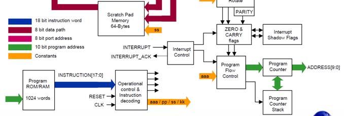
3 Latest FPGA's SoC design (Xilinx Kintex [KU5]) Quad Core ARM cores DDR3 SDRAM Memory Interface ~ I/O Pins Equiv. ~5M gate equivalent FPGA fabric ~M D FFs + 552K LUTs 96 dedicated DSP "slices" x multiply + adder 34.6 Megabits of onboard Block RAMs Hardware/Software Interfacing PICOBLAZE Input / Output The processor connects to peripherals and other logic via the (address, data, and control) Software running on the processor performs and that read and write data to and from these devices based on Processor Memory FE may signify a white dot at a particular location Video Interface 254 A D C 254 WRITE 399 Keyboard Interface 3-. Introduction Picoblaze (aka KCPSM3) is an bit The processor is not implemented directly in hardware on the FPGA but instead is just a description that is then using the same process as any of our other designs It provides a bus interface that can be connected to custom logic that you design and then used to control that custom logic via executing on the processor


4 Input / Output Operations 3-.6
5 Exercise Remember: Registers w/ Enables Make the register below capture data (out_data) from your Picoblaze whenever it outputs address FF hex on (address or port_id) Registers (D FF s) will sample the D bit every clock edge and pass it to Q Sometimes we may want to hold the value of Q and ignore D even at a clock edge We can add an enable input and some logic in front of the D FF to accomplish this D /AR Y S SET D Q CLR FF with Data Enable Q Picoblaze Processor (software controlled) WS (W) D[7:] Q[7:] Reg RST /AR D i Q i * X X X, X X Q i X Q i Registers w/ Enables Recall Memory Interfaces The D value is sampled at the clock edge only if the enable is active Otherwise the current Q value is maintained /AR D[3:] Q[3:] We provide address and data = Overall enable (unless it is ) the memory won't read or write (we assume =) W = Write enable = Write / = read A[2:] DI[3:] W A[2:] DI[3:] W twrite M[3] DO[3:] DO[3:]??? mem[3] = mem[6] = Assume = tacc
6 Exercise Exercise 2 Make the register below capture data (out_data) from your Picoblaze whenever it outputs address FF hex on (address or port_id) Use your PicoBlaze to receive input from A given address hex and B for address x hex Picoblaze Processor (software controlled) WS (W) D[7:] Q[7:] Reg RST A[7:] B[7:] Picoblaze Processor (software controlled) WS (W) Memory Maps A memory map shows what devices are assigned to a given or address range that can then be accessed by the processor (and its software programs) Memory Maps Given an bit address space (256 locations) and 3 devices that we want to interface to our microprocessor, we first must create the memory map A 64 bytes (64x) memory A single bit register A single bit D FF Dec A7 A6 A5 A4 A3 A2 A A Assigned Device Input Switches LEDs Seg Display Dec A7 A6 A5 A4 A3 A2 A A Assigned Device 64x Memory bit Register 2 bit D FF
7 Memory Maps Exercise: What is a minimal set of bits that could be used to distinguish each device from the others? A 64 bytes (64x) memory => A single bit register => A single bit D FF => Dec A7 A6 A5 A4 A3 A2 A A Assigned Device 64x Memory bit Register 2 bit D FF Memory Aliasing Given A 64 bytes (64x) memory => A single bit register => A single bit D FF => By using don't care situations the bit register will respond to address where A7 A6 = (i.e. ) and similarly the bit D FF will respond to any address where A7= (i.e. ) Dec A7 A6 A5 A4 A3 A2 A A Assigned Device 64x Memory bit Register 2 bit D FF Address Decoding Address decoding refers to the process of the correct device based on a specific address 2 3 S S Picoblaze Processor (software controlled) WS (W) 64x Memory DI[7:] DO[7:] 6 A[5:] W -bit REG D[7:] Q[7:] RST SET D Q -bit DFF CLR Memory Maps Exercise: Repeat the exercise to find a minimal set of bits that could be used to distinguish each device from the others? A 64 bytes (64x) memory => A single bit register => A single bit D FF => Dec A7 A6 A5 A4 A3 A2 A A Assigned Device bit Register bit D FF 2 64x 3 Memory
8 Address Decoding Exercise 2 High Order Interleaving 64x Memory DI[7:] DO[7:] 6 A[5:] General strategy is to place devices at ranges of address divide by more significant bits 2 3 S S Picoblaze Processor (software controlled) WS (W) W -bit REG D[7:] Q[7:] RST SET D Q -bit DFF CLR Dec A7 A6 A5 A4 A3 A2 A A Assigned Device 64x Memory bit Register bit D FF PING))) Interfacing Interface the PING))) engine you created to the Picoblaze processor PICOBLAZE ASSEMBLY
,, (9 ) Pages 6 36, focus on OUTPUT 34 INPUT 35 SHIFTS 32,33 JUMP 7 LOAD 22 COMPARE 3")
 of xff 3-.35 3-.")
9 Relevant Manual Pages Pages 4 6, (7),, (9 ) Pages 6 36, focus on OUTPUT 34 INPUT 35 SHIFTS 32,33 JUMP 7 LOAD 22 COMPARE 3 Input/Output design 65 6 Output Instruction Example: output s, FF Outputs the bit number in s as data on out_port to the address (port_id) of xff Input Instruction LOAD Instruction Example: input s, c Places the address xc on the port_id and then grabs data from the in_port at the end of the second cycle and writes it into register s Example: load s3, a5 Loads the constant xa5 into register s3


10 Compare Instruction AND Instruction 3-.3 Example: compare sf, 2a Compares the data in register sf to the hex constant x2a. It sets the Z flag (to determine equality) and C flag (to indicate less than) Example: and s3, 4 Takes the bitwise AND of the data in register s3 and the hex constant x4, overwriting s3 with the result. It sets the Z flag if the result of the ANDing is Jump Instruction Example: jump Z, label Jumps to the location specified by label if the condition bit (Z) is true
Spiral 3-1. Hardware/Software Interfacing
 3-1.1 Spiral 3-1 Hardware/Software Interfacing 3-1.2 Learning Outcomes I understand the PicoBlaze bus interface signals: PORT_ID, IN_PORT, OUT_PORT, WRITE_STROBE I understand how a memory map provides
Learning Outcomes. Input / Output. Introduction PICOBLAZE 10/18/2017
 3-. Learning Outcomes 3-.2 Hardware/Software Interfacing PICOBLAZE Slides from Mark Redekopp, EE29 slide set (EE29Spiral3.pdf) adopted to suit EE354L I understand the PicoBlaze bus interface signals: PORT_ID[7:],
Spiral 2-8. Cell Layout
 2-8.1 Spiral 2-8 Cell Layout 2-8.2 Learning Outcomes I understand how a digital circuit is composed of layers of materials forming transistors and wires I understand how each layer is expressed as geometric
17.1. Unit 17. Instruction Sets Picoblaze Processor
 17.1 Unit 17 Instruction Sets Picoblaze Processor INSTRUCTION SET OVERVIEW 17.2 17.3 Instruction Set Review Defines the software interface of the processor and memory system Instruction set is the vocabulary
Unit 17. Instruction Set Review INSTRUCTION SET OVERVIEW. Historical Instruction Format Options. Instruction Sets Picoblaze Processor
 17.1 17.2 Unit 17 Instruction Sets Picoblaze Processor INSTRUCTION SET OVERVIEW 17.3 17.4 Instruction Set Review Defines the software interface of the processor and memory system Instruction set is the
ELEC 4200 Lab#10 Interrupting SPI Receiver for use with a Processor Core
 ELEC 4200 Lab#10 Interrupting SPI Receiver for use with a Processor Core SPI description: http://en.wikipedia.org/wiki/serial_peripheral_interface_bus References you may need: PicoBlaze KCPSM6 User Manual
How-To User Guide: Working with PicoBlaze on an FPGA. By: Sean Farner Peter Frandina
 How-To User Guide: Working with PicoBlaze on an FPGA By: Sean Farner Peter Frandina Date: 5/20/2008 Table of Contents 1.0 Background Information...3 2.0 File Setup...3 3.0 Editing Source Files...3 4.0
INTRODUCTION TO FPGA ARCHITECTURE
 3/3/25 INTRODUCTION TO FPGA ARCHITECTURE DIGITAL LOGIC DESIGN (BASIC TECHNIQUES) a b a y 2input Black Box y b Functional Schematic a b y a b y a b y 2 Truth Table (AND) Truth Table (OR) Truth Table (XOR)
FPGA for Complex System Implementation. National Chiao Tung University Chun-Jen Tsai 04/14/2011
 FPGA for Complex System Implementation National Chiao Tung University Chun-Jen Tsai 04/14/2011 About FPGA FPGA was invented by Ross Freeman in 1989 SRAM-based FPGA properties Standard parts Allowing multi-level
Experiment 3. Digital Circuit Prototyping Using FPGAs
 Experiment 3. Digital Circuit Prototyping Using FPGAs Masud ul Hasan Muhammad Elrabaa Ahmad Khayyat Version 151, 11 September 2015 Table of Contents 1. Objectives 2. Materials Required 3. Background 3.1.
Changes in timetable (changes in GREEN)
") Changes in timetable (changes in GREEN) Wk12: May25 29 HLAB5 PICOBLAZE assembly Wk13: Jun1 5 Still hand in assignment on Wk13 Jun5 C.O.B. Wks14 15 (Jun8 19) Hardware tests Exam on Jun 22 Project lab I
Changes in timetable (changes in GREEN) Wk12: May25 29 HLAB5 PICOBLAZE assembly Wk13: Jun1 5 Still hand in assignment on Wk13 Jun5 C.O.B. Wks14 15 (Jun8 19) Hardware tests Exam on Jun 22 Project lab I
Chapter 5 Embedded Soft Core Processors
 Embedded Soft Core Processors Coarse Grained Architecture. The programmable gate array (PGA) has provided the opportunity for the design and implementation of a soft core processor in embedded design.
Digital Systems Design. System on a Programmable Chip
 Digital Systems Design Introduction to System on a Programmable Chip Dr. D. J. Jackson Lecture 11-1 System on a Programmable Chip Generally involves utilization of a large FPGA Large number of logic elements
16.1. Unit 16. Computer Organization Design of a Simple Processor
 6. Unit 6 Computer Organization Design of a Simple Processor HW SW 6.2 You Can Do That Cloud & Distributed Computing (CyberPhysical, Databases, Data Mining,etc.) Applications (AI, Robotics, Graphics, Mobile)
Field Programmable Gate Array (FPGA)
") Field Programmable Gate Array (FPGA) Lecturer: Krébesz, Tamas 1 FPGA in general Reprogrammable Si chip Invented in 1985 by Ross Freeman (Xilinx inc.) Combines the advantages of ASIC and uc-based systems
Field Programmable Gate Array (FPGA) Lecturer: Krébesz, Tamas 1 FPGA in general Reprogrammable Si chip Invented in 1985 by Ross Freeman (Xilinx inc.) Combines the advantages of ASIC and uc-based systems
FPGA Implementation and Validation of the Asynchronous Array of simple Processors
 FPGA Implementation and Validation of the Asynchronous Array of simple Processors Jeremy W. Webb VLSI Computation Laboratory Department of ECE University of California, Davis One Shields Avenue Davis,
Digital Integrated Circuits
 Digital Integrated Circuits Lecture 9 Jaeyong Chung Robust Systems Laboratory Incheon National University DIGITAL DESIGN FLOW Chung EPC6055 2 FPGA vs. ASIC FPGA (A programmable Logic Device) Faster time-to-market
CDA 4253 FPGA System Design The PicoBlaze Microcontroller. Hao Zheng Comp Sci & Eng U of South Florida
 CDA 4253 FPGA System Design The PicoBlaze Microcontroller Hao Zheng Comp Sci & Eng U of South Florida Overview of PicoBlaze So:-core microcontroller in VHDL: portable to other plaaorms. Small: occupies
! Program logic functions, interconnect using SRAM. ! Advantages: ! Re-programmable; ! dynamically reconfigurable; ! uses standard processes.
 Topics! SRAM-based FPGA fabrics:! Xilinx.! Altera. SRAM-based FPGAs! Program logic functions, using SRAM.! Advantages:! Re-programmable;! dynamically reconfigurable;! uses standard processes.! isadvantages:!
PicoBlaze 8-bit Embedded Microcontroller
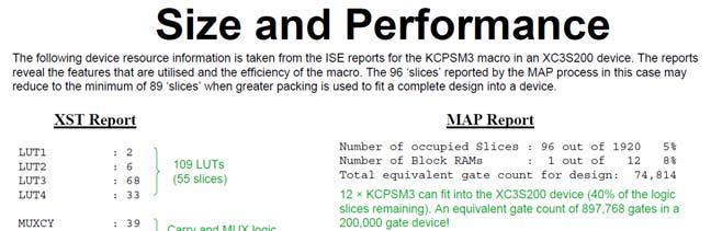
 PicoBlaze 8-bit Embedded Microcontroller 1 PicoBlaze Overview PicoBlaze is a simple 8-bit microcontroller Compact in size Occupies 96 slices in a Spartan-3 (5% of an XC3S200) Performance is respectable
EITF35: Introduction to Structured VLSI Design
 EITF35: Introduction to Structured VLSI Design Introduction to FPGA design Rakesh Gangarajaiah Rakesh.gangarajaiah@eit.lth.se Slides from Chenxin Zhang and Steffan Malkowsky WWW.FPGA What is FPGA? Field
Agenda. PicoBlaze Hello World project using the PicoBlaze. Class 9 Copyright 2011 Greg Tumbush Ver 1.0 1
 Agenda PicoBlaze Hello World project using the PicoBlaze Class 9 Copyright 2011 Greg Tumbush Ver 1.0 1 Embedded Processor Why? Firmware is easier to maintain/modify/deploy If the constraints of you system
The Xilinx XC6200 chip, the software tools and the board development tools
 The Xilinx XC6200 chip, the software tools and the board development tools What is an FPGA? Field Programmable Gate Array Fully programmable alternative to a customized chip Used to implement functions
FIELD PROGRAMMABLE GATE ARRAYS (FPGAS)
") FIELD PROGRAMMABLE GATE ARRAYS (FPGAS) 1 Roth Text: Chapter 3 (section 3.4) Chapter 6 Nelson Text: Chapter 11 Programmable logic taxonomy Lab Device 2 Field Programmable Gate Arrays Typical Complexity
FIELD PROGRAMMABLE GATE ARRAYS (FPGAS) 1 Roth Text: Chapter 3 (section 3.4) Chapter 6 Nelson Text: Chapter 11 Programmable logic taxonomy Lab Device 2 Field Programmable Gate Arrays Typical Complexity
Implementing a PicoBlaze microprocessor structure (state machine) using a reconfigurable hardware medium
 using a reconfigurable hardware medium") Laboratory number 3 Implementing a PicoBlaze microprocessor structure (state machine) using a reconfigurable hardware medium Purpose of the laboratory: A PicoBlaze TM processor version for Virtex, Virtex-E,
Laboratory number 3 Implementing a PicoBlaze microprocessor structure (state machine) using a reconfigurable hardware medium Purpose of the laboratory: A PicoBlaze TM processor version for Virtex, Virtex-E,
EECS150 - Digital Design Lecture 6 - Field Programmable Gate Arrays (FPGAs)
") EECS150 - Digital Design Lecture 6 - Field Programmable Gate Arrays (FPGAs) September 12, 2002 John Wawrzynek Fall 2002 EECS150 - Lec06-FPGA Page 1 Outline What are FPGAs? Why use FPGAs (a short history
EECS150 - Digital Design Lecture 6 - Field Programmable Gate Arrays (FPGAs) September 12, 2002 John Wawrzynek Fall 2002 EECS150 - Lec06-FPGA Page 1 Outline What are FPGAs? Why use FPGAs (a short history
Outline. EECS150 - Digital Design Lecture 6 - Field Programmable Gate Arrays (FPGAs) FPGA Overview. Why FPGAs?
 FPGA Overview. Why FPGAs?") EECS150 - Digital Design Lecture 6 - Field Programmable Gate Arrays (FPGAs) September 12, 2002 John Wawrzynek Outline What are FPGAs? Why use FPGAs (a short history lesson). FPGA variations Internal logic
EECS150 - Digital Design Lecture 6 - Field Programmable Gate Arrays (FPGAs) September 12, 2002 John Wawrzynek Outline What are FPGAs? Why use FPGAs (a short history lesson). FPGA variations Internal logic
INTRODUCTION TO FIELD PROGRAMMABLE GATE ARRAYS (FPGAS)
") INTRODUCTION TO FIELD PROGRAMMABLE GATE ARRAYS (FPGAS) Bill Jason P. Tomas Dept. of Electrical and Computer Engineering University of Nevada Las Vegas FIELD PROGRAMMABLE ARRAYS Dominant digital design
INTRODUCTION TO FIELD PROGRAMMABLE GATE ARRAYS (FPGAS) Bill Jason P. Tomas Dept. of Electrical and Computer Engineering University of Nevada Las Vegas FIELD PROGRAMMABLE ARRAYS Dominant digital design
The QR code here provides a shortcut to go to the course webpage.
 Welcome to this MSc Lab Experiment. All my teaching materials for this Lab-based module are also available on the webpage: www.ee.ic.ac.uk/pcheung/teaching/msc_experiment/ The QR code here provides a shortcut
EE 109 Unit 12 Computer Organization
 1 EE 19 Unit 12 Computer Organization 2 Review of some key concepts from the first half of the semester A BRIEF SUMMARY 3 A Few Big Ideas 1 Setting and clearing bits in a register tells the hardware what
Programmable Logic Devices FPGA Architectures II CMPE 415. Overview This set of notes introduces many of the features available in the FPGAs of today.
 Overview This set of notes introduces many of the features available in the FPGAs of today. The majority use SRAM based configuration cells, which allows fast reconfiguation. Allows new design ideas to
FPGA Based Digital Design Using Verilog HDL
 FPGA Based Digital Design Using Course Designed by: IRFAN FAISAL MIR ( Verilog / FPGA Designer ) irfanfaisalmir@yahoo.com * Organized by Electronics Division Integrated Circuits Uses for digital IC technology
What is Xilinx Design Language?
 Bill Jason P. Tomas University of Nevada Las Vegas Dept. of Electrical and Computer Engineering What is Xilinx Design Language? XDL is a human readable ASCII format compatible with the more widely used
Outcomes. Spiral 1 / Unit 6. Flip Flops FLIP FLOPS AND REGISTERS. Flip flops and Registers. Outputs only change once per clock period
 1-6.1 1-6.2 Spiral 1 / Unit 6 Flip flops and Registers Mark Redekopp Outcomes I know the difference between combinational and sequential logic and can name examples of each. I understand latency, throughput,
A Study of the Speedups and Competitiveness of FPGA Soft Processor Cores using Dynamic Hardware/Software Partitioning
 A Study of the Speedups and Competitiveness of FPGA Soft Processor Cores using Dynamic Hardware/Software Partitioning By: Roman Lysecky and Frank Vahid Presented By: Anton Kiriwas Disclaimer This specific
FPGA: What? Why? Marco D. Santambrogio
 FPGA: What? Why? Marco D. Santambrogio marco.santambrogio@polimi.it 2 Reconfigurable Hardware Reconfigurable computing is intended to fill the gap between hardware and software, achieving potentially much
Topics. Midterm Finish Chapter 7
 Lecture 9 Topics Midterm Finish Chapter 7 Xilinx FPGAs Chapter 7 Spartan 3E Architecture Source: Spartan-3E FPGA Family Datasheet CLB Configurable Logic Blocks Each CLB contains four slices Each slice
Outcomes. Spiral 1 / Unit 6. Flip Flops FLIP FLOPS AND REGISTERS. Flip flops and Registers. Outputs only change once per clock period
 1-5.1 1-5.2 Spiral 1 / Unit 6 Flip flops and Registers Mark Redekopp Outcomes I know the difference between combinational and sequential logic and can name examples of each. I understand latency, throughput,
L2: FPGA HARDWARE : ADVANCED DIGITAL DESIGN PROJECT FALL 2015 BRANDON LUCIA
 L2: FPGA HARDWARE 18-545: ADVANCED DIGITAL DESIGN PROJECT FALL 2015 BRANDON LUCIA 18-545: FALL 2014 2 Admin stuff Project Proposals happen on Monday Be prepared to give an in-class presentation Lab 1 is
PicoBlaze Instruction Set and Event Reference
 Appendix C PicoBlaze Instruction Set and Event Reference This appendix provides a detailed operational description of each PicoBlaze instruction and the Interrupt and Reset events, including pseudocode
EE 109 Unit 12 Computer Organization. A Few Big Ideas 1. A Few Big Ideas 2 A BRIEF SUMMARY. Clocking or enables are necessary to say
 EE 9 Unit Computer Organization Review of some key concepts from the first half of the semester and revisit what CECS prepares you to do in the future. A BRIEF SUMMARY A Few Big Ideas bits in a register
discrete logic do not
 Welcome to my second year course on Digital Electronics. You will find that the slides are supported by notes embedded with the Powerpoint presentations. All my teaching materials are also available on
System-on Solution from Altera and Xilinx
 System-on on-a-programmable-chip Solution from Altera and Xilinx Xun Yang VLSI CAD Lab, Computer Science Department, UCLA FPGAs with Embedded Microprocessors Combination of embedded processors and programmable
ECEN 449 Microprocessor System Design. FPGAs and Reconfigurable Computing
 ECEN 449 Microprocessor System Design FPGAs and Reconfigurable Computing Some of the notes for this course were developed using the course notes for ECE 412 from the University of Illinois, Urbana-Champaign
Overview. CSE372 Digital Systems Organization and Design Lab. Hardware CAD. Two Types of Chips
 Overview CSE372 Digital Systems Organization and Design Lab Prof. Milo Martin Unit 5: Hardware Synthesis CAD (Computer Aided Design) Use computers to design computers Virtuous cycle Architectural-level,
Workspace for '4-FPGA' Page 1 (row 1, column 1)
") Workspace for '4-FPGA' Page 1 (row 1, column 1) Workspace for '4-FPGA' Page 2 (row 2, column 1) Workspace for '4-FPGA' Page 3 (row 3, column 1) ECEN 449 Microprocessor System Design FPGAs and Reconfigurable
Workspace for '4-FPGA' Page 1 (row 1, column 1) Workspace for '4-FPGA' Page 2 (row 2, column 1) Workspace for '4-FPGA' Page 3 (row 3, column 1) ECEN 449 Microprocessor System Design FPGAs and Reconfigurable
Spiral 1 / Unit 6. Flip-flops and Registers
 1-5.1 Spiral 1 / Unit 6 Flip-flops and Registers 1-5.2 Outcomes I know the difference between combinational and sequential logic and can name examples of each. I understand latency, throughput, and at
Today. Comments about assignment Max 1/T (skew = 0) Max clock skew? Comments about assignment 3 ASICs and Programmable logic Others courses
 Max clock skew? Comments about assignment 3 ASICs and Programmable logic Others courses") Today Comments about assignment 3-43 Comments about assignment 3 ASICs and Programmable logic Others courses octor Per should show up in the end of the lecture Mealy machines can not be coded in a single
Today Comments about assignment 3-43 Comments about assignment 3 ASICs and Programmable logic Others courses octor Per should show up in the end of the lecture Mealy machines can not be coded in a single
ECE 448 Lecture 5. FPGA Devices
 ECE 448 Lecture 5 FPGA Devices George Mason University Required reading Spartan-6 FPGA Configurable Logic Block: User Guide CLB Overview Slice Description 2 Recommended reading Highly recommended for the
DSP Co-Processing in FPGAs: Embedding High-Performance, Low-Cost DSP Functions
 White Paper: Spartan-3 FPGAs WP212 (v1.0) March 18, 2004 DSP Co-Processing in FPGAs: Embedding High-Performance, Low-Cost DSP Functions By: Steve Zack, Signal Processing Engineer Suhel Dhanani, Senior
Hardware Design with VHDL PLDs IV ECE 443
 Embedded Processor Cores (Hard and Soft) Electronic design can be realized in hardware (logic gates/registers) or software (instructions executed on a microprocessor). The trade-off is determined by how
Computer Systems. Binary Representation. Binary Representation. Logical Computation: Boolean Algebra
 Binary Representation Computer Systems Information is represented as a sequence of binary digits: Bits What the actual bits represent depends on the context: Seminar 3 Numerical value (integer, floating
Spiral 1 / Unit 4 Verilog HDL. Digital Circuit Design Steps. Digital Circuit Design OVERVIEW. Mark Redekopp. Description. Verification.
 1-4.1 1-4.2 Spiral 1 / Unit 4 Verilog HDL Mark Redekopp OVERVIEW 1-4.3 1-4.4 Digital Circuit Design Steps Digital Circuit Design Description Design and computer-entry of circuit Verification Input Stimulus
The Nios II Family of Configurable Soft-core Processors
 The Nios II Family of Configurable Soft-core Processors James Ball August 16, 2005 2005 Altera Corporation Agenda Nios II Introduction Configuring your CPU FPGA vs. ASIC CPU Design Instruction Set Architecture
Getting to Work with OpenPiton. Princeton University. OpenPit
 Getting to Work with OpenPiton Princeton University http://openpiton.org OpenPit Princeton Parallel Research Group Redesigning the Data Center of the Future Chip Architecture Operating Systems and Runtimes
Hardware Design Environments. Dr. Mahdi Abbasi Computer Engineering Department Bu-Ali Sina University
 Hardware Design Environments Dr. Mahdi Abbasi Computer Engineering Department Bu-Ali Sina University Outline Welcome to COE 405 Digital System Design Design Domains and Levels of Abstractions Synthesis
FPGA architecture and design technology
 CE 435 Embedded Systems Spring 2017 FPGA architecture and design technology Nikos Bellas Computer and Communications Engineering Department University of Thessaly 1 FPGA fabric A generic island-style FPGA
PROGRAMMABLE MODULES SPECIFICATION OF PROGRAMMABLE COMBINATIONAL AND SEQUENTIAL MODULES
 PROGRAMMABLE MODULES SPECIFICATION OF PROGRAMMABLE COMBINATIONAL AND SEQUENTIAL MODULES. psa. rom. fpga THE WAY THE MODULES ARE PROGRAMMED NETWORKS OF PROGRAMMABLE MODULES EXAMPLES OF USES Programmable
Nexys 2/3 board tutorial (Decoder, ISE 13.2) Jim Duckworth, August 2011, WPI. (updated March 2012 to include Nexys2 board)
 Jim Duckworth, August 2011, WPI. (updated March 2012 to include Nexys2 board)") Nexys 2/3 board tutorial (Decoder, ISE 13.2) Jim Duckworth, August 2011, WPI. (updated March 2012 to include Nexys2 board) Note: you will need the Xilinx ISE Webpack installed on your computer (or you
Nexys 2/3 board tutorial (Decoder, ISE 13.2) Jim Duckworth, August 2011, WPI. (updated March 2012 to include Nexys2 board) Note: you will need the Xilinx ISE Webpack installed on your computer (or you
Verilog Simulation Mapping
 1 Motivation UNIVERSITY OF CALIFORNIA AT BERKELEY COLLEGE OF ENGINEERING DEPARTMENT OF ELECTRICAL ENGINEERING AND COMPUTER SCIENCE Lab 4 Verilog Simulation Mapping In this lab you will learn how to use
FPGA Implementations
 FPGA Implementations Smith Text: Chapters 4-8 Online version at: http://www10.edacafe.com/book/asic/asics.php Topic outline Chapter 4 Programmable ASIC technologies Chapter 5 Programmable logic cells Chapter
Lab 4: Register File and Memory 50 points Instructor: Yifeng Zhu Due: One week
 Objectives: Lab 4: Register File and Memory 50 points Instructor: Yifeng Zhu Due: One week Build Register File Build Instruction Memory and Data Memory 1. Overview A combinational circuit neither contains
Reading Spartan-3A Device DNA
 Reading Spartan-3A Device DNA A Reference Design for the Spartan-3A Starter Kit Includes an LCD display driver Rev2 10 th July 2007 Ken Chapman Xilinx Ltd Limitations Limited Warranty and Disclaimer. These
ECE 313 Computer Organization EXAM 2 November 11, 2000
 This exam is open book and open notes. You have 50 minutes. Credit for problems requiring calculation will be given only if you show your work. 1. ALU Design / Logic Operations 20 Points The subset of
Digital Systems Laboratory
 2012 Fall CSE140L Digital Systems Laboratory by Dr. Choon Kim CSE Department UCSD 1 Welcome to CSE140L! 2 3-way Light Controller, 2-1 MUX, Majority Detector, 7- seg Display, Binary-to- Decimal converter.
MIGRATING MICROCONTROLLER BASED CONTROL SYSTEMS INTO THE NANO FABRICS OF FPGAS
 MIGRATING MICROCONTROLLER BASED CONTROL SYSTEMS INTO THE NANO FABRICS OF FPGAS Santosh A. Shinde, Vinod G. Shelake and R. K. Kamat* VLSI Laboratory, Department of Electronics, Shivaji University, KOLHAPUR
Topics. Midterm Finish Chapter 7
 Lecture 9 Topics Midterm Finish Chapter 7 ROM (review) Memory device in which permanent binary information is stored. Example: 32 x 8 ROM Five input lines (2 5 = 32) 32 outputs, each representing a memory
CS 31: Intro to Systems Digital Logic. Kevin Webb Swarthmore College February 2, 2016
 CS 31: Intro to Systems Digital Logic Kevin Webb Swarthmore College February 2, 2016 Reading Quiz Today Hardware basics Machine memory models Digital signals Logic gates Circuits: Borrow some paper if
EECS 150 Homework 7 Solutions Fall (a) 4.3 The functions for the 7 segment display decoder given in Section 4.3 are:
 4.3 The functions for the 7 segment display decoder given in Section 4.3 are:") Problem 1: CLD2 Problems. (a) 4.3 The functions for the 7 segment display decoder given in Section 4.3 are: C 0 = A + BD + C + BD C 1 = A + CD + CD + B C 2 = A + B + C + D C 3 = BD + CD + BCD + BC C 4
Problem 1: CLD2 Problems. (a) 4.3 The functions for the 7 segment display decoder given in Section 4.3 are: C 0 = A + BD + C + BD C 1 = A + CD + CD + B C 2 = A + B + C + D C 3 = BD + CD + BCD + BC C 4
ECE 437 Computer Architecture and Organization Lab 6: Programming RAM and ROM Due: Thursday, November 3
 Objectives: ECE 437 Computer Architecture and Organization Lab 6: Programming RAM and ROM Due: Thursday, November 3 Build Instruction Memory and Data Memory What to hand in: Your implementation source
Design and Implementation of an AHB SRAM Memory Controller
 Design and Implementation of an AHB SRAM Memory Controller 1 Module Overview Learn the basics of Computer Memory; Design and implement an AHB SRAM memory controller, which replaces the previous on-chip
ALTERA FPGAs Architecture & Design
 ALTERA FPGAs Architecture & Design Course Description This course provides all theoretical and practical know-how to design programmable devices of ALTERA with QUARTUS-II design software. The course combines
Lab 1: FPGA Physical Layout
 Lab 1: FPGA Physical Layout University of California, Berkeley Department of Electrical Engineering and Computer Sciences EECS150 Components and Design Techniques for Digital Systems John Wawrzynek, James
The DSP Primer 8. FPGA Technology. DSPprimer Home. DSPprimer Notes. August 2005, University of Strathclyde, Scotland, UK
 The DSP Primer 8 FPGA Technology Return DSPprimer Home Return DSPprimer Notes August 2005, University of Strathclyde, Scotland, UK For Academic Use Only THIS SLIDE IS BLANK August 2005, For Academic Use
EE260: Digital Design, Spring 2018
 Topics Verilog Module 1 Introduction Yao Zheng (Based on the slides of Prof. Jim Duckworth) Background to Verilog Introduction to language Programmable Logic Devices CPLDs and FPGAs FPGA architecture Nexys
The Next Generation 65-nm FPGA. Steve Douglass, Kees Vissers, Peter Alfke Xilinx August 21, 2006
 The Next Generation 65-nm FPGA Steve Douglass, Kees Vissers, Peter Alfke Xilinx August 21, 2006 Hot Chips, 2006 Structure of the talk 65nm technology going towards 32nm Virtex-5 family Improved I/O Benchmarking
Advanced FPGA Design Methodologies with Xilinx Vivado
 Advanced FPGA Design Methodologies with Xilinx Vivado Lecturer: Alexander Jäger Course of studies: Technische Informatik Student number: 3158849 Date: 30.01.2015 30/01/15 Advanced FPGA Design Methodologies
SP3Q.3. What makes it a good idea to put CRC computation and error-correcting code computation into custom hardware?
 Part II CST: SoC D/M: Quick exercises S3-S4 (examples sheet) Feb 2018 (rev a). This sheet contains short exercises for quick revision. Please also look at past exam questions and/or try some of the longer
Basic FPGA Architectures. Actel FPGAs. PLD Technologies: Antifuse. 3 Digital Systems Implementation Programmable Logic Devices
 3 Digital Systems Implementation Programmable Logic Devices Basic FPGA Architectures Why Programmable Logic Devices (PLDs)? Low cost, low risk way of implementing digital circuits as application specific
Introduction to FPGAs. H. Krüger Bonn University
 Introduction to FPGAs H. Krüger Bonn University Outline 1. History 2. FPGA Architecture 3. Current Trends 4. Design Methodology (short see other lectures) Disclaimer: Most of the resources used for this
COSC 122 Computer Fluency. Computer Organization. Dr. Ramon Lawrence University of British Columbia Okanagan
 COSC 122 Computer Fluency Computer Organization Dr. Ramon Lawrence University of British Columbia Okanagan ramon.lawrence@ubc.ca Key Points 1) The standard computer (von Neumann) architecture consists
EE 1315 DIGITAL LOGIC LAB EE Dept, UMD
 EE 1315 DIGITAL LOGIC LAB EE Dept, UMD EXPERIMENT # 1: Logic building blocks The main objective of this experiment is to let you familiarize with the lab equipment and learn about the operation of the
Lecture 7: Introduction to Co-synthesis Algorithms
 Design & Co-design of Embedded Systems Lecture 7: Introduction to Co-synthesis Algorithms Sharif University of Technology Computer Engineering Dept. Winter-Spring 2008 Mehdi Modarressi Topics for today
University of Hawaii EE 361L. Getting Started with Spartan 3E Digilent Basys2 Board. Lab 4.1
 University of Hawaii EE 361L Getting Started with Spartan 3E Digilent Basys2 Board Lab 4.1 I. Test Basys2 Board Attach the Basys2 board to the PC or laptop with the USB connector. Make sure the blue jumper
Microcomputer Architecture and Programming
 IUST-EE (Chapter 1) Microcomputer Architecture and Programming 1 Outline Basic Blocks of Microcomputer Typical Microcomputer Architecture The Single-Chip Microprocessor Microprocessor vs. Microcontroller
Overview of SOC Architecture design
 Computer Architectures Overview of SOC Architecture design Tien-Fu Chen National Chung Cheng Univ. SOC - 0 SOC design Issues SOC architecture Reconfigurable System-level Programmable processors Low-level
COE 561 Digital System Design & Synthesis Introduction
 1 COE 561 Digital System Design & Synthesis Introduction Dr. Aiman H. El-Maleh Computer Engineering Department King Fahd University of Petroleum & Minerals Outline Course Topics Microelectronics Design
A Brief Introduction to Verilog Hardware Definition Language (HDL)
") www.realdigital.org A Brief Introduction to Verilog Hardware Definition Language (HDL) Forward Verilog is a Hardware Description language (HDL) that is used to define the structure and/or behavior of digital
www.realdigital.org A Brief Introduction to Verilog Hardware Definition Language (HDL) Forward Verilog is a Hardware Description language (HDL) that is used to define the structure and/or behavior of digital
V8-uRISC 8-bit RISC Microprocessor AllianceCORE Facts Core Specifics VAutomation, Inc. Supported Devices/Resources Remaining I/O CLBs
 V8-uRISC 8-bit RISC Microprocessor February 8, 1998 Product Specification VAutomation, Inc. 20 Trafalgar Square Nashua, NH 03063 Phone: +1 603-882-2282 Fax: +1 603-882-1587 E-mail: sales@vautomation.com
EE 459/500 HDL Based Digital Design with Programmable Logic
 EE 459/500 HDL Based Digital Design with Programmable Logic Lecture 17 From special-purpose FSMD to general-purpose microcontroller: Xilinx s PicoBlaze 1 Overview From FSMD to Microcontroller PicoBlaze
PICOBLAZE INTERRUPT INTERFACE
 CHAPTER 17 PICOBLAZE INTERRUPT INTERFACE 17.1 INTRODUCTION During normal program execution, a microcontroller polls the I/O peripherals (i.e., checks the status signals) and determines the course of action
Advanced FPGA Design Methodologies with Xilinx Vivado
 Advanced FPGA Design Methodologies with Xilinx Vivado Alexander Jäger Computer Architecture Group Heidelberg University, Germany Abstract With shrinking feature sizes in the ASIC manufacturing technology,
More Course Information
 More Course Information Labs and lectures are both important Labs: cover more on hands-on design/tool/flow issues Lectures: important in terms of basic concepts and fundamentals Do well in labs Do well
CSE 141L Computer Architecture Lab Fall Lecture 3
 CSE 141L Computer Architecture Lab Fall 2005 Lecture 3 Pramod V. Argade November 1, 2005 Fall 2005 CSE 141L Course Schedule Lecture # Date Day Lecture Topic Lab Due 1 9/27 Tuesday No Class 2 10/4 Tuesday
Keywords: Soft Core Processor, Arithmetic and Logical Unit, Back End Implementation and Front End Implementation.
 ISSN 2319-8885 Vol.03,Issue.32 October-2014, Pages:6436-6440 www.ijsetr.com Design and Modeling of Arithmetic and Logical Unit with the Platform of VLSI N. AMRUTHA BINDU 1, M. SAILAJA 2 1 Dept of ECE,
Chapter 1 Overview of Digital Systems Design
 Chapter 1 Overview of Digital Systems Design SKEE2263 Digital Systems Mun im/ismahani/izam {munim@utm.my,e-izam@utm.my,ismahani@fke.utm.my} February 8, 2017 Why Digital Design? Many times, microcontrollers
Block Diagram. mast_sel. mast_inst. mast_data. mast_val mast_rdy. clk. slv_sel. slv_inst. slv_data. slv_val slv_rdy. rfifo_depth_log2.
 Key Design Features Block Diagram Synthesizable, technology independent IP Core for FPGA, ASIC and SoC reset Supplied as human readable VHDL (or Verilog) source code mast_sel SPI serial-bus compliant Supports
ESE532: System-on-a-Chip Architecture. Today. Message. Graph Cycles. Preclass 1. Reminder
 ESE532: System-on-a-Chip Architecture Day 8: September 26, 2018 Spatial Computations Today Graph Cycles (from Day 7) Accelerator Pipelines FPGAs Zynq Computational Capacity 1 2 Message Custom accelerators
Lecture 41: Introduction to Reconfigurable Computing
 inst.eecs.berkeley.edu/~cs61c CS61C : Machine Structures Lecture 41: Introduction to Reconfigurable Computing Michael Le, Sp07 Head TA April 30, 2007 Slides Courtesy of Hayden So, Sp06 CS61c Head TA Following
FPGA How do they work?
 ent FPGA How do they work? ETI135, Advanced Digital IC Design What is a FPGA? Manufacturers Distributed RAM History FPGA vs ASIC FPGA and Microprocessors Alternatives to FPGAs Anders Skoog, Stefan Granlund