High Capacity and High Performance 20nm FPGAs. Steve Young, Dinesh Gaitonde August Copyright 2014 Xilinx
|
|
|
- Logan Kennedy
- 6 years ago
- Views:
Transcription


1 High Capacity and High Performance 20nm FPGAs Steve Young, Dinesh Gaitonde August 2014


2 Not a Complete Product Overview Page 2


3 Outline Page 3


4 Petabytes per month Increasing Bandwidth Global IP Traffic Growth Growth of Xilinx FPGA Serial Bandwidth 6 Tb/s 5 Tb/s 4 Tb/s 3 Tb/s 2 Tb/s 1 Tb/s 1: Cisco Visual Networking Index, Forecast and Methodology, nm 90nm 65nm 40nm 28nm 20nm N Page 4


5 Higher Bandwidth IO Page 5
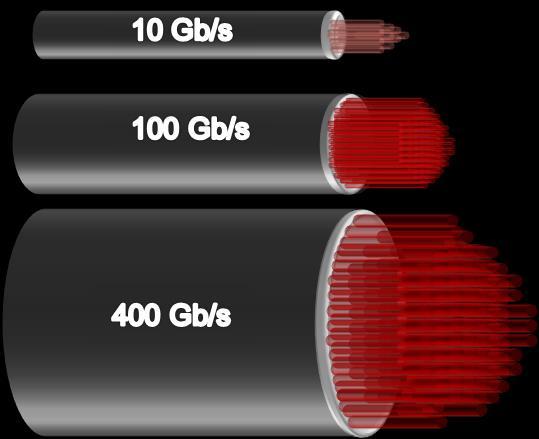
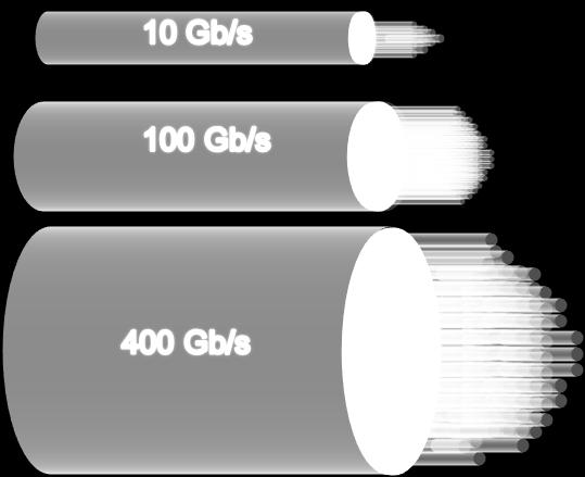


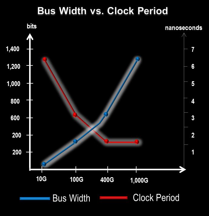


6 High Throughput Demands Wider, Faster Data Paths 1,000 Gb/s Page 6
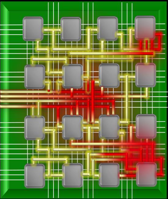
7 Addressing Interconnect Bottlenecks Page 7


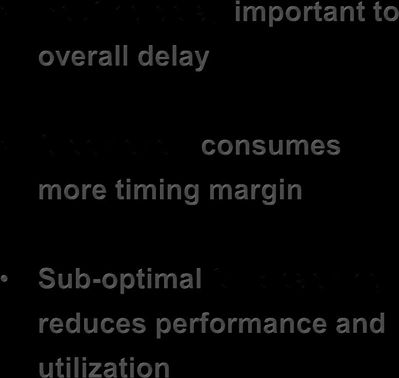
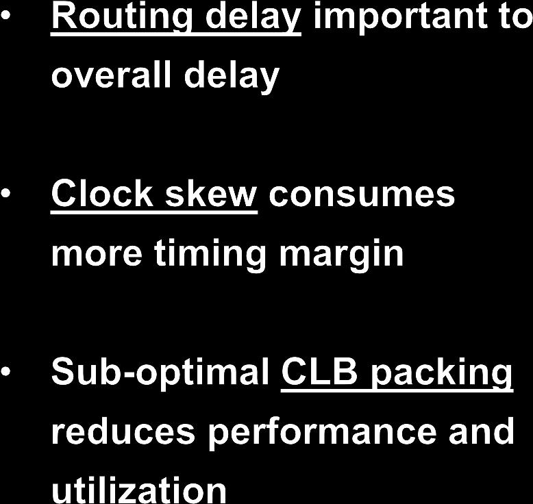
8 Clocking Challenge Page 8


9 Benefits of UltraScale Clock Architecture Clock Domain 1 Clock Domain 1 32 Clock Domain 2 Clock Domain 2 Clock Domain 3 Global Clock Network Leaf Cell Clocks Clocking 32 centrally located global clock buffers Root always in center of device I/O Logic GT Clock Root Distribution Clocks Routing Clocks distributed global buffers Root can be in any clock region Skew accumulates from center to edge Balanced skew per clock network Page 9

10 Routing Challenge Page 10


11 CLB Innovations Enable Tighter Packing Removed slice boundary & added MUX Wider functions per block 2x distributed RAM density Wider carry chain Wider functions per block CLB = Slice Slice 0 UltraScale 7 Series CLB carry out Flip-flops sharing same CE are same color Dedicated inputs for each flip-flop Higher performance Reduces LUT utilization UltraScale 7 Series LUT U independent direct route Slice 1 U carry in carry out Bypass CE ignore and RST ignore, RST inversion Higher performance Eliminates synchronous reset bottlenecks 2x the number of CE s Improves CLB packing RST ignore, inversion CE ignore D IN RST CE Flip-flops sharing same CE are same color carry in Page 11


12 Total Wire Length Design Use Fewer CLBs, Shorter Wire Length Re-architected for flexible connectivity and efficient logic packing Better local routability, more control set flexibility, improved P&R algorithms Tighter packing results in shorter net delays, less wire switching Translates into higher utilization, greater performance, less power Total Wirelength UltraScale & Vivado vs Previous Architecture (Normalized to 7 series) 10 Average 7 series UltraScale Fully Used CLB Partially Used CLB Individual Designs Page 12

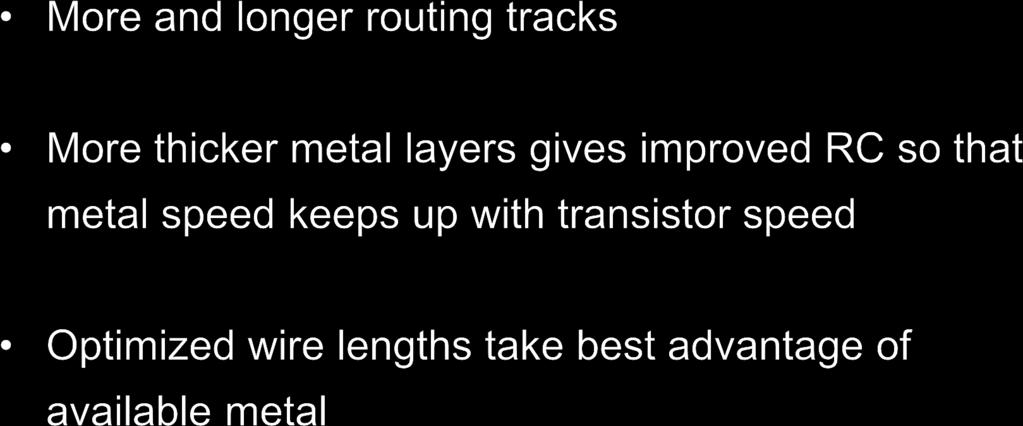
13 Additional Metal Layers Page 13
14 Routing complexity Routability Benchmark Suite Metrics: Design Routing Complexity and Design Size Congestion Metrics displayed in Vivado No routing congestion High routing congestion Cannot route No congestion Design Size Page 14

15 Routing complexity Routing complexity UltraScale Results Vivado routes more complex designs on UltraScale UltraScale shows lower congestion on complex designs As a result, timing closure is accelerated Delivers 1 speedgrade higher Fmax No routing congestion High routing congestion Cannot route Page 15


16 2nd Generation Stacked Silicon Feature ~20,000 registered routing lines between die Clocking Architecture Spans SLR boundaries Foot-print compatibility between SSI and non-ssi devices Benefit Enables >500 MHz datapath performance between SLRs Deterministic, predictable timing Device size up to 44 million logic cells Abundant clock resources to meet demanding application Ability to seamlessly migrate from monolithic to 3D-IC devices SLR0 SLR1 SLR2 passive interposer Substrate Page 16


 up to 30% up to")
 BRAM hardened data cascading BRAM dynamic")

17 Power Optimizations Transceiver I/O up to 60% up to 50% Architectural optimizations Low power mode I/O multi-mode control (cont d from 28nm) DDR4 voltage reduction Dynamic up to 30% CLB packing & reduced wire length HW based clock gating on leaf cells Static Spartan-6/Virtex-6 (45nm/40nm) up to 50% up to 65% Transceiver I/O Dynamic Static 7 Series (28nm) up to 30% up to 40% up to 50% up to 40% 25-45% Transceiver I/O Dynamic Static UltraScale (20nm/16nm) BRAM hardened data cascading BRAM dynamic power gating DSP hardened features MMCM & PLL lower supply voltage Process node Power binning & lower voltage scaling 3D IC static power binned slices Page 17
18 Kintex UltraScale FPGAs Logic Resources Memory Resources Clock Resources I/O Resources Integrated IP Resources Speed Grades Footprint Compatible with Virtex UltraScale Page 18 Part Number XCKU035 XCKU040 XCKU060 XCKU075 XCKU100 XCKU115 Logic Cells 355, , , , ,440 1,160,880 CLB Flip-Flops 406, , , ,000 1,095,360 1,326,720 CLB LUTs 203, , , , , ,360 Maximum Distributed RAM (Kb) 5,908 7,050 9,180 7,290 12,825 18,360 Block RAM/FIFO w/ecc (36 Kb each) ,080 1,188 1,680 2,160 Block RAM/FIFO (18 Kb each) 1,080 1,200 2,160 2,376 3,360 4,320 Total Block RAM (Mb) CMT (1 MMCM, 2 PLLs) I/O DLL Maximum Single-Ended HP I/Os Maximum Differential HP I/O Pairs Maximum Single-Ended HR I/Os Maximum Differential HR I/O Pairs DSP Slices 1,700 1,920 2,760 2,592 4,200 5,520 System Monitor PCIe Gen1/2/ Interlaken G Ethernet GTH 16 Gb/s Transceivers Commercial Extended Industrial -1-1L L L L L L -2 Package Package Footprint Dimensions (mm) HR I/O, HP I/O, GTH 16 Gb/s A676 27x27 104, 208, , 208, 16 A900 31x31 104, 364, , 364, 16 A x35 104, 416, , 416, , 416, , 416, 28 A x40 104, 520, , 520, , 520, , 520, 48 B x40 104, 260, , 260, 64 A , 624, x425 A , 624, , 624, 52 D x45 156, 676, , 676, 52 F x45 104, 624, , 624, 64
19 Virtex UltraScale FPGAs Memory Resources Clock Resources I/O Resources Integrated IP Resources Speed Grades Footprint Compatible with Kintex UltraScale Devices Page 19 Part Number XCVU065 XCVU080 XCVU095 XCVU125 XCVU160 XCVU190 XCVU440 Logic Cells 626, , ,800 1,253,280 1,621,200 1,879,920 4,407,480 CLB Flip-Flops 716, ,424 1,075,200 1,432,320 1,852,800 2,148,480 5,037,120 CLB LUTs 358, , , , ,400 1,074,240 2,518,560 Maximum Distributed RAM (Kb) 4,230 3,980 4,800 8,460 10,710 12,690 28,710 Block RAM/FIFO w/ecc (36 Kb each) 1,260 1,421 1,728 2,520 3,276 3,780 2,520 Block RAM/FIFO (18 Kb each) 2,520 2,842 3,456 5,040 6,552 7,560 5,040 Total Block RAM (Mb) CMT (1 MMCM, 2 PLLs) I/O DLL Fractional PLL Maximum Single-Ended HP I/Os ,404 Maximum Differential HP I/O Pairs Maximum Single-Ended HR I/Os Maximum Differential HR I/O Pairs DSP Slices ,200 1,560 1,800 2,880 System Monitor PCIe Gen1/2/ Interlaken G Ethernet GTH 16 Gb/s Transceivers GTY 33 Gb/s Transceivers Commercial Extended Industrial -1-1L L L L L L L -2 Package Package Footprint (1) Dimensions (mm) HR I/O, HP I/O, GTH 16 Gb/s, GTY 33 Gb/s C x40 52, 468, 20, 20 52, 468, 24, 24 52, 468, 24, 24 B x40 52, 312, 32, 32 52, 312, 32, 32 52, 312, 40, 32 A x425 52, 676, 32, 16 52, 676, 32, 16 52, 676, 36, 16 D x45 52, 780, 28, 24 52, 780, 28, 24 52, 780, 28, 24 E x45 52, 624, 32, 32 52, 624, 32, 32 52, 624, 36, x475 (2) 52, 624, 36, 36 52, 624, 36, 36 J x45 52, 312, 32, 32 52, 312, 40, x475 (2) 52, 312, 52, 52 52, 312, 52, 52 A x50 104, 936, 28, 24 52, 988, 28, 24 52, 988, 28, 24 B x50 52, 1248, 36, 0 C x50 0, 520, 60, 60 A x55 52, 1404, 48, 0
20 Key Takeaways Increased IO bandwidth Up to 120 transceivers Up to 33 Gb/s per channel Routing architecture and Vivado designed to reduce congestion and improve performance Clocking architecture for flexibility and performance 2 nd generation SSI delivers "more than Moore" Up to 44 million logic cells in largest device Breakthrough architecture to address the most complex designs

21 Thank You! Page 21
Copyright 2017 Xilinx.
 All Programmable Automotive SoC Comparison XA Zynq UltraScale+ MPSoC ZU2/3EG, ZU4/5EV Devices XA Zynq -7000 SoC Z-7010/7020/7030 Devices Application Processor Real-Time Processor Quad-core ARM Cortex -A53
UltraScale Architecture and Product Overview
 UltraScale Architecture and Product Overview Product Specification General Description Xilinx UltraScale architecture comprises two high-performance FPGA families that address a vast spectrum of system
Zynq AP SoC Family
 Programmable Logic (PL) Processing System (PS) Zynq -7000 AP SoC Family Cost-Optimized Devices Mid-Range Devices Device Name Z-7007S Z-7012S Z-7014S Z-7010 Z-7015 Z-7020 Z-7030 Z-7035 Z-7045 Z-7100 Part
UltraScale Architecture: Highest Device Utilization, Performance, and Scalability
 White Paper: UltraScale FPGAs WP455 (v1.2) October 29, 2015 UltraScale Architecture: Highest Device Utilization, Performance, and Scalability By: Nick Mehta High-performance architecture and extensive
Reconfigurable Computing
 Reconfigurable Computing FPGA Architecture Architecture should speak of its time and place, but yearn for timelessness. Frank Gehry Philip Leong (philip.leong@sydney.edu.au) School of Electrical and Information
High Performance Memory in FPGAs
 High Performance Memory in FPGAs Industry Trends and Customer Challenges Packet Processing & Transport > 400G OTN Software Defined Networks Video Over IP Network Function Virtualization Wireless LTE Advanced
Zynq-7000 All Programmable SoC Product Overview
 Zynq-7000 All Programmable SoC Product Overview The SW, HW and IO Programmable Platform August 2012 Copyright 2012 2009 Xilinx Introducing the Zynq -7000 All Programmable SoC Breakthrough Processing Platform
FPGA architecture and design technology
 CE 435 Embedded Systems Spring 2017 FPGA architecture and design technology Nikos Bellas Computer and Communications Engineering Department University of Thessaly 1 FPGA fabric A generic island-style FPGA
CPE/EE 422/522. Introduction to Xilinx Virtex Field-Programmable Gate Arrays Devices. Dr. Rhonda Kay Gaede UAH. Outline
 CPE/EE 422/522 Introduction to Xilinx Virtex Field-Programmable Gate Arrays Devices Dr. Rhonda Kay Gaede UAH Outline Introduction Field-Programmable Gate Arrays Virtex Virtex-E, Virtex-II, and Virtex-II
INTRODUCTION TO FIELD PROGRAMMABLE GATE ARRAYS (FPGAS)
") INTRODUCTION TO FIELD PROGRAMMABLE GATE ARRAYS (FPGAS) Bill Jason P. Tomas Dept. of Electrical and Computer Engineering University of Nevada Las Vegas FIELD PROGRAMMABLE ARRAYS Dominant digital design
INTRODUCTION TO FIELD PROGRAMMABLE GATE ARRAYS (FPGAS) Bill Jason P. Tomas Dept. of Electrical and Computer Engineering University of Nevada Las Vegas FIELD PROGRAMMABLE ARRAYS Dominant digital design
Stacked Silicon Interconnect Technology (SSIT)
") Stacked Silicon Interconnect Technology (SSIT) Suresh Ramalingam Xilinx Inc. MEPTEC, January 12, 2011 Agenda Background and Motivation Stacked Silicon Interconnect Technology Summary Background and Motivation
Stacked Silicon Interconnect Technology (SSIT) Suresh Ramalingam Xilinx Inc. MEPTEC, January 12, 2011 Agenda Background and Motivation Stacked Silicon Interconnect Technology Summary Background and Motivation
7-Series Architecture Overview
 7-Series Architecture Overview Zynq Vivado 2013.2 Version This material exempt per Department of Commerce license exception TSU Objectives After completing this module, you will be able to: Describe the
Xilinx SSI Technology Concept to Silicon Development Overview
 Xilinx SSI Technology Concept to Silicon Development Overview Shankar Lakka Aug 27 th, 2012 Agenda Economic Drivers and Technical Challenges Xilinx SSI Technology, Power, Performance SSI Development Overview
Beyond Moore. Beyond Programmable Logic.
 Beyond Moore Beyond Programmable Logic Steve Trimberger Xilinx Research FPL 30 August 2012 Beyond Moore Beyond Programmable Logic Agenda What is happening in semiconductor technology? Moore s Law More
Basic FPGA Architecture Xilinx, Inc. All Rights Reserved
 Basic FPGA Architecture 2005 Xilinx, Inc. All Rights Reserved Objectives After completing this module, you will be able to: Identify the basic architectural resources of the Virtex -II FPGA List the differences
Simplify System Complexity
 1 2 Simplify System Complexity With the new high-performance CompactRIO controller Arun Veeramani Senior Program Manager National Instruments NI CompactRIO The Worlds Only Software Designed Controller
Introduction to Field Programmable Gate Arrays
 Introduction to Field Programmable Gate Arrays Lecture 1/3 CERN Accelerator School on Digital Signal Processing Sigtuna, Sweden, 31 May 9 June 2007 Javier Serrano, CERN AB-CO-HT Outline Historical introduction.
Field Programmable Gate Array (FPGA)
") Field Programmable Gate Array (FPGA) Lecturer: Krébesz, Tamas 1 FPGA in general Reprogrammable Si chip Invented in 1985 by Ross Freeman (Xilinx inc.) Combines the advantages of ASIC and uc-based systems
Field Programmable Gate Array (FPGA) Lecturer: Krébesz, Tamas 1 FPGA in general Reprogrammable Si chip Invented in 1985 by Ross Freeman (Xilinx inc.) Combines the advantages of ASIC and uc-based systems
Abbas El Gamal. Joint work with: Mingjie Lin, Yi-Chang Lu, Simon Wong Work partially supported by DARPA 3D-IC program. Stanford University
 Abbas El Gamal Joint work with: Mingjie Lin, Yi-Chang Lu, Simon Wong Work partially supported by DARPA 3D-IC program Stanford University Chip stacking Vertical interconnect density < 20/mm Wafer Stacking
Signal Conversion in a Modular Open Standard Form Factor. CASPER Workshop August 2017 Saeed Karamooz, VadaTech
 Signal Conversion in a Modular Open Standard Form Factor CASPER Workshop August 2017 Saeed Karamooz, VadaTech At VadaTech we are technology leaders First-to-market silicon Continuous innovation Open systems
UltraScale Architecture and Product Overview
 General Description Xilinx UltraScale architecture comprises high-performance FPGA and MPSoC families that address a vast spectrum of system requirements with a focus on lowering total power consumption
Basic FPGA Architectures. Actel FPGAs. PLD Technologies: Antifuse. 3 Digital Systems Implementation Programmable Logic Devices
 3 Digital Systems Implementation Programmable Logic Devices Basic FPGA Architectures Why Programmable Logic Devices (PLDs)? Low cost, low risk way of implementing digital circuits as application specific
International Training Workshop on FPGA Design for Scientific Instrumentation and Computing November 2013.
 2499-1 International Training Workshop on FPGA Design for Scientific Instrumentation and Computing 11-22 November 2013 FPGA Introduction Cristian SISTERNA National University of San Juan San Juan Argentina
Field Programmable Gate Array (FPGA) Devices
 Devices") Field Programmable Gate Array (FPGA) Devices 1 Contents Altera FPGAs and CPLDs CPLDs FPGAs with embedded processors ACEX FPGAs Cyclone I,II FPGAs APEX FPGAs Stratix FPGAs Stratix II,III FPGAs Xilinx FPGAs
Field Programmable Gate Array (FPGA) Devices 1 Contents Altera FPGAs and CPLDs CPLDs FPGAs with embedded processors ACEX FPGAs Cyclone I,II FPGAs APEX FPGAs Stratix FPGAs Stratix II,III FPGAs Xilinx FPGAs
Simplify System Complexity
 Simplify System Complexity With the new high-performance CompactRIO controller Fanie Coetzer Field Sales Engineer Northern South Africa 2 3 New control system CompactPCI MMI/Sequencing/Logging FieldPoint
EITF35: Introduction to Structured VLSI Design
 EITF35: Introduction to Structured VLSI Design Introduction to FPGA design Rakesh Gangarajaiah Rakesh.gangarajaiah@eit.lth.se Slides from Chenxin Zhang and Steffan Malkowsky WWW.FPGA What is FPGA? Field
COSMOS Architecture and Key Technologies. June 1 st, 2018 COSMOS Team
 COSMOS Architecture and Key Technologies June 1 st, 2018 COSMOS Team COSMOS: System Architecture (2) System design based on three levels of SDR radio node (S,M,L) with M,L connected via fiber to optical
CS310 Embedded Computer Systems. Maeng
 1 INTRODUCTION (PART II) Maeng Three key embedded system technologies 2 Technology A manner of accomplishing a task, especially using technical processes, methods, or knowledge Three key technologies for
Understanding Peak Floating-Point Performance Claims
 white paper FPGA Understanding Peak ing-point Performance Claims Learn how to calculate and compare the peak floating-point capabilities of digital signal processors (DSPs), graphics processing units (GPUs),
The Next Generation 65-nm FPGA. Steve Douglass, Kees Vissers, Peter Alfke Xilinx August 21, 2006
 The Next Generation 65-nm FPGA Steve Douglass, Kees Vissers, Peter Alfke Xilinx August 21, 2006 Hot Chips, 2006 Structure of the talk 65nm technology going towards 32nm Virtex-5 family Improved I/O Benchmarking
Virtex-II Architecture. Virtex II technical, Design Solutions. Active Interconnect Technology (continued)
") Virtex-II Architecture SONET / SDH Virtex II technical, Design Solutions PCI-X PCI DCM Distri RAM 18Kb BRAM Multiplier LVDS FIFO Shift Registers BLVDS SDRAM QDR SRAM Backplane Rev 4 March 4th. 2002 J-L
Virtex-II Architecture SONET / SDH Virtex II technical, Design Solutions PCI-X PCI DCM Distri RAM 18Kb BRAM Multiplier LVDS FIFO Shift Registers BLVDS SDRAM QDR SRAM Backplane Rev 4 March 4th. 2002 J-L
Advancing high performance heterogeneous integration through die stacking
 Advancing high performance heterogeneous integration through die stacking Suresh Ramalingam Senior Director, Advanced Packaging European 3D TSV Summit Jan 22 23, 2013 The First Wave of 3D ICs Perfecting
! Program logic functions, interconnect using SRAM. ! Advantages: ! Re-programmable; ! dynamically reconfigurable; ! uses standard processes.
 Topics! SRAM-based FPGA fabrics:! Xilinx.! Altera. SRAM-based FPGAs! Program logic functions, using SRAM.! Advantages:! Re-programmable;! dynamically reconfigurable;! uses standard processes.! isadvantages:!
The Xilinx UltraScale Architecture
 The Xilinx UltraScale Architecture Stephanie Rupprich School for Computer Science Heidelberg University, Ruperto Carola Heidelberg, Germany 69117 Email: Rupprich@stud.uni-heidelberg.de Abstract In the
Programmable Logic. Any other approaches?
 Programmable Logic So far, have only talked about PALs (see 22V10 figure next page). What is the next step in the evolution of PLDs? More gates! How do we get more gates? We could put several PALs on one
Placement Strategies for 2.5D FPGA Fabric Architectures
 Placement Strategies for 2.5D FPGA Fabric Architectures Chirag Ravishankar 3100 Logic Dr. Longmont, Colorado Email: chiragr@xilinx.com Dinesh Gaitonde 2100 Logic Dr. San Jose, California Email: dineshg@xilinx.com
HES-7 ASIC Prototyping
 Rev. 1.9 September 14, 2012 Co-authored by: Slawek Grabowski and Zibi Zalewski, Aldec, Inc. Kirk Saban, Xilinx, Inc. Abstract This paper highlights possibilities of ASIC verification using FPGA-based prototyping,
UltraScale Architecture Integrated IP Core for Interlaken v1.3
 UltraScale Architecture Integrated IP Core for Interlaken v1.3 LogiCORE IP Product Guide Vivado Design Suite Table of Contents IP Facts Chapter 1: Overview Feature Summary..................................................................
Introduction to Partial Reconfiguration Methodology
 Methodology This material exempt per Department of Commerce license exception TSU Objectives After completing this module, you will be able to: Define Partial Reconfiguration technology List common applications
Maximum Capability Artix-7 Family Kintex-7 Family Virtex-7 Family
 15 7 Series FPGAs Overview Advance Product Specification General Description Xilinx 7 series FPGAs comprise three new FPGA families that address the complete range of system requirements, ranging from
Graduate Institute of Electronics Engineering, NTU FPGA Design with Xilinx ISE
 FPGA Design with Xilinx ISE Presenter: Shu-yen Lin Advisor: Prof. An-Yeu Wu 2005/6/6 ACCESS IC LAB Outline Concepts of Xilinx FPGA Xilinx FPGA Architecture Introduction to ISE Code Generator Constraints
ECE 636. Reconfigurable Computing. Lecture 2. Field Programmable Gate Arrays I
 ECE 636 Reconfigurable Computing Lecture 2 Field Programmable Gate Arrays I Overview Anti-fuse and EEPROM-based devices Contemporary SRAM devices - Wiring - Embedded New trends - Single-driver wiring -
EECS150 - Digital Design Lecture 6 - Field Programmable Gate Arrays (FPGAs)
") EECS150 - Digital Design Lecture 6 - Field Programmable Gate Arrays (FPGAs) September 12, 2002 John Wawrzynek Fall 2002 EECS150 - Lec06-FPGA Page 1 Outline What are FPGAs? Why use FPGAs (a short history
EECS150 - Digital Design Lecture 6 - Field Programmable Gate Arrays (FPGAs) September 12, 2002 John Wawrzynek Fall 2002 EECS150 - Lec06-FPGA Page 1 Outline What are FPGAs? Why use FPGAs (a short history
Outline. EECS150 - Digital Design Lecture 6 - Field Programmable Gate Arrays (FPGAs) FPGA Overview. Why FPGAs?
 FPGA Overview. Why FPGAs?") EECS150 - Digital Design Lecture 6 - Field Programmable Gate Arrays (FPGAs) September 12, 2002 John Wawrzynek Outline What are FPGAs? Why use FPGAs (a short history lesson). FPGA variations Internal logic
EECS150 - Digital Design Lecture 6 - Field Programmable Gate Arrays (FPGAs) September 12, 2002 John Wawrzynek Outline What are FPGAs? Why use FPGAs (a short history lesson). FPGA variations Internal logic
7 Series FPGAs Overview
 12 7 Series FPGAs Overview Advance Product Specification General Description Xilinx 7 series FPGAs comprise three new FPGA families that address the complete range of system requirements, ranging from
Vivado HLx Design Entry. June 2016
 Vivado HLx Design Entry June 2016 Agenda What is the HLx Design Methodology? New & Early Access features for Connectivity Platforms Creating Differentiated Logic 2 What is the HLx Design Methodology? Page
Spiral 2-8. Cell Layout
 2-8.1 Spiral 2-8 Cell Layout 2-8.2 Learning Outcomes I understand how a digital circuit is composed of layers of materials forming transistors and wires I understand how each layer is expressed as geometric
Introduction to Modern FPGAs
 Introduction to Modern FPGAs Arturo Díaz Pérez Centro de Investigación y de Estudios Avanzados del IPN Departamento de Ingeniería Eléctrica Sección de Computación adiaz@cs.cinvestav.mx Outline Technology
Pushing Performance and Integration with the UltraScale+ Portfolio
 White Paper: UltraScale+ Portfolio WP471 (v1.0) November 24, 2015 Introducing the UltraScale+ Portfolio Pushing Performance and Integration with the UltraScale+ Portfolio By: Nick Mehta The Xilinx UltraScale+
Topics. Midterm Finish Chapter 7
 Lecture 9 Topics Midterm Finish Chapter 7 Xilinx FPGAs Chapter 7 Spartan 3E Architecture Source: Spartan-3E FPGA Family Datasheet CLB Configurable Logic Blocks Each CLB contains four slices Each slice
How to Efficiently Implement Flexible and Full-Featured Digital Radio Solutions Using All Programmable SoCs
 Delivering a Generation Ahead How to Efficiently Implement Flexible and Full-Featured Digital Radio Solutions Using All Programmable SoCs Agenda Introduction to Mobile Network Introduction to Xilinx Solution
FPGA for Complex System Implementation. National Chiao Tung University Chun-Jen Tsai 04/14/2011
 FPGA for Complex System Implementation National Chiao Tung University Chun-Jen Tsai 04/14/2011 About FPGA FPGA was invented by Ross Freeman in 1989 SRAM-based FPGA properties Standard parts Allowing multi-level
Introduction to FPGAs. H. Krüger Bonn University
 Introduction to FPGAs H. Krüger Bonn University Outline 1. History 2. FPGA Architecture 3. Current Trends 4. Design Methodology (short see other lectures) Disclaimer: Most of the resources used for this
7 Series FPGAs Clocking Resources
 7 Series FPGAs Clocking Resources User Guide The information disclosed to you hereunder (the Materials ) is provided solely for the selection and use of Xilinx products. To the maximum extent permitted
Altera FLEX 8000 Block Diagram
 Altera FLEX 8000 Block Diagram Figure from Altera technical literature FLEX 8000 chip contains 26 162 LABs Each LAB contains 8 Logic Elements (LEs), so a chip contains 208 1296 LEs, totaling 2,500 16,000
S2C K7 Prodigy Logic Module Series
 S2C K7 Prodigy Logic Module Series Low-Cost Fifth Generation Rapid FPGA-based Prototyping Hardware The S2C K7 Prodigy Logic Module is equipped with one Xilinx Kintex-7 XC7K410T or XC7K325T FPGA device
All Programmable: from Silicon to System
 All Programmable: from Silicon to System Ivo Bolsens, Senior Vice President & CTO Page 1 Moore s Law: The Technology Pipeline Page 2 Industry Debates Variability Page 3 Industry Debates on Cost Page 4
UltraScale Architecture and Product Data Sheet: Overview
 General Description Xilinx UltraScale architecture comprises high-performance FPGA, MPSoC, and RFSoC families that address a vast spectrum of system requirements with a focus on lowering total power consumption
Achieving Breakthrough Performance with Virtex-4, the World s Fastest FPGA
 Achieving Breakthrough Performance with Virtex-4, the World s Fastest FPGA Xilinx 90nm Design Seminar Series: Part I Xilinx - #1 in 90 nm We Asked our Customers: What are your challenges? Shorter design
EE219A Spring 2008 Special Topics in Circuits and Signal Processing. Lecture 9. FPGA Architecture. Ranier Yap, Mohamed Ali.
 EE219A Spring 2008 Special Topics in Circuits and Signal Processing Lecture 9 FPGA Architecture Ranier Yap, Mohamed Ali Annoucements Homework 2 posted Due Wed, May 7 Now is the time to turn-in your Hw
BittWare s XUPP3R is a 3/4-length PCIe x16 card based on the
 FPGA PLATFORMS Board Platforms Custom Solutions Technology Partners Integrated Platforms XUPP3R Xilinx UltraScale+ 3/4-Length PCIe Board with Quad QSFP and 512 GBytes DDR4 Xilinx Virtex UltraScale+ VU7P/VU9P/VU11P
INTRODUCTION TO FPGA ARCHITECTURE
 3/3/25 INTRODUCTION TO FPGA ARCHITECTURE DIGITAL LOGIC DESIGN (BASIC TECHNIQUES) a b a y 2input Black Box y b Functional Schematic a b y a b y a b y 2 Truth Table (AND) Truth Table (OR) Truth Table (XOR)
DRAF: A Low-Power DRAM-based Reconfigurable Acceleration Fabric
 DRAF: A Low-Power DRAM-based Reconfigurable Acceleration Fabric Mingyu Gao, Christina Delimitrou, Dimin Niu, Krishna Malladi, Hongzhong Zheng, Bob Brennan, Christos Kozyrakis ISCA June 22, 2016 FPGA-Based
Power Consumption in 65 nm FPGAs
 White Paper: Virtex-5 FPGAs R WP246 (v1.2) February 1, 2007 Power Consumption in 65 nm FPGAs By: Derek Curd With the introduction of the Virtex -5 family, Xilinx is once again leading the charge to deliver
Power Solutions for Leading-Edge FPGAs. Vaughn Betz & Paul Ekas
 Power Solutions for Leading-Edge FPGAs Vaughn Betz & Paul Ekas Agenda 90 nm Power Overview Stratix II : Power Optimization Without Sacrificing Performance Technical Features & Competitive Results Dynamic
UltraScale Architecture Integrated Block for 100G Ethernet v1.4
 UltraScale Architecture Integrated Block for 100G Ethernet v1.4 LogiCORE IP Product Guide Vivado Design Suite Table of Contents IP Facts Chapter 1: Overview Feature Summary..................................................................
VLSI Programming 2016: Lecture 3
 VLSI Programming 2016: Lecture 3 Course: 2IMN35 Teachers: Kees van Berkel c.h.v.berkel@tue.nl Rudolf Mak r.h.mak@tue.nl Lab: Kees van Berkel, Rudolf Mak, Alok Lele www: http://www.win.tue.nl/~wsinmak/education/2imn35/
Scalable and Dynamically Updatable Lookup Engine for Decision-trees on FPGA
 Scalable and Dynamically Updatable Lookup Engine for Decision-trees on FPGA Yun R. Qu, Viktor K. Prasanna Ming Hsieh Dept. of Electrical Engineering University of Southern California Los Angeles, CA 90089
Institute of Automation, Chinese Academy of Sciences. The Design of Snap2 System
 The Design of Snap System Jie Hao, Qiuxiang Fan, Liangtian Zhao, Jingbin Mu, Hui Feng, Lin Shu Institute of Automation, Chinese Academy of Sciences Contents 1 System overview... 1 1.1 Key device... 1.1.1
Reduce Your System Power Consumption with Altera FPGAs Altera Corporation Public
 Reduce Your System Power Consumption with Altera FPGAs Agenda Benefits of lower power in systems Stratix III power technology Cyclone III power Quartus II power optimization and estimation tools Summary
FPGA VHDL Design Flow AES128 Implementation
 Sakinder Ali FPGA VHDL Design Flow AES128 Implementation Field Programmable Gate Array Basic idea: two-dimensional array of logic blocks and flip-flops with a means for the user to configure: 1. The interconnection
The Nios II Family of Configurable Soft-core Processors
 The Nios II Family of Configurable Soft-core Processors James Ball August 16, 2005 2005 Altera Corporation Agenda Nios II Introduction Configuring your CPU FPGA vs. ASIC CPU Design Instruction Set Architecture
High Performance Implementation of Microtubule Modeling on FPGA using Vivado HLS
 High Performance Implementation of Microtubule Modeling on FPGA using Vivado HLS Yury Rumyantsev rumyantsev@rosta.ru 1 Agenda 1. Intoducing Rosta and Hardware overview 2. Microtubule Modeling Problem 3.
An Introduction to Programmable Logic
 Outline An Introduction to Programmable Logic 3 November 24 Transistors Logic Gates CPLD Architectures FPGA Architectures Device Considerations Soft Core Processors Design Example Quiz Semiconductors Semiconductor
Xynergy It really makes the difference!
 Xynergy It really makes the difference! STM32F217 meets XILINX Spartan-6 Why Xynergy? Very easy: There is a clear Synergy achieved by combining the last generation of the most popular ARM Cortex-M3 implementation
FPGA. Logic Block. Plessey FPGA: basic building block here is 2-input NAND gate which is connected to each other to implement desired function.
 FPGA Logic block of an FPGA can be configured in such a way that it can provide functionality as simple as that of transistor or as complex as that of a microprocessor. It can used to implement different
Optimizing latency in Xilinx FPGA Implementations of the GBT. Jean-Pierre CACHEMICHE
 Optimizing latency in Xilinx FPGA Implementations of the GBT Steffen MUSCHTER Christian BOHM Sophie BARON Jean-Pierre CACHEMICHE Csaba SOOS (Stockholm University) (Stockholm University) (CERN) (CPPM) (CERN)
Xilinx 7 Series FPGA Power Benchmark Design Summary
 Xilinx 7 Series FPGA Power Benchmark Design Summary June 1 Copyright 1 1 Xilinx Xilinx Application-centric Benchmarking Process 1G Packet Processor OTN Muxponder ASIC Emulation Wireless Radio & Satellite
Opportunities & Challenges: 28nm & 2.5/3-D IC Design and Manufacturing
 Opportunities & Challenges: 28nm & 2.5/3-D IC Design and Manufacturing Vincent Tong Senior Vice President & Asia Pacific Executive Leader Copyright 2011 Xilinx Agenda Xilinx Business Drivers All in at
Topics. Midterm Finish Chapter 7
 Lecture 9 Topics Midterm Finish Chapter 7 ROM (review) Memory device in which permanent binary information is stored. Example: 32 x 8 ROM Five input lines (2 5 = 32) 32 outputs, each representing a memory
Synthesis Options FPGA and ASIC Technology Comparison - 1
 Synthesis Options Comparison - 1 2009 Xilinx, Inc. All Rights Reserved Welcome If you are new to FPGA design, this module will help you synthesize your design properly These synthesis techniques promote
DRAF: A Low-Power DRAM-based Reconfigurable Acceleration Fabric
 DRAF: A Low-Power DRAM-based Reconfigurable Acceleration Fabric Mingyu Gao, Christina Delimitrou, Dimin Niu, Krishna Malladi, Hongzhong Zheng, Bob Brennan, Christos Kozyrakis ISCA June 22, 2016 FPGA-Based
Pushing the Boundaries of Moore's Law to Transition from FPGA to All Programmable Platform Ivo Bolsens, SVP & CTO Xilinx ISPD, March 2017
 Pushing the Boundaries of Moore's Law to Transition from FPGA to All Programmable Platform Ivo Bolsens, SVP & CTO Xilinx ISPD, March 2017 High Growth Markets Cloud Computing Automotive IIoT 5G Wireless
High Performance DDR4 interfaces with FPGA Flexibility. Adrian Cosoroaba and Terry Magee Xilinx, Inc.
 High Performance DDR4 interfaces with FPGA Flexibility Adrian Cosoroaba and Terry Magee Xilinx, Inc AGENDA System Requirements for FPGA based systems Higher Bandwidth, Increased Flexibility, Lower Power
GRVI Phalanx Update: Plowing the Cloud with Thousands of RISC-V Chickens. Jan Gray
 If you were plowing a field, which would you rather use: two strong oxen or 1024 chickens? Seymour Cray GRVI Phalanx Update: Plowing the Cloud with Thousands of RISC-V Chickens Jan Gray jan@fpga.org http://fpga.org
Enabling Technology for the Cloud and AI One Size Fits All?
 Enabling Technology for the Cloud and AI One Size Fits All? Tim Horel Collaborate. Differentiate. Win. DIRECTOR, FIELD APPLICATIONS The Growing Cloud Global IP Traffic Growth 40B+ devices with intelligence
Hot Chips 2017 Xilinx 16nm Datacenter Device Family with In-Package HBM and CCIX Interconnect Gaurav Singh Sagheer Ahmad, Ralph Wittig, Millind
 Hot Chips 2017 Xilinx 16nm Datacenter Device Family with In-Package HBM and Interconnect Gaurav Singh Sagheer Ahmad, Ralph Wittig, Millind Mittal, Ygal Arbel, Arun VR, Suresh Ramalingam, Kiran Puranik,
XA Artix-7 FPGAs Data Sheet: Overview
 10 XA Artix-7 FPGAs Data Sheet: Overview Product Specification General Description Xilinx XA Artix -7 (Automotive) FPGAs are optimized for the lowest cost and power with small form-factor packaging for
ESE532: System-on-a-Chip Architecture. Today. Message. Graph Cycles. Preclass 1. Reminder
 ESE532: System-on-a-Chip Architecture Day 8: September 26, 2018 Spatial Computations Today Graph Cycles (from Day 7) Accelerator Pipelines FPGAs Zynq Computational Capacity 1 2 Message Custom accelerators
Outline. Field Programmable Gate Arrays. Programming Technologies Architectures. Programming Interfaces. Historical perspective
 Outline Field Programmable Gate Arrays Historical perspective Programming Technologies Architectures PALs, PLDs,, and CPLDs FPGAs Programmable logic Interconnect network I/O buffers Specialized cores Programming
Stratix vs. Virtex-II Pro FPGA Performance Analysis
 White Paper Stratix vs. Virtex-II Pro FPGA Performance Analysis The Stratix TM and Stratix II architecture provides outstanding performance for the high performance design segment, providing clear performance
FPGA Architecture Overview. Generic FPGA Architecture (1) FPGA Architecture
 FPGA Architecture") FPGA Architecture Overview dr chris dick dsp chief architect wireless and signal processing group xilinx inc. Generic FPGA Architecture () Generic FPGA architecture consists of an array of logic tiles
FPGA Architecture Overview dr chris dick dsp chief architect wireless and signal processing group xilinx inc. Generic FPGA Architecture () Generic FPGA architecture consists of an array of logic tiles
Synthesis of VHDL Code for FPGA Design Flow Using Xilinx PlanAhead Tool
 Synthesis of VHDL Code for FPGA Design Flow Using Xilinx PlanAhead Tool Md. Abdul Latif Sarker, Moon Ho Lee Division of Electronics & Information Engineering Chonbuk National University 664-14 1GA Dekjin-Dong
SUBMITTED FOR PUBLICATION TO: IEEE TRANSACTIONS ON VLSI, DECEMBER 5, A Low-Power Field-Programmable Gate Array Routing Fabric.
 SUBMITTED FOR PUBLICATION TO: IEEE TRANSACTIONS ON VLSI, DECEMBER 5, 2007 1 A Low-Power Field-Programmable Gate Array Routing Fabric Mingjie Lin Abbas El Gamal Abstract This paper describes a new FPGA
High-Speed NAND Flash
 High-Speed NAND Flash Design Considerations to Maximize Performance Presented by: Robert Pierce Sr. Director, NAND Flash Denali Software, Inc. History of NAND Bandwidth Trend MB/s 20 60 80 100 200 The
L2: FPGA HARDWARE : ADVANCED DIGITAL DESIGN PROJECT FALL 2015 BRANDON LUCIA
 L2: FPGA HARDWARE 18-545: ADVANCED DIGITAL DESIGN PROJECT FALL 2015 BRANDON LUCIA 18-545: FALL 2014 2 Admin stuff Project Proposals happen on Monday Be prepared to give an in-class presentation Lab 1 is
EE178 Lecture Module 2. Eric Crabill SJSU / Xilinx Fall 2007
 EE178 Lecture Module 2 Eric Crabill SJSU / Xilinx Fall 2007 Lecture #4 Agenda Survey of implementation technologies. Implementation Technologies Small scale and medium scale integration. Up to about 200
Programmable Logic Design Grzegorz Budzyń Lecture. 15: Advanced hardware in FPGA structures
 Programmable Logic Design Grzegorz Budzyń Lecture 15: Advanced hardware in FPGA structures Plan Introduction PowerPC block RocketIO Introduction Introduction The larger the logical chip, the more additional
Zynq Ultrascale+ Architecture
 Zynq Ultrascale+ Architecture Stephanie Soldavini and Andrew Ramsey CMPE-550 Dec 2017 Soldavini, Ramsey (CMPE-550) Zynq Ultrascale+ Architecture Dec 2017 1 / 17 Agenda Heterogeneous Computing Zynq Ultrascale+
LogiCORE IP Soft Error Mitigation Controller v4.0
 LogiCORE IP Soft Error Mitigation Controller v4.0 Product Guide for Vivado Design Suite Table of Contents IP Facts Chapter : Overview Memory Types....................................................................