Directed Self-Assembly for the Semiconductor Industry
|
|
|
- Clemence Neal
- 6 years ago
- Views:
Transcription
1 Directed Self-Assembly for the Semiconductor Industry H.-S. Philip Wong, Chris Bencher # Linda He Yi, Xin-Yu Bao, Li-Wen Chang Stanford University, # Applied Materials

![2011, 11, 4095 4101 [MIT] J. Y.](/docs-images/71/66193602/images/2-2.jpg "Cheng et al., Adv. Mater.")
![2008, 20, 3155 3158 [IBM] 2 C.](/docs-images/71/66193602/images/2-3.jpg "Tang C. Hawker, Science, p.")
![429 (2008). [UCSB] R. Ruiz P.](/docs-images/71/66193602/images/2-4.jpg "Nealey, Science 321, 936 (2008)")
2 Stanford University J.W. Jeong...C.A. Ross., Nano Lett. 2011, 11, [MIT] J. Y. Cheng et al., Adv. Mater. 2008, 20, [IBM] 2 C. Tang C. Hawker, Science, p. 429 (2008). [UCSB] R. Ruiz P. Nealey, Science 321, 936 (2008) [Hitachi, Wisconsin] July 9, 2012
, Stanford seminar 3 H.-S. Philip Wong 2012.02.")
3 Nangate cell library: Device Fabrication Does not require long range order J. Stork, TI (2007), Stanford seminar 3 H.-S. Philip Wong Department of Electrical Engineering
4 Device Fabrication Requires Multiple-pitch Nangate cell library: Multiple-ordering Multiple-size One layer process Single material system Industrial compatible process Transparent to circuit designers J. Stork, TI (2007), Stanford seminar Technical requirement Practicality (i.e. cost) 4 H.-S. Philip Wong Department of Electrical Engineering

5 Why don t we place the shapes where we want them to be? Adapted from: ucsusa.org 5


6 Directed Self-Assembly by Physical Confinement Guiding Template: Physical Confinement PS-b-PMMA PMMA PS 120 nm 230 nm 2 rows of holes 200nm L.-W. Chang H.-S. P. Wong, IEDM, p. 879, July 9, 2012


7 Control of DSA with Small Guiding Templates Size Comparable to self-assembly dimensions 200nm Flexible and precise control knobs: Thickness, size, density A B A B C 75nm 60x110nm 70x145nm 200nm 92nm 104 nm 108 nm 126 nm 136 nm 200nm scale bar Square lattice 7 July 9, 2012 Rhombic lattice
8 Small Templates hole patterns Canonical templates Contact hole layout Design A Design B Canonical templates: Simplest template set to form desired patterns Manufacturable with current litho tech. Design Rules: The standards to disassemble a layout to canonical templates and reassemble canonical templates to pattern devices Alphabet table 8 July 9, 2012


9 Square Template DSA Pattern Size Analysis Mean: 15.2 nm 4 75 nm SD: 2.3 nm ±2.3nm 3 1 Mean = 28.6 nm SD = 5.2 nm 92 nm 28.6±5.2nm Hole Size (nm) Hole Size (nm) Mean: 30.3 nm SD: 2.1 nm 126 nm ±2.1nm 1 Mean: 31.7 nm SD: 9.0 nm 136 nm 31.7±9nm Hole Size (nm) Hole Size (nm) H. Yi H.-S. P. Wong, Adv. Mater., 2012 July 9, 2012

10 2-Hole Pattern Analysis A B 5 Mean: 15.0 nm 4 SD: 1.8 nm 3 60nmx110 nm 4 3 Mean: 39.7nm Std: 1.9nm 2-hole pattern 15±1.8 nm 40±2nm 4 3 Mean: 37.7nm Std: 1.0nm y x hole centroid Average centroid Hole edge Overlay accuracy: Average absolute deviation Hole Size (nm) AveDev-x =1.1 nm AveDev-y =1.3 nm 2-hole: A Centroid Deviation (nm) Hole Pitch (nm) AveDev-x =0.9 nm AveDev-y =1.5 nm 2-hole: B Centroid Deviation (nm) Hole Pitc x ~1nm y ~1.5 nm 10 July 9, 2012 H. Yi H.-S. P. Wong, Adv. Mater., 2012

11 3-Hole Pattern Analysis A B C 4 Mean: 39.7nm Std: 1.9nm 4 Mean: 14.8 nm SD: 2.4 nm hole pattern 70nmx145nm ±2.4 nm 38±1nm Mean: 37.7nm Std: 1.0nm 3-hole pattern Hole Size (nm) Hole Pitch (nm) Hole Pitch (nm) 4 3 AveDev-x=1.1 nm AveDev-y=1.8 nm 3-hole: A AveDev-x=1.5 nm AveDev-y=1.8 nm 3-hole: B AveDev-x=1.3 nm AveDev-y=1.9 nm 3-hole: C x ~1.5 nm y ~1.9 nm Centroid Deviation (nm) H. Yi H.-S. P. Wong, Adv. Mater., July 9, 2012

12 Design Space for 2-3 Hole Guiding Templates Parameters: template size template shape thickness pattern density 12 July 9, 2012 H. Yi H.-S. P. Wong, Adv. Mater., 2012


13 IBM 22-nm SRAM Contact Holes Layout connection 110 nm 90nm C1 1 st exposure C2 2 nd exposure 6T-SRAM Cell *Double pattern and double etch process were used to achieve these 26 nm size contact holes. Haran, B. S. Proc. IEDM (2008). 13 July 9, 2012


14 DSA-Aware Contact Holes for SRAM Active region Polysilicon gate Contact hole Connection round hole elliptical hole Template mask layout Size: 56nm (contacts) 56 x 70 nm (connection) Pitch: x-axis=90nm y-axis=110nm round hole 14 July 9, 2012

 b 5 4 3 1 AveDev-x= 0.")

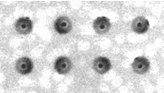
15 DSA Patterned Contact Holes for SRAM Template SEM DSA SEM 200 nm 200 nm 300mm wafer 193 nm immersion Litho Industrial compatible sol. a 3 1 Mean: 24.8 nm SD: 3.0 nm Mean: 66.4 nm SD: 6.9 nm Hole Size (nm) b AveDev-x= 0.9 nm AveDev-y= 1.2 nm Template ~ 66.4±7nm Contact hole ~ 25±3nm Centroid x ~0.9 nm Centroid y ~1.2 nm Centroid Deviation (nm) X.-Y. Bao, H. Yi H.-S. P. Wong, IEDM, p. 167, July 9, 2012

 Rotate to fit 30nm pitch 40")

16 Contact Holes for NAND (strategy) 2-hole templates for NAND A B 60x110nm 15 nm hole size 40 nm pitch (source: UBM Techinsights) Rotate to fit 30nm pitch 40 nm 30 nm 48.6 Extend to 15-nm NAND X.-Y. Bao, H. Yi H.-S. P. Wong, IEDM, p. 167, July 9, 2012
 Example of 3x-nm DRAM (Source: Chipworks) 20nm wide eye-guiding grids Shrink to 2x-nm DRAM 3-hole templates (70x145nm) 17 July 9, 2012 X.-Y. Bao, H. Yi H.-S. P. Wong, IEDM, p.")
17 Contact holes for DRAM (strategy) 3-hole templates for DRAM 70nm space 90nm pitch Storage Node Contact Bit-line Contact 145nm space 165nm pitch 3 contacts per active island (2 storage and one bitline) Example of 3x-nm DRAM (Source: Chipworks) 20nm wide eye-guiding grids Shrink to 2x-nm DRAM 3-hole templates (70x145nm) 17 July 9, 2012 X.-Y. Bao, H. Yi H.-S. P. Wong, IEDM, p. 167, 2011

18 Nangate cell library: J. Stork, TI (2007), Stanford seminar
19 Contacts for Random Logic Circuit Example: Conventional 45nm HA-X1 Layout Contact hole layout Design 1 Design 2 Source: Nangate 45nm Open Cell Library Challenges for DSA patterning Overcome resolution limits Irregular contact distribution Guiding template design Optimal template size and shape Courtesy of Jason Sweis, Cadence Design Systems 19 July 9, 2012

 unchanged No area penalty Conventional HA-X1 Layout DSA-Aware HA-X1 Layout")
20 DSA-Aware Layout: Simplifying Template Design Starting Point: Gridded Design Rule (GDR) Scan-D Flip Flop designed with Gridded Design Rules Lines: parallel, single width & pitch Contacts: positioned only at predetermined grid points Source: Transistor sizes and connections (pin-out) unchanged No area penalty Conventional HA-X1 Layout DSA-Aware HA-X1 Layout Metal 1 Poly Active Region Contact M2 vertical direction routing not shown for the sake of clarity 20 July 9, 2012
 DSA results (SEM) Scale bar: 200nm 21 July")
21 Random Logic Circuit Patterning: 1-bit Half Adder DSA-aware HA-X1 Contact Hole Layout Template defects DSA heal defects Template (SEM) DSA results (SEM) Scale bar: 200nm 21 July 9, 2012


22 Random Logic Circuit Patterning: 1-bit Half Adder Template defects Scale bar: 200nm 22 July 9, 2012


23 Random Logic Circuit Patterning: 1-bit Half Adder DSA heals defects Scale bar: 200nm 23 July 9, 2012
 DSA-aware FA-X1 Contact Hole Layout Merged templates don t affect DSA holes")

 Green histogram: represent holes in merged templates.")
24 Random Logic Circuit Patterning: 1-bit Full Adder Conventional FA-X1 (Nangate 45nm Open Cell Library) DSA-aware FA-X1 Contact Hole Layout Merged templates don t affect DSA holes overlay accuracy and size variation strongly 4 Mean: 15.0nm Std: 1.4nm 4 3 Mean: 51.1nm Std: 1.3nm 8 6 Mean Deviation-X: 0.7nm 4 Mean Deviation-Y: 0.8nm Hole Size (nm) Template Size (nm) Centroid Deviation (nm) Green histogram: represent holes in merged templates Centroid Deviation (nm) 24 July 9, 2012


25 Random Logic Circuit Patterning: 1-bit Full Adder Merged templates don t affect DSA holes overlay accuracy and size variation Green histogram: represent holes in merged templates 4 3 Mean: 15.0nm Std: 1.4nm 4 3 Mean: 51.1nm Std: 1.3nm Hole Size (nm) Template Size (nm) 8 6 Mean Deviation-X: 0.7nm 4 Mean Deviation-Y: 0.8nm 4 Scale bar: 200nm Centroid Deviation (nm) Centroid Deviation (nm) 25 July 9, 2012


26 DSA for Contact Hole Patterning DSA Evolution Infinite periodic Boundary periodic nm immersion + DSA = Extension of double-patterning 26 July 9, 2012
27 Looking Forward Defectivity 300 mm wafer, statistical data EDA tool Think OPC, DFM Application of DSA must be transparent to designers Develop DSA-aware template design rules Experiments, modeling 27 July 9, 2012

 Currently with AMAT 28")
28 Graduated Student and Post-Doc Li-Wen Chang PhD 2010 Currently with Xilinx Xinyu Bao Post-doc ( ) Currently with AMAT 28 July 9, 2012
29 Collaborators Applied Materials (Chris Bencher and team) Prof. Subhasish Mitra (Stanford, EE & CS Dept.) 29 July 9, 2012


30 Sponsors and Collaborators 30 July 9, 2012
Advanced multi-patterning and hybrid lithography techniques. Fedor G Pikus, J. Andres Torres
 Advanced multi-patterning and hybrid lithography techniques Fedor G Pikus, J. Andres Torres Outline Need for advanced patterning technologies Multipatterning (MP) technologies What is multipatterning?
Pushing 193i lithography by Joint optimization of Layout and Lithography
 Pushing 193i lithography by Joint optimization of Layout and Lithography Peter De Bisschop Imec, Leuven, Belgium Semicon Europe Messe Dresden, Germany Lithography session October 12, 2011 Semiconductor-Industry
Systematic Defect Filtering and Data Analysis Methodology for Design Based Metrology
 Systematic Defect Filtering and Data Analysis Methodology for Design Based Metrology Hyunjo Yang* a, Jungchan Kim a, Taehyeong Lee a, Areum Jung a, Gyun Yoo a, Donggyu Yim a, Sungki Park a, Toshiaki Hasebe
Continuing Moore s law
 Continuing Moore s law MARK BOHR INTEL SENIOR FELLOW, TECHNOLOGY AND MANUFACTURING GROUP DIRECTOR, PROCESS ARCHITECTURE AND INTEGRATION SEPTEMBER 19, 2017 Legal Disclaimer DISCLOSURES China Tech and Manufacturing
2. TOPOLOGICAL PATTERN ANALYSIS
 Methodology for analyzing and quantifying design style changes and complexity using topological patterns Jason P. Cain a, Ya-Chieh Lai b, Frank Gennari b, Jason Sweis b a Advanced Micro Devices, 7171 Southwest
Physical stuff (20 mins) C2S2 Workshop 7/28/06
 C2S2 Workshop 7/28/06") Physical stuff (20 mins) C2S2 Workshop 7/28/06 Clive Bittlestone TI Fellow Nagaraj NS DMTS, Roger Griesmer SMTS Carl Vickery SMTS Gopalarao Kadamati MGTS Texas Instruments Texas Instruments 2004,2005,2006
Physical stuff (20 mins) C2S2 Workshop 7/28/06 Clive Bittlestone TI Fellow Nagaraj NS DMTS, Roger Griesmer SMTS Carl Vickery SMTS Gopalarao Kadamati MGTS Texas Instruments Texas Instruments 2004,2005,2006
Low k 1 Logic Design using Gridded Design Rules
 SPIE Advanced Lithography Conference 2008 6925-68 Tela Innovations, ASML 1 Low k 1 Logic Design using Gridded Design Rules Michael C. Smayling a, Hua-yu Liu b, Lynn Cai b a Tela Innovations, Inc., 655
Approaches to the Metrology Challenges for DSA Hole
 Approaches to the Metrology Challenges for DSA Hole Masafumi Asano, Kazuto Matsuki, Tomoko Ojima, Hiroki Yonemitsu, Ayako Kawanishi, Miwa Sato 2015 Toshiba Corporation Introduction Outline Metrology for
Physical design and mask synthesis considerations for DPT
 Physical design and mask synthesis considerations for DPT Kevin Lucas, Chris Cork, John Hapli, Alex Miloslavsky Synopsys Vincent Wiaux, Staf Verhaegen IMEC Double Patterning pitch splitting 1 st trench
Packaging of Selected Advanced Logic in 2x and 1x nodes. 1 I TechInsights
 Packaging of Selected Advanced Logic in 2x and 1x nodes 1 I TechInsights Logic: LOGIC: Packaging of Selected Advanced Devices in 2x and 1x nodes Xilinx-Kintex 7XC 7 XC7K325T TSMC 28 nm HPL HKMG planar
AltaSens A5262-4T 4.5 Megapixel CMOS Image Sensor 0.18 µm IBM Process
 AltaSens A5262-4T 4.5 Megapixel CMOS Image Sensor 0.18 µm IBM Process Imager Process Review For comments, questions, or more information about this report, or for any additional technical needs concerning
Taurus-Process. Multidimensional Process Simulation SYSTEMS PRODUCTS LOGICAL PRODUCTS PHYSICAL IMPLEMENTATION SIMULATION AND ANALYSIS LIBRARIES TCAD
 SYSTEMS PRODUCTS LOGICAL PRODUCTS PHYSICAL IMPLEMENTATION SIMULATION AND ANALYSIS LIBRARIES TCAD Aurora DFM WorkBench Davinci Medici Raphael Raphael-NES Silicon Early Access TSUPREM-4 Taurus-Device Taurus-Lithography
32nm and below Logic Patterning using Optimized Illumination and Double Patterning
 32nm and below Logic Patterning using Optimized Illumination and Double Patterning Michael C. Smayling* a, Valery Axelrad b a Tela Innovations, Inc., 655 Technology Pkwy, Suite 150, Campbell, CA, USA 95008
ASIC design flow considering lithography-induced effects
 DESIGN FOR MANUFACTURABILITY ASIC design flow considering lithography-induced effects K. Cao and J. Hu Abstract: As VLSI technology scales towards 65 nm and beyond, both timing and power performance of
Taming the Challenges of Advanced-Node Design. Tom Beckley Sr. VP of R&D, Custom IC and Signoff, Silicon Realization Group ISQED 2012 March 20, 2012
 Taming the Challenges of Advanced-Node Design Tom Beckley Sr. VP of R&D, Custom IC and Signoff, Silicon Realization Group ISQED 2012 March 20, 2012 The custom design community Designers ( Relaxed attitude
Composite Layout CS/EE N-type from the top. N-type Transistor. Diffusion Mask. Polysilicon Mask
 Composite Layout CS/EE 6710 Introduction to Layout Inverter Layout Example Layout Design Rules Drawing the mask layers that will be used by the fabrication folks to make the devices Very different from
Design Methodologies. Full-Custom Design
 Design Methodologies Design styles Full-custom design Standard-cell design Programmable logic Gate arrays and field-programmable gate arrays (FPGAs) Sea of gates System-on-a-chip (embedded cores) Design
NVIDIA Tegra T20-H-A2 Application Processor TSMC 40 nm Low Power CMOS Process
 NVIDIA Tegra T20-H-A2 Application Processor TSMC 40 nm Low Power CMOS Process Structural Analysis 3685 Richmond Road, Suite 500, Ottawa, ON K2H 5B7 Canada Tel: 613-829-0414 www.chipworks.com Structural
Circuits. L3: Fabrication and Layout -1 ( ) B. Mazhari Dept. of EE, IIT Kanpur. B. Mazhari, IITK. G-Number
 B. Mazhari Dept. of EE, IIT Kanpur. B. Mazhari, IITK. G-Number") EE60: CMOS Analog Circuits L: Fabrication and Layout - (8.8.0) B. Mazhari Dept. of EE, IIT Kanpur Suppose we have a Silicon wafer which is P-type and we wish to create a region within it which is N-type
EE60: CMOS Analog Circuits L: Fabrication and Layout - (8.8.0) B. Mazhari Dept. of EE, IIT Kanpur Suppose we have a Silicon wafer which is P-type and we wish to create a region within it which is N-type
EE582 Physical Design Automation of VLSI Circuits and Systems
 EE582 Prof. Dae Hyun Kim School of Electrical Engineering and Computer Science Washington State University Preliminaries Table of Contents Semiconductor manufacturing Problems to solve Algorithm complexity
Regularity for Reduced Variability
 Regularity for Reduced Variability Larry Pileggi Carnegie Mellon pileggi@ece.cmu.edu 28 July 2006 CMU Collaborators Andrzej Strojwas Slava Rovner Tejas Jhaveri Thiago Hersan Kim Yaw Tong Sandeep Gupta
Stitch Aware Detailed Placement for Multiple E-Beam Lithography
 Stitch Aware Detailed Placement for Multiple E-Beam Lithography Yibo Lin 1, Bei Yu 2, Yi Zou 1,3, Zhuo Li 4, Charles J. Alpert 4, and David Z. Pan 1 1 ECE Department, University of Texas at Austin 2 CSE
Addressable Test Chip Technology for IC Design and Manufacturing. Dr. David Ouyang CEO, Semitronix Corporation Professor, Zhejiang University 2014/03
 Addressable Test Chip Technology for IC Design and Manufacturing Dr. David Ouyang CEO, Semitronix Corporation Professor, Zhejiang University 2014/03 IC Design & Manufacturing Trends Both logic and memory
Vdd Programmable and Variation Tolerant FPGA Circuits and Architectures
 Vdd Programmable and Variation Tolerant FPGA Circuits and Architectures Prof. Lei He EE Department, UCLA LHE@ee.ucla.edu Partially supported by NSF. Pathway to Power Efficiency and Variation Tolerance
Samsung K9GAG08U0M-PCB0 16 Gbit Multi-Level Cell (MLC) 51 nm Process Technology NAND Flash Memory
 51 nm Process Technology NAND Flash Memory") Samsung K9GAG08U0M-PCB0 16 Gbit Multi-Level Cell (MLC) 51 nm Process Technology NAND Flash Memory Structural Analysis with Additional Layout Feature Analysis For comments, questions, or more information
Samsung K9GAG08U0M-PCB0 16 Gbit Multi-Level Cell (MLC) 51 nm Process Technology NAND Flash Memory Structural Analysis with Additional Layout Feature Analysis For comments, questions, or more information
Broadcom BCM7405 HD Video/Audio System-on-Chip (SoC)
") Broadcom BCM7405 HD Video/Audio System-on-Chip (SoC) For comments, questions, or more information about this report, or for any additional technical needs concerning semiconductor technology, please call
Broadcom BCM7405 HD Video/Audio System-on-Chip (SoC) For comments, questions, or more information about this report, or for any additional technical needs concerning semiconductor technology, please call
A tutorial for the CAD program LayoutEditor. by Jürgen Thies, Juspertor UG, Munich
 A tutorial for the CAD program LayoutEditor LayoutEditor is available from www.layouteditor.net by Jürgen Thies, Juspertor UG, Munich M. Rooks, Yale University Common terminology Layers Cells Top-level
ECE520 VLSI Design. Lecture 1: Introduction to VLSI Technology. Payman Zarkesh-Ha
 ECE520 VLSI Design Lecture 1: Introduction to VLSI Technology Payman Zarkesh-Ha Office: ECE Bldg. 230B Office hours: Wednesday 2:00-3:00PM or by appointment E-mail: pzarkesh@unm.edu Slide: 1 Course Objectives
Applications of DSA for lithography
 Applications of DSA for lithography Yoshi Hishiro, Takehiko Naruoka, JSR Micro Inc. Yuusuke Anno JSR Micro NV. Hayato Namai, Fumihiro Toyokawa, Shinya Minegishi, Yuuji Namie, Tomoki Nagai, Kentaro Goto,
Digital Integrated CircuitDesign
 Digital Integrated CircuitDesign Lecture 8 Design Rules Adib Abrishamifar EE Department IUST Contents Design Rules CMOS Process Layers Intra-Layer Design Rules Via s and Contacts Select Layer Example Cell
On-Chip Variation (OCV) Kunal Ghosh
 Kunal Ghosh") On-Chip Variation (OCV) Kunal Ghosh Ever thought what s an interviewer s favorite questions to rip you off all my previous ebooks. And On-Chip Variation (OCV) is one of them, specifically for Static Timing
On-Chip Variation (OCV) Kunal Ghosh Ever thought what s an interviewer s favorite questions to rip you off all my previous ebooks. And On-Chip Variation (OCV) is one of them, specifically for Static Timing
Design Rule Optimization of Regular layout for Leakage Reduction in Nanoscale Design
 Design Rule Optimization of Regular layout for Leakage Reduction in Nanoscale Design Anupama R. Subramaniam, Ritu Singhal, Chi-Chao Wang, Yu Cao Department of Electrical Engineering, Arizona State University,
A Framework for Systematic Evaluation and Exploration of Design Rules
 A Framework for Systematic Evaluation and Exploration of Design Rules Rani S. Ghaida* and Prof. Puneet Gupta EE Dept., University of California, Los Angeles (rani@ee.ucla.edu), (puneet@ee.ucla.edu) Work
EE241 - Spring 2007 Advanced Digital Integrated Circuits. Announcements
 EE241 - Spring 2007 Advanced Digital Integrated Circuits Lecture 22: SRAM Announcements Homework #4 due today Final exam on May 8 in class Project presentations on May 3, 1-5pm 2 1 Class Material Last
An Introduction to Programmable Logic
 Outline An Introduction to Programmable Logic 3 November 24 Transistors Logic Gates CPLD Architectures FPGA Architectures Device Considerations Soft Core Processors Design Example Quiz Semiconductors Semiconductor
Development of innovative ALD materials for high density 3D integrated capacitors
 Development of innovative ALD materials for high density 3D integrated capacitors Malte Czernohorsky General Trend: System miniaturization Integration of passive components Capacitors Inductors Resistors
CENG 4480 L09 Memory 3
 CENG 4480 L09 Memory 3 Bei Yu Chapter 11 Memories Reference: CMOS VLSI Design A Circuits and Systems Perspective by H.E.Weste and D.M.Harris 1 Memory Arrays Memory Arrays Random Access Memory Serial Access
Texas Instruments TMX320TCI6488ZUNV Baseband Processor System on a Chip
 Texas Instruments TMX320TCI6488ZUNV Baseband Processor System on a Chip Structural Analysis For comments, questions, or more information about this report, or for any additional technical needs concerning
Pattern-based analytics to estimate and track yield risk of designs down to 7nm
 DAC 2017 Pattern-based analytics to estimate and track yield risk of designs down to 7nm JASON CAIN, MOUTAZ FAKHRY (AMD) PIYUSH PATHAK, JASON SWEIS, PHILIPPE HURAT, YA-CHIEH LAI (CADENCE) INTRODUCTION
Nokia N90 (Toshiba ET8EA3-AS) 2.0 Megapixel CMOS Image Sensor Process Review
 2.0 Megapixel CMOS Image Sensor Process Review") November 21, 2005 Nokia N90 (Toshiba ET8EA3-AS) 2.0 Megapixel CMOS Image Sensor Process Review For comments, questions, or more information about this report, or for any additional technical needs concerning
November 21, 2005 Nokia N90 (Toshiba ET8EA3-AS) 2.0 Megapixel CMOS Image Sensor Process Review For comments, questions, or more information about this report, or for any additional technical needs concerning
A New Methodology for Interconnect Parasitic Extraction Considering Photo-Lithography Effects
 A New Methodology for Interconnect Parasitic Extraction Considering Photo-Lithography Effects Ying Zhou, Yuxin Tian, Weiping Shi Texas A&M University Zhuo Li Pextra Corporation Frank Liu IBM Austin Research
CMP Model Application in RC and Timing Extraction Flow
 INVENTIVE CMP Model Application in RC and Timing Extraction Flow Hongmei Liao*, Li Song +, Nickhil Jakadtar +, Taber Smith + * Qualcomm Inc. San Diego, CA 92121 + Cadence Design Systems, Inc. San Jose,
Advanced Flash Technology Status, Scaling Trends & Implications to Enterprise SSD Technology Enablement
 Advanced Flash Technology Status, Scaling Trends & Implications to Enterprise SSD Technology Enablement Jung H. Yoon & Gary A. Tressler IBM Corporation Aug 21, 2012 Santa Clara, CA 1 Outline Si Technology
EECS 598: Integrating Emerging Technologies with Computer Architecture. Lecture 10: Three-Dimensional (3D) Integration
 Integration") 1 EECS 598: Integrating Emerging Technologies with Computer Architecture Lecture 10: Three-Dimensional (3D) Integration Instructor: Ron Dreslinski Winter 2016 University of Michigan 1 1 1 Announcements
1 EECS 598: Integrating Emerging Technologies with Computer Architecture Lecture 10: Three-Dimensional (3D) Integration Instructor: Ron Dreslinski Winter 2016 University of Michigan 1 1 1 Announcements
STMicroelectronics STM32F103ZET6 32 Bit MCU. Advanced Functional Analysis
 Advanced Functional Analysis For comments, questions, or more information about this report, or for any additional technical needs concerning semiconductor technology, please call Sales at Chipworks. 3685
FPGA Programming Technology
 FPGA Programming Technology Static RAM: This Xilinx SRAM configuration cell is constructed from two cross-coupled inverters and uses a standard CMOS process. The configuration cell drives the gates of
Memory in Digital Systems
 MEMORIES Memory in Digital Systems Three primary components of digital systems Datapath (does the work) Control (manager) Memory (storage) Single bit ( foround ) Clockless latches e.g., SR latch Clocked
CS310 Embedded Computer Systems. Maeng
 1 INTRODUCTION (PART II) Maeng Three key embedded system technologies 2 Technology A manner of accomplishing a task, especially using technical processes, methods, or knowledge Three key technologies for
Sample Table of Contents
 Sample Table of Contents from System-on-Chip (SoC) For any additional technical needs concerning semiconductor and electronics technology, please call Sales at Chipworks. 3685 Richmond Road, Suite 500,
Memjet ML Printhead from the RapidX1 Color Label Printer
 ML210700 Printhead from the RapidX1 Color Label Printer MEMS Process Review 3685 Richmond Road, Suite 500, Ottawa, ON K2H 5B7 Canada Tel: 613-829-0414 www.chipworks.com MEMS Process Review Some of the
ECE 485/585 Microprocessor System Design
 Microprocessor System Design Lecture 4: Memory Hierarchy Memory Taxonomy SRAM Basics Memory Organization DRAM Basics Zeshan Chishti Electrical and Computer Engineering Dept Maseeh College of Engineering
More Course Information
 More Course Information Labs and lectures are both important Labs: cover more on hands-on design/tool/flow issues Lectures: important in terms of basic concepts and fundamentals Do well in labs Do well
Cell Libraries and Design Hierarchy. Instructor S. Demlow ECE 410 February 1, 2012
 Cell Libraries and Design Hierarchy Instructor S. Demlow ECE 410 February 1, 2012 Stick Diagrams Simplified NAND Layout Simplified NOR Layout Metal supply rails blue n and p Active green Poly gates red
Model Based Guiding Pattern Synthesis for on-target and robust assembly of Via and Contact layers using DSA
 Model Based Guiding Pattern Synthesis for on-target and robust assembly of Via and Contact layers using DSA Joydeep Mitra 1, Andres Torres 1, Yuansheng Ma 1, and David Z Pan 2 1 Mentor Graphics Corporation
Design for Manufacturability: From Ad Hoc Solution To Extreme Regular Design
 Design for Manufacturability: From Ad Hoc Solution To Extreme Regular Design Bei Yu Department of Computer Science and Engineering The Chinese University of Hong Kong 1 Introduction and Motivation In very
Digital Integrated Circuits (83-313) Lecture 2: Technology and Standard Cell Layout
 Lecture 2: Technology and Standard Cell Layout") Digital Integrated Circuits (83-313) Lecture 2: Technology and Standard Cell Layout Semester B, 2016-17 Lecturer: Dr. Adam Teman TAs: Itamar Levi, Robert Giterman 26 March 2017 Disclaimer: This course
Digital Integrated Circuits (83-313) Lecture 2: Technology and Standard Cell Layout Semester B, 2016-17 Lecturer: Dr. Adam Teman TAs: Itamar Levi, Robert Giterman 26 March 2017 Disclaimer: This course
ELCT 912: Advanced Embedded Systems
 Advanced Embedded Systems Lecture 2: Memory and Programmable Logic Dr. Mohamed Abd El Ghany, Memory Random Access Memory (RAM) Can be read and written Static Random Access Memory (SRAM) Data stored so
Design Factors Affecting Laser Cutting Parameters Line width Wider lines more heat flow Lines affect spot size larger line: wider spot Lines much
 Design Factors Affecting Laser Cutting Parameters Line width Wider lines more heat flow Lines affect spot size larger line: wider spot Lines much larger than spot size Require several positions and laser
CS24: INTRODUCTION TO COMPUTING SYSTEMS. Spring 2017 Lecture 13
 CS24: INTRODUCTION TO COMPUTING SYSTEMS Spring 2017 Lecture 13 COMPUTER MEMORY So far, have viewed computer memory in a very simple way Two memory areas in our computer: The register file Small number
EUV Lithography and Overlay Control
 YMS Magazine DECEMBER 2017 EUV Lithography and Overlay Control Efi Megged, Mark Wylie and Cathy Perry-Sullivan L A-Tencor Corporation One of the key parameters in IC fabrication is overlay the accuracy
MEMORIES. Memories. EEC 116, B. Baas 3
 MEMORIES Memories VLSI memories can be classified as belonging to one of two major categories: Individual registers, single bit, or foreground memories Clocked: Transparent latches and Flip-flops Unclocked:
Layout Analysis Embedded Memory
 Sample Report For any additional technical needs concerning semiconductor and electronics technology, please call Sales at Chipworks. 3685 Richmond Road, Suite 500, Ottawa, ON K2H 5B7, Canada Tel: 613.829.0414
STMicroelectronics STM32F103ZET6 32 Bit MCU Embedded NOR Flash
 32 Bit MCU Embedded NOR Flash Process Review For comments, questions, or more information about this report, or for any additional technical needs concerning semiconductor technology, please call Sales
Design rule illustrations for the AMI C5N process can be found at:
 Cadence Tutorial B: Layout, DRC, Extraction, and LVS Created for the MSU VLSI program by Professor A. Mason and the AMSaC lab group. Revised by C Young & Waqar A Qureshi -FS08 Document Contents Introduction
The Evolving Semiconductor Technology Landscape and What it Means for Lithography. Scotten W. Jones President IC Knowledge LLC
 The Evolving Semiconductor Technology Landscape and What it Means for Lithography Scotten W. Jones President IC Knowledge LLC Outline NAND DRAM Logic Conclusion 2 NAND Linewidth Trend 2D to 3D For approximately
Recent Research and Emerging Challenges in Physical Design for Manufacturability/Reliability
 Recent Research and Emerging Challenges in Physical Design for Manufacturability/Reliability Chung-Wei Lin 1, Ming-Chao Tsai 2, Kuang-Yao Lee 2, Tai-Chen Chen 1, Ting-Chi Wang 2, and Yao-Wen Chang 1 1
Challenges in Manufacturing of optical and EUV Photomasks Martin Sczyrba
 Challenges in Manufacturing of optical and EUV Photomasks Martin Sczyrba Advanced Mask Technology Center Dresden, Germany Senior Member of Technical Staff Advanced Mask Technology Center Dresden Key Facts
Integrated Circuits & Systems
 Federal University of Santa Catarina Center for Technology Computer Science & Electronics Engineering Integrated Circuits & Systems INE 5442 Lecture 23-1 guntzel@inf.ufsc.br Semiconductor Memory Classification
Design Methodologies and Tools. Full-Custom Design
 Design Methodologies and Tools Design styles Full-custom design Standard-cell design Programmable logic Gate arrays and field-programmable gate arrays (FPGAs) Sea of gates System-on-a-chip (embedded cores)
! Memory Overview. ! ROM Memories. ! RAM Memory " SRAM " DRAM. ! This is done because we can build. " large, slow memories OR
 ESE 57: Digital Integrated Circuits and VLSI Fundamentals Lec 2: April 5, 26 Memory Overview, Memory Core Cells Lecture Outline! Memory Overview! ROM Memories! RAM Memory " SRAM " DRAM 2 Memory Overview
On Comparing Conventional and Electrically Driven OPC Techniques
 On Comparing Conventional and Electrically Driven OPC Techniques Dominic Reinhard and Puneet Gupta EE Dept., University of California, Los Angeles {dominicr,puneet}@ee.ucla.edu ABSTRACT This paper compares
Investigation of Diffusion Rounding for. Investigation of Diffusion Rounding for. Post-Lithography Analysis. Puneet Gupta 1, Andrew B.
 Investigation of Diffusion Rounding for Investigation of Diffusion Rounding for Post-Lithography Analysis Puneet Gupta 1, Andrew B. Kahng 2, Youngmin Kim 3*, Saumil Shah 4, and Dennis Sylvester 3 1 University
FABRICATION TECHNOLOGIES
 FABRICATION TECHNOLOGIES DSP Processor Design Approaches Full custom Standard cell** higher performance lower energy (power) lower per-part cost Gate array* FPGA* Programmable DSP Programmable general
Microelettronica. J. M. Rabaey, "Digital integrated circuits: a design perspective" EE141 Microelettronica
 Microelettronica J. M. Rabaey, "Digital integrated circuits: a design perspective" Introduction Why is designing digital ICs different today than it was before? Will it change in future? The First Computer
Manufacturing Challenges and their Implications on Design
 Manufacturing Challenges and their Implications on Design Phiroze Parakh, Ph.D 45nm/32nm Design Challenges MANUFACTURING VARIATIONS PROCESS & DESIGN VARIATIONS LARGE DESIGNS LOW POWER The Evolution of
ECE 261: Full Custom VLSI Design
 ECE 261: Full Custom VLSI Design Prof. James Morizio Dept. Electrical and Computer Engineering Hudson Hall Ph: 201-7759 E-mail: jmorizio@ee.duke.edu URL: http://www.ee.duke.edu/~jmorizio Course URL: http://www.ee.duke.edu/~jmorizio/ece261/261.html
VLSI Lab Tutorial 3. Virtuoso Layout Editing Introduction
 VLSI Lab Tutorial 3 Virtuoso Layout Editing Introduction 1.0 Introduction The purpose of this lab tutorial is to guide you through the design process in creating a custom IC layout for your CMOS inverter
Texas Instruments S W Digital Micromirror Device
 Texas Instruments S1076-6318W MEMS Process Review with Supplementary TEM Analysis For comments, questions, or more information about this report, or for any additional technical needs concerning semiconductor
Introduction to SRAM. Jasur Hanbaba
 Introduction to SRAM Jasur Hanbaba Outline Memory Arrays SRAM Architecture SRAM Cell Decoders Column Circuitry Non-volatile Memory Manufacturing Flow Memory Arrays Memory Arrays Random Access Memory Serial
Simultaneous OPC- and CMP-Aware Routing Based on Accurate Closed-Form Modeling
 Simultaneous OPC- and CMP-Aware Routing Based on Accurate Closed-Form Modeling Shao-Yun Fang, Chung-Wei Lin, Guang-Wan Liao, and Yao-Wen Chang March 26, 2013 Graduate Institute of Electronics Engineering
Memory Design I. Semiconductor Memory Classification. Read-Write Memories (RWM) Memory Scaling Trend. Memory Scaling Trend
 Memory Scaling Trend. Memory Scaling Trend") Array-Structured Memory Architecture Memory Design I Professor hris H. Kim University of Minnesota Dept. of EE chriskim@ece.umn.edu 2 Semiconductor Memory lassification Read-Write Memory Non-Volatile Read-Write
Array-Structured Memory Architecture Memory Design I Professor hris H. Kim University of Minnesota Dept. of EE chriskim@ece.umn.edu 2 Semiconductor Memory lassification Read-Write Memory Non-Volatile Read-Write
DSA: How far have we come and how much further is left to go? Darron Jurajda
 DSA: How far have we come and how much further is left to go? Darron Jurajda Semiconductor Business Unit Director, Brewer Science Outline Background of DSA at Brewer Science DSA historical progress Hype
QUESTION BANK FOR TEST
 CSCI 2121 Computer Organization and Assembly Language PRACTICE QUESTION BANK FOR TEST 1 Note: This represents a sample set. Please study all the topics from the lecture notes. Question 1. Multiple Choice
Designing into a Foundry Low Power High-k Metal Gate 28nm CMOS Solution for High-Performance Analog Mixed Signal and Mobile Applications
 Designing into a Foundry Low Power High-k Metal Gate 28nm CMOS Solution for High-Performance Analog Mixed Signal and Mobile Applications A Collaborative White Paper by RAMBUS and GLOBALFOUNDRIES W h i
Development of a Design & Manufacturing Environment for Reliable and Cost- Effective PCB Embedding Technology
 Development of a Design & Manufacturing Environment for Reliable and Cost- Effective PCB Embedding Technology Outline Introduction CAD design tools for embedded components Thermo mechanical design rules
Chapter 5: ASICs Vs. PLDs
 Chapter 5: ASICs Vs. PLDs 5.1 Introduction A general definition of the term Application Specific Integrated Circuit (ASIC) is virtually every type of chip that is designed to perform a dedicated task.
Unit 6 1.Random Access Memory (RAM) Chapter 3 Combinational Logic Design 2.Programmable Logic
 Chapter 3 Combinational Logic Design 2.Programmable Logic") EE 200: Digital Logic Circuit Design Dr Radwan E Abdel-Aal, COE Unit 6.Random Access Memory (RAM) Chapter 3 Combinational Logic Design 2. Logic Logic and Computer Design Fundamentals Part Implementation
EE 200: Digital Logic Circuit Design Dr Radwan E Abdel-Aal, COE Unit 6.Random Access Memory (RAM) Chapter 3 Combinational Logic Design 2. Logic Logic and Computer Design Fundamentals Part Implementation
Abbas El Gamal. Joint work with: Mingjie Lin, Yi-Chang Lu, Simon Wong Work partially supported by DARPA 3D-IC program. Stanford University
 Abbas El Gamal Joint work with: Mingjie Lin, Yi-Chang Lu, Simon Wong Work partially supported by DARPA 3D-IC program Stanford University Chip stacking Vertical interconnect density < 20/mm Wafer Stacking
SYNTHESIS FOR ADVANCED NODES
 SYNTHESIS FOR ADVANCED NODES Abhijeet Chakraborty Janet Olson SYNOPSYS, INC ISPD 2012 Synopsys 2012 1 ISPD 2012 Outline Logic Synthesis Evolution Technology and Market Trends The Interconnect Challenge
Magic Technology Manual #1: NMOS
 Magic Technology Manual #1: NMOS John Ousterhout Computer Science Division Electrical Engineering and Computer Sciences University of California Berkeley, CA 970 (Warning: Process details often change.
Tutorial on Design For Manufacturability for Physical Design
 Tutorial on Design For Manufacturability for Physical Design Andrzej J. Strojwas PDF Solutions Inc., San Jose, CA & Carnegie Mellon University, Pittsburgh, PA 2005 ISPD, San Francisco, CA April 5, 2005
Cadence Tutorial 2: Layout, DRC/LVS and Circuit Simulation with Extracted Parasitics
 Cadence Tutorial 2: Layout, DRC/LVS and Circuit Simulation with Extracted Parasitics Introduction This tutorial describes how to generate a mask layout in the Cadence Virtuoso Layout Editor. Use of DIVA
Sigma Designs SMP8642 Secure Media Processor
 Sigma Designs SMP8642 Advanced Functional Analysis 3685 Richmond Road, Suite 500, Ottawa, ON K2H 5B7 Canada Tel: 613-829-0414 www.chipworks.com Advanced Functional Analysis Some of the information in this
Memory in Digital Systems
 MEMORIES Memory in Digital Systems Three primary components of digital systems Datapath (does the work) Control (manager) Memory (storage) Single bit ( foround ) Clockless latches e.g., SR latch Clocked
+1 (479)
") Memory Courtesy of Dr. Daehyun Lim@WSU, Dr. Harris@HMC, Dr. Shmuel Wimer@BIU and Dr. Choi@PSU http://csce.uark.edu +1 (479) 575-6043 yrpeng@uark.edu Memory Arrays Memory Arrays Random Access Memory Serial
Memory Courtesy of Dr. Daehyun Lim@WSU, Dr. Harris@HMC, Dr. Shmuel Wimer@BIU and Dr. Choi@PSU http://csce.uark.edu +1 (479) 575-6043 yrpeng@uark.edu Memory Arrays Memory Arrays Random Access Memory Serial
Programming Characteristics on Three-Dimensional NAND Flash Structure Using Edge Fringing Field Effect
 JOURNAL OF SEMICONDUCTOR TECHNOLOGY AND SCIENCE, VOL.14, NO.5, OCTOBER, 2014 http://dx.doi.org/10.5573/jsts.2014.14.5.537 Programming Characteristics on Three-Dimensional NAND Flash Structure Using Edge
Layout Analysis I/O. Analysis from an HD Video/Audio SoC
 Sample Report Analysis from an HD Video/Audio SoC For any additional technical needs concerning semiconductor and electronics technology, please call Sales at Chipworks. 3685 Richmond Road, Suite 500,
A novel methodology for Litho-to-Etch Pattern Fidelity Correction for SADP Process
 A novel methodology for Litho-to-Etch Pattern Fidelity Correction for SADP Process Shr-Jia Chen* a, Yu-Cheng Chang a, Arthur Lin b, Yi-Shiang Chang a, Chia-Chi Lin a, Jun-Cheng Lai a a Powerchip Technology
Industrial Example I Semiconductor Manufacturing Photolithography Can you tell me anything about this data!
 Can you tell me anything about this data! 1 In Semiconductor Manufacturing the Photolithography process steps are very critical to ensure proper circuit and device performance. Without good CD (critical
Three-Dimensional Integrated Circuits: Performance, Design Methodology, and CAD Tools
 Three-Dimensional Integrated Circuits: Performance, Design Methodology, and CAD Tools Shamik Das, Anantha Chandrakasan, and Rafael Reif Microsystems Technology Laboratories Massachusetts Institute of Technology