Cell-Based Design Flow. TA : 吳廸優
|
|
|
- Audra Haynes
- 5 years ago
- Views:
Transcription


1 Cell-Based Design Flow TA : 吳廸優 dywu@viplab.cs.nctu.edu.tw 1

2 Outline Overview Design Flow Stage 1 RTL Development Synthesis Gate Level Simulation Design Flow Stage 2 Placement and Routing Post Layout Simulation 2


3 Cell-based Design Flow Overview A design flow is a set of procedures that allows designers to progress from a specification for a chip to the final chip implementation in an error-free way. 3


 netlist file to run the Auto")


4 Source: CM: 5086 VLSI Design Lab Cell-based Design Flow Stage 1 Implement your own verilog program Need to pass the provided testbench Synthesis your logic with provided (or modify by yourself) tcl file Stage 2 Use your(provided) netlist file to run the Auto Place and Route (APR) flow Specification Development System Models RTL code development Functional Verification Synthesis Timing Verification Physical Synthesis/Place and Route Physical Verification System Architecture RTL Synthesis Physical Design Prototype Build and Test 4 System Integration and Software Test
5 Cell-based Design Tool System Architecture/SW simulation C/C++, Matlab, System C, System Verilog RTL simulation/debug NC-Verilog, NC-VHDL, ModelSim, Verdi(nWave) (without delay) Synthesis RTL Compiler, Design Compiler, Power Compiler Gate level simulation/debug NC-Verilog, NC-VHDL, ModelSim, Verdi(nWave) (with delay) Physical Design SoC Encounter, Astro, IC Compiler Others PrimePower, Calibre, Nanosim 5
6 Outline Overview Design Flow Stage 1 RTL Development Synthesis Gate Level Simulation Design Flow Stage 2 Placement and Routing Post Layout Simulation 6
7 RTL Development Development / simulation NC-verilog $ncverilog + <your_testbench_file> 7
; nwave $nwave (Verdi -nwave) 8")
8 RTL Development Check the simulation output Dump waveform from testbench when simulation $fsdbdumpfile( MAC.fsdb ); nwave $nwave (Verdi -nwave) 8
9 RTL Development Verilog dump related command VCD file format(value Change Dump) $dumpfile( output.vcd ); $dumpvars; FSDB file format(from Novas) $fsdbdumpfile( output.fsdb ); $fsdbdumpvars; Fsdb file is the input of Verdi Verdi(debussy): a powerful debugging tool provided by NOVAS $ Verdi 9


10 Verdi from NOVAS $ Verdi & File->Import Design ->From File ->TESTBED.v ->Add ->OK RTL Development 10
11 Source: CIC Jan.08 Design Compiler Synthesis Synthesis=translation+ optimization+ mapping Residue = 16 h0000; If(high_bits==2 b10) residue = state_table[i]; Else state_table[i] = 16 h0000; HDL Source(RTL) Translate(HDL Compiler) Optimize + Map (Design Compiler) NO Timing Info => Generic Boolean Timing Info => Target Technology 11

12 Synthesis Design Compiler It synthesizes your designs (Verilog) into optimized technology-dependent, gate-level designs. Use Design Compiler GUI Startup x-win ( or any other X terminal application) $design_vision (dv) 12
13 Synthesis Environment Setup /home directory/.cshrc : set path and license of synthesis tool /your working directory/.synopsys_dc.setup : setup technology file, designware library file etc Use DC-TCL script file(.tcl) Set design constraints $dv -f syn.tcl 13
 For")
14 Synthesis Detail of.synopsys_dc.setup ASIC Technology file (cell library) For schematic For Designware 14


15 Synthesis Modify the syn.tcl Your Design Name TOP Module Name Set wire delay model Setup & hold time library 15


16 Synthesis 16

17 Synthesis SDC file : synopsys design constrain Setup input/output delay and loading SDF file : standard delay format Setup the rising/holding/falling time for each cell of your design 17
18 Synthesis Put the RTL file,.synopsys_dc.setup and syn.tcl to your working directory, or assert the setup commands by hand, while synthesis. Under your working directory, make new directories, Report and Netlist, for saving synthesis reports. 18
 command command Command return")
19 Synthesis Output result Command return result(error) command command Command return result(done) 19
20 Synthesis The synthesis information is in your Report directory timing.txt 20
21 Gate Level Simulation Verify your synthesis result Modify your testbench (TESTBED.v) `include./netlist/seq_mac16_syn.v sdf_annotate(./netlist/seq_mac16_syn.sdf, top) $ncverilog + <your_testbench_file> + -v <Tech_verilog_file> 21

22 Gate Level Simulation Check the simulation output nwave $nwave (Verdi -nwave) 22
23 Outline Overview Design Flow Stage 1 RTL Development Synthesis Gate Level Simulation Design Flow Stage 2 Placement and Routing Post Layout Simulation 23
: IO Placement,")
24 SOC Encounter Placing & Routing Flow Netlist(verilog) Timing Constrain(sdc) IO Constrain IO, P/G Placement Specify floorplan Power Planning Amoeba Placement Timing Analysis Pre-CTS Optimize Power Route Clock Tree Synthesis Timing Analysis Post-CTS Optimize Power Analysis SI Driven Route Timing/SI Analysis Post-Route Optimize GDS file Netlist, DEF 4 Main Step (must be in order): IO Placement, Cell Placement, CTS, SI Driven Routing 24 Source: CIC Jan. 2009, SoC Encounter

25 Basic View $encounter Floorplan view Ameoba view Physical view 25


26 Design -> Design Import Project Setup netlist Cell Library Physical Library IO Map file 26

27 IO, Power/Ground Placement Floorplan -> Connect Global Nets 27

28 Floorplan Floorplan -> Specify Floorplan 28


29 Power Planning Power -> Power Planning -> Add Rings 29


30 Cell Placement Place -> Standard Cell And Blocks 30


31 Route -> Special Route Power Route 31


32 Pre-CTS Timing Timing -> Analyze Timing -> Pre-CTS -> Setup If timing is not meet, Timing -> Optimize -> Pre-CTS 32 -> setup

33 Add Tie Hi/Lo cell Place -> Tie HI/LO -> Add 33


34 Clock -> Design Clock Clock Tree Synthesis 34

35 Post-CTS Timing Timing -> Analyze Timing -> Post-CTS -> setup/hold If timing is not meet, Timing -> Optimize -> Post-CTS 35 -> setup/hold


36 Route -> NanoRoute SI Driven Route 36

37 Post-Route Timing Timing -> Analyze Timing -> Post-Route -> setup/hold If timing is not meet, Timing -> Optimize -> Post-Route 37 -> setup/hold
38 Result Analysis Final step DRC LVS verification Save file Verify -> Verify Connectivity Verify -> Verify Geometry Design -> Save Design As -> SoCE -> Seq_MAC16_final.enc Design -> Save -> Netlist -> Seq_MAC16_LAYOUT.v Timing -> Calculate Delay -> disable ideal Clock -> Seq_MAC16_LAYOUT.sdf 38
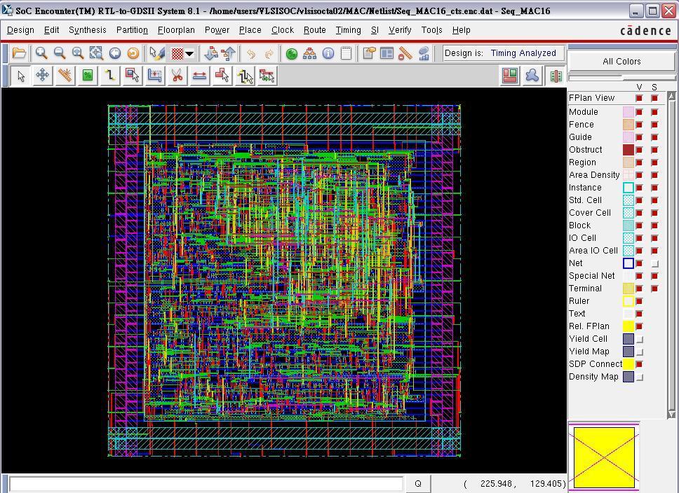
39 Final 39
40 Post Layout Simulation Verify your physical design result Modify your testbench (TESTBED.v) `include./netlist/seq_mac16_layout.v sdf_annotate(./netlist/seq_mac16_layout.sdf, top) $ncverilog + <your_testbench_file> + -v <Tech_verilog_file> 40
Cell-Based Design Flow. 林丞蔚
 Cell-Based Design Flow 林丞蔚 cultom@viplab.cs.nctu.edu.tw 1 Outline Overview Design Flow 1 RTL Development Synthesis Gate Level Simulation Design Flow 2 Placement and Routing Example Design IC Contest 2006
Cell-Based IC Physical Design & Verification SOC Encounter. Advisor : 李昆忠 Presenter : 蕭智元
 Cell-Based IC Physical Design & Verification SOC Encounter Advisor : 李昆忠 Presenter : 蕭智元 Reference: SOC Encounter Training Manual, 2007, edited by CIC. Introduction We ll use some EDA tools to transform
An overview of standard cell based digital VLSI design
 An overview of standard cell based digital VLSI design Implementation of the first generation AsAP processor Zhiyi Yu and Tinoosh Mohsenin VCL Laboratory UC Davis Outline Overview of standard cellbased
Synthesis and APR Tools Tutorial
 Synthesis and APR Tools Tutorial (Last updated: Oct. 26, 2008) Introduction This tutorial will get you familiarized with the design flow of synthesizing and place and routing a Verilog module. All the
EE 330 Laboratory Experiment Number 11
 EE 330 Laboratory Experiment Number 11 Design and Simulation of Digital Circuits using Hardware Description Languages Fall 2017 Contents Purpose:... 3 Background... 3 Part 1: Inverter... 4 1.1 Simulating
CMOS VLSI Design Lab 3: Controller Design and Verification
 CMOS VLSI Design Lab 3: Controller Design and Verification The controller for your MIPS processor is responsible for generating the signals to the datapath to fetch and execute each instruction. It lacks
Cadence On-Line Document
 Cadence On-Line Document 1 Purpose: Use Cadence On-Line Document to look up command/syntax in SoC Encounter. 2 Cadence On-Line Document An on-line searching system which can be used to inquire about LEF/DEF
Tutorial for Encounter
 Tutorial for Encounter STEP 1: Login to the Linux system on Linuxlab server. Start a terminal (the shell prompt). (If you don t know how to login to Linuxlab server, look at here) Click here to open a
Outline. SoC Encounter Flow. Typical Backend Design Flow. Digital IC-Project and Verification. Place and Route. Backend ASIC Design flow
 Outline Digital IC-Project and Verification Deepak Dasalukunte Backend ASIC Design flow General steps Input files Floorplanning Placement Clock-synthesis Routing Typical Backend Design Flow SoC Encounter
Physical Placement with Cadence SoCEncounter 7.1
 Physical Placement with Cadence SoCEncounter 7.1 Joachim Rodrigues Department of Electrical and Information Technology Lund University Lund, Sweden November 2008 Address for correspondence: Joachim Rodrigues
CMOS VLSI Design Lab 3: Controller Design and Verification
 CMOS VLSI Design Lab 3: Controller Design and Verification The controller for your MIPS processor is responsible for generating the signals to the datapath to fetch and execute each instruction. It lacks
101-1 Under-Graduate Project Digital IC Design Flow
 101-1 Under-Graduate Project Digital IC Design Flow Speaker: Ming-Chun Hsiao Adviser: Prof. An-Yeu Wu Date: 2012/9/25 ACCESS IC LAB Outline Introduction to Integrated Circuit IC Design Flow Verilog HDL
An Overview of Standard Cell Based Digital VLSI Design
 An Overview of Standard Cell Based Digital VLSI Design With examples taken from the implementation of the 36-core AsAP1 chip and the 1000-core KiloCore chip Zhiyi Yu, Tinoosh Mohsenin, Aaron Stillmaker,
EE 330 Laboratory Experiment Number 11 Design and Simulation of Digital Circuits using Hardware Description Languages
 EE 330 Laboratory Experiment Number 11 Design and Simulation of Digital Circuits using Hardware Description Languages Fall 2015 Purpose: The purpose of this experiment is to develop methods for using Hardware
CMOS VLSI Design Lab 3: Controller Design and Verification
 CMOS VLSI Design Lab 3: Controller Design and Verification The controller for your MIPS processor is responsible for generating the signals to the datapath to fetch and execute each instruction. It lacks
Digital IC- Project 1. Place and Route. Oskar Andersson. Oskar Andersson, EIT, LTH, Digital IC project and Verifica=on
 Digital IC- Project 1 Oskar Andersson Outline Backend ASIC Design flow (Physical Design) General steps Input files Floorplanning Placement ClockTree- synthesis Rou=ng Typical Backend Design Flow Synthesis
PrimeTime: Introduction to Static Timing Analysis Workshop
 i-1 PrimeTime: Introduction to Static Timing Analysis Workshop Synopsys Customer Education Services 2002 Synopsys, Inc. All Rights Reserved PrimeTime: Introduction to Static 34000-000-S16 Timing Analysis
Cell-Based Design Flow
 Cell-Based Design Flow Jin-Fu Li Advanced Reliable Systems (ARES) Laboratory Department of Electrical Engineering National Central University Jhongli, Taiwan Outline Introduction Topics Verilog and Simulation
CPE/EE 427, CPE 527, VLSI Design I: Tutorial #4, Standard cell design flow (from verilog to layout, 8-bit accumulator)
") CPE/EE 427, CPE 527, VLSI Design I: Tutorial #4, Standard cell design flow (from verilog to layout, 8-bit accumulator) Joel Wilder, Aleksandar Milenkovic, ECE Dept., The University of Alabama in Huntsville
CPE/EE 427, CPE 527, VLSI Design I: Tutorial #4, Standard cell design flow (from verilog to layout, 8-bit accumulator) Joel Wilder, Aleksandar Milenkovic, ECE Dept., The University of Alabama in Huntsville
Mentor Graphics Solutions Enable Fast, Efficient Designs for Altera s FPGAs. Fall 2004
 Mentor Graphics Solutions Enable Fast, Efficient Designs for Altera s FPGAs Fall 2004 Agenda FPGA design challenges Mentor Graphics comprehensive FPGA design solutions Unique tools address the full range
Graphics: Alexandra Nolte, Gesine Marwedel, Universität Dortmund. RTL Synthesis
 Graphics: Alexandra Nolte, Gesine Marwedel, 2003 Universität Dortmund RTL Synthesis Purpose of HDLs Purpose of Hardware Description Languages: Capture design in Register Transfer Language form i.e. All
Tutorial 2.(b) : Synthesizing your design using the Synopsys Design Compiler ( For DFT Flow)
 : Synthesizing your design using the Synopsys Design Compiler ( For DFT Flow)") Tutorial 2.(b) : Synthesizing your design using the Synopsys Design Compiler ( For DFT Flow) Objectives: In this tutorial you will learrn to use Synopsys Design Compiler (DC) to perform hardware synthesis
Tutorial 2.(b) : Synthesizing your design using the Synopsys Design Compiler ( For DFT Flow) Objectives: In this tutorial you will learrn to use Synopsys Design Compiler (DC) to perform hardware synthesis
Verilog Simulation & Debugging Tools
 Verilog Simulation & Debugging Tools Digital Circuit Lab TA: Po-Chen Wu Outline Environment Setup NC-Verilog nlint nwave Verdi 2 Environment Setup 3 Login to the Linux Server Many EDA tools are provided
Laboratory 6. - Using Encounter for Automatic Place and Route. By Mulong Li, 2013
 CME 342 (VLSI Circuit Design) Laboratory 6 - Using Encounter for Automatic Place and Route By Mulong Li, 2013 Reference: Digital VLSI Chip Design with Cadence and Synopsys CAD Tools, Erik Brunvand Background
Part B. Dengxue Yan Washington University in St. Louis
 Tools Tutorials Part B Dengxue Yan Washington University in St. Louis Tools mainly used in this class Synopsys VCS Simulation Synopsys Design Compiler Generate gate-level netlist Cadence Encounter placing
The SOCks Design Platform. Johannes Grad
 The SOCks Design Platform Johannes Grad System-on-Chip (SoC) Design Combines all elements of a computer onto a single chip Microprocessor Memory Address- and Databus Periphery Application specific logic
EE 330 Laboratory Experiment Number 11 Design, Simulation and Layout of Digital Circuits using Hardware Description Languages
 EE 330 Laboratory Experiment Number 11 Design, Simulation and Layout of Digital Circuits using Hardware Description Languages Purpose: The purpose of this experiment is to develop methods for using Hardware
VCS AMS. Mixed-Signal Verification Solution. Overview. testing with transistor-level accuracy. Introduction. Performance. Multicore Technology
 DATASHEET VCS AMS Mixed-Signal Verification Solution Scalable mixedsignal regression testing with transistor-level accuracy Overview The complexity of mixed-signal system-on-chip (SoC) designs is rapidly
Digital Design Methodology
 Digital Design Methodology Prof. Soo-Ik Chae Digital System Designs and Practices Using Verilog HDL and FPGAs @ 2008, John Wiley 1-1 Digital Design Methodology (Added) Design Methodology Design Specification
Digital Design Methodology (Revisited) Design Methodology: Big Picture
 Design Methodology: Big Picture") Digital Design Methodology (Revisited) Design Methodology Design Specification Verification Synthesis Technology Options Full Custom VLSI Standard Cell ASIC FPGA CS 150 Fall 2005 - Lec #25 Design Methodology
Digital Design Methodology (Revisited) Design Methodology Design Specification Verification Synthesis Technology Options Full Custom VLSI Standard Cell ASIC FPGA CS 150 Fall 2005 - Lec #25 Design Methodology
The IIT standard cell library Version 2.1
 The IIT standard cell library Version 2.1 Highlights - Support for AMI 0.35um library, including pads - Added Primetime and Pathmill support to IIT ASIC Flow - Support for stacked vias (for Virtuoso and
Standard Cell Based Design Flow Using Modelsim, Buildgates, and Silicon Ensemble
 Arifur Rahman, Spring 2004, Polytechnic University, NY Standard Cell Based Design Flow Using Modelsim, Buildgates, and Silicon Ensemble Mapped Netlist Back Annotation using SDF File and mapped netlist
Tutorial 2 Automatic Placement & Routing
 Tutorial 2 Automatic Placement & Routing Please follow the instructions found under Setup on the CADTA main page before starting this tutorial. 1.1. Start Encounter Log on to a VLSI server using your EE
EE 361L Digital Systems and Computer Design Laboratory
 University of Hawaii Department of Electrical Engineering EE 361L Digital Systems and Computer Design Laboratory Timing Simulation Version 1.0 10/10/2003 This document is a quick tutorial on performing
Tutorial for Cadence SOC Encounter Place & Route
 Tutorial for Cadence SOC Encounter Place & Route For Encounter RTL-to-GDSII System 13.15 T. Manikas, Southern Methodist University, 3/9/15 Contents 1 Preliminary Setup... 1 1.1 Helpful Hints... 1 2 Starting
Lecture 11 Logic Synthesis, Part 2
 Lecture 11 Logic Synthesis, Part 2 Xuan Silvia Zhang Washington University in St. Louis http://classes.engineering.wustl.edu/ese461/ Write Synthesizable Code Use meaningful names for signals and variables
Pipelined MIPS CPU Synthesis and On-Die Representation ECE472 Joseph Crop Stewart Myers
 Pipelined MIPS CPU Synthesis and On-Die Representation ECE472 Joseph Crop Stewart Myers 2008 Table of Contents Introduction... 3 Steps Taken and Simulation... 3 Pitfalls... 8 Simulated Delay... 9 APPENDIX
Bits and Pieces of CS250 s Toolflow
 Bits and Pieces of CS250 s Toolflow CS250 Tutorial 2 (Version 092509a) September 25, 2009 Yunsup Lee In this tutorial you will learn what each VLSI tools used in class are meant to do, how they flow, file
Overview. Design flow. Principles of logic synthesis. Logic Synthesis with the common tools. Conclusions
 Logic Synthesis Overview Design flow Principles of logic synthesis Logic Synthesis with the common tools Conclusions 2 System Design Flow Electronic System Level (ESL) flow System C TLM, Verification,
LSN 1 Digital Design Flow for PLDs
 LSN 1 Digital Design Flow for PLDs ECT357 Microprocessors I Department of Engineering Technology LSN 1 Programmable Logic Devices Functionless devices in base form Require programming to operate The logic
ECE425: Introduction to VLSI System Design Machine Problem 3 Due: 11:59pm Friday, Dec. 15 th 2017
 ECE425: Introduction to VLSI System Design Machine Problem 3 Due: 11:59pm Friday, Dec. 15 th 2017 In this MP, you will use automated tools to synthesize the controller module from your MP2 project into
TRILOBYTE SYSTEMS. Consistent Timing Constraints with PrimeTime. Steve Golson Trilobyte Systems.
 TRILOBYTE SYSTEMS Consistent Timing Constraints with PrimeTime Steve Golson Trilobyte Systems http://www.trilobyte.com 2 Physical implementation Rule #1 Do not change the functionality Rule #2 Meet the
Bits and Pieces of CS250 s Toolflow
 Bits and Pieces of CS250 s Toolflow CS250 Tutorial 2 (Version 091210a) September 12, 2010 Yunsup Lee In this tutorial you will learn what each VLSI tools used in class are meant to do, how they flow, file
ECE 459/559 Secure & Trustworthy Computer Hardware Design
 ECE 459/559 Secure & Trustworthy Computer Hardware Design VLSI Design Basics Garrett S. Rose Spring 2016 Recap Brief overview of VHDL Behavioral VHDL Structural VHDL Simple examples with VHDL Some VHDL
electronic lab 11 Fedora Electronic Lab empowers hardware engineers and universities with opensource solutions for micro nano electronics engineering.
 The Fedora Project is out front for you, leading the advancement of free, open software and content. electronic lab 11 Community Leader in opensource EDA deployment Fedora Electronic Lab empowers hardware
Graduate Institute of Electronics Engineering, NTU Synopsys Synthesis Overview
 Synopsys Synthesis Overview Ben 2006.02.16 ACCESS IC LAB Outline Introduction Setting Design Environment Setting Design Constraints Synthesis Report and Analysis pp. 2 What is Synthesis Synthesis = translation
CPE/EE 427, CPE 527, VLSI Design I: Tutorial #3, Standard cell design flow (from schematic to layout, 8-bit accumulator)
") CPE/EE 427, CPE 527, VLSI Design I: Tutorial #3, Standard cell design flow (from schematic to layout, 8-bit accumulator) Joel Wilder, Aleksandar Milenkovic, ECE Dept., The University of Alabama in Huntsville
CPE/EE 427, CPE 527, VLSI Design I: Tutorial #3, Standard cell design flow (from schematic to layout, 8-bit accumulator) Joel Wilder, Aleksandar Milenkovic, ECE Dept., The University of Alabama in Huntsville
Don t expect to be able to write and debug your code during the lab session.
 EECS150 Spring 2002 Lab 4 Verilog Simulation Mapping UNIVERSITY OF CALIFORNIA AT BERKELEY COLLEGE OF ENGINEERING DEPARTMENT OF ELECTRICAL ENGINEERING AND COMPUTER SCIENCE Lab 4 Verilog Simulation Mapping
Synthesizable FPGA Fabrics Targetable by the VTR CAD Tool
 Synthesizable FPGA Fabrics Targetable by the VTR CAD Tool Jin Hee Kim and Jason Anderson FPL 2015 London, UK September 3, 2015 2 Motivation for Synthesizable FPGA Trend towards ASIC design flow Design
Circuit Design and Simulation with VHDL 2nd edition Volnei A. Pedroni MIT Press, 2010 Book web:
 Circuit Design and Simulation with VHDL 2nd edition Volnei A. Pedroni MIT Press, 2010 Book web: www.vhdl.us Appendix C Xilinx ISE Tutorial (ISE 11.1) This tutorial is based on ISE 11.1 WebPack (free at
ASIC Physical Design Top-Level Chip Layout
 ASIC Physical Design Top-Level Chip Layout References: M. Smith, Application Specific Integrated Circuits, Chap. 16 Cadence Virtuoso User Manual Top-level IC design process Typically done before individual
EECS 627, Lab Assignment 3
 EECS 627, Lab Assignment 3 1 Introduction In this lab assignment, we will use Cadence ICFB and Calibre to become familiar with the process of DRC/LVS checks on a design. So far, we have placed and routed
Speaker: Shao-Wei Feng Adviser: Prof. An-Yeu Wu Date: 2010/09/28
 99-1 Under-Graduate Project Verilog Simulation & Debugging Tools Speaker: Shao-Wei Feng Adviser: Prof. An-Yeu Wu Date: 2010/09/28 ACCESS IC LAB Outline Basic Concept of Verilog HDL Gate Level Modeling
Programmable Logic Devices HDL-Based Design Flows CMPE 415
 HDL-Based Design Flows: ASIC Toward the end of the 80s, it became difficult to use schematic-based ASIC flows to deal with the size and complexity of >5K or more gates. HDLs were introduced to deal with
SystemC-to-Layout ASIC Flow Walkthrough
 SystemC-to-Layout ASIC Flow Walkthrough 20.6.2015 Running the Demo You can execute the flow automatically by executing the csh shell script: csh run_asic_demo.csh The script runs all tools in a sequence.
Implementing Tile-based Chip Multiprocessors with GALS Clocking Styles
 Implementing Tile-based Chip Multiprocessors with GALS Clocking Styles Zhiyi Yu, Bevan Baas VLSI Computation Lab, ECE Department University of California, Davis, USA Outline Introduction Timing issues
FPGA Based Digital Design Using Verilog HDL
 FPGA Based Digital Design Using Course Designed by: IRFAN FAISAL MIR ( Verilog / FPGA Designer ) irfanfaisalmir@yahoo.com * Organized by Electronics Division Integrated Circuits Uses for digital IC technology
Lecture 1: Introduction Course arrangements Recap of basic digital design concepts EDA tool demonstration
 TKT-1426 Digital design for FPGA, 6cp Fall 2011 http://www.tkt.cs.tut.fi/kurssit/1426/ Tampere University of Technology Department of Computer Systems Waqar Hussain Lecture Contents Lecture 1: Introduction
Logic synthesis and Place and Route Tutorial Page 1
 Logic synthesis and Place and Route Tutorial Page 1 Standard Cell ASIC Design flow: A designer uses predesigned logic cells such as AND gate, NOR gate, etc. These gates are called Standard Cells. The advantage
Hardware Modelling. Design Flow Overview. ECS Group, TU Wien
 Hardware Modelling Design Flow Overview ECS Group, TU Wien 1 Outline Difference: Hardware vs. Software Design Flow Steps Specification Realisation Verification FPGA Design Flow 2 Hardware vs. Software:
18. Synopsys Formality Support
 18. Synopsys Formality Support QII53015-7.2.0 Introduction Formal verification of FPGA designs is gaining momentum as multi-million System-on-a-Chip (SoC) designs are targeted at FPGAs. Use the Formality
Lab 3 Verilog Simulation Mapping
 University of California at Berkeley College of Engineering Department of Electrical Engineering and Computer Sciences 1. Motivation Lab 3 Verilog Simulation Mapping In this lab you will learn how to use
Graduate Institute of Electronics Engineering, NTU FPGA Design with Xilinx ISE
 FPGA Design with Xilinx ISE Presenter: Shu-yen Lin Advisor: Prof. An-Yeu Wu 2005/6/6 ACCESS IC LAB Outline Concepts of Xilinx FPGA Xilinx FPGA Architecture Introduction to ISE Code Generator Constraints
Overview of Digital Design Methodologies
 Overview of Digital Design Methodologies ELEC 5402 Pavan Gunupudi Dept. of Electronics, Carleton University January 5, 2012 1 / 13 Introduction 2 / 13 Introduction Driving Areas: Smart phones, mobile devices,
Design of a Low Density Parity Check Iterative Decoder
 1 Design of a Low Density Parity Check Iterative Decoder Jean Nguyen, Computer Engineer, University of Wisconsin Madison Dr. Borivoje Nikolic, Faculty Advisor, Electrical Engineer, University of California,
Digital System Design Lecture 2: Design. Amir Masoud Gharehbaghi
 Digital System Design Lecture 2: Design Amir Masoud Gharehbaghi amgh@mehr.sharif.edu Table of Contents Design Methodologies Overview of IC Design Flow Hardware Description Languages Brief History of HDLs
Logic Synthesis. Logic Synthesis. Gate-Level Optimization. Logic Synthesis Flow. Logic Synthesis. = Translation+ Optimization+ Mapping
 Logic Synthesis Logic Synthesis = Translation+ Optimization+ Mapping Logic Synthesis 2 Gate-Level Optimization Logic Synthesis Flow 3 4 Design Compiler Procedure Logic Synthesis Input/Output 5 6 Design
Hardware Modeling. Hardware Description. ECS Group, TU Wien
 Hardware Modeling Hardware Description ECS Group, TU Wien Content of this course Hardware Specification Functional specification High Level Requirements Detailed Design Description Realisation Hardware
Laboratory 5. - Using Design Compiler for Synthesis. By Mulong Li, 2013
 CME 342 (VLSI Circuit Design) Laboratory 5 - Using Design Compiler for Synthesis By Mulong Li, 2013 Reference: http://www.tkt.cs.tut.fi/tools/public/tutorials/synopsys/design_compiler/gsdc.html Background
Actel Libero TM Integrated Design Environment v2.3 Structural Schematic Flow Design Tutorial
 Actel Libero TM Integrated Design Environment v2.3 Structural Schematic Flow Design Tutorial 1 Table of Contents Design Flow in Libero TM IDE v2.3 Step 1 - Design Creation 3 Step 2 - Design Verification
CADENCE TUTORIAL. San Diego State University, Department of Electrical and Computer Engineering. Amith Dharwadkar and Ashkan Ashrafi
 CADENCE TUTORIAL San Diego State University, Department of Electrical and Computer Engineering Amith Dharwadkar and Ashkan Ashrafi 1 Contents 1) 2) 3) 4) 5) 6) Introduction 3 Connecting to the Volta server..4
CMOS VLSI Design Lab 2: Datapath Design and Verification
 CMOS VLSI Design Lab 2: Datapath Design and Verification In this lab, you will begin designing an 8-bit MIPS processor. You will first review and simulate a Verilog model of the overall processor. You
AccelDSP tutorial 2 (Matlab.m to HDL for Xilinx) Ronak Gandhi Syracuse University Fall
 Ronak Gandhi Syracuse University Fall") AccelDSP tutorial 2 (Matlab.m to HDL for Xilinx) Ronak Gandhi Syracuse University Fall 2009-10 AccelDSP Getting Started Tutorial Introduction This tutorial exercise will guide you through the process of
AccelDSP tutorial 2 (Matlab.m to HDL for Xilinx) Ronak Gandhi Syracuse University Fall 2009-10 AccelDSP Getting Started Tutorial Introduction This tutorial exercise will guide you through the process of
Cover TBD. intel Quartus prime Design software
 Cover TBD intel Quartus prime Design software Fastest Path to Your Design The Intel Quartus Prime software is revolutionary in performance and productivity for FPGA, CPLD, and SoC designs, providing a
An introduction to CoCentric
 A Hand-Out 1 An introduction to CoCentric Las Palmas de G. C., Spain Jun, 27 th, 2002 Agenda 2 System-level SoC design What is SystemC? CoCentric System Studio SystemC based designs verification CoCentric
Introduction to Innovus
 Introduction to Innovus Courtesy of Dr. Dae Hyun Kim@WSU http://csce.uark.edu +1 (479) 575-6043 yrpeng@uark.edu Introduction to Innovus Innovus was called Innovus before v15 Standard Placement and Routing
Serial Adapter for I 2 C / APFEL and 8 channel DAC ASIC
 Serial Adapter for I 2 C / APFEL and 8 channel DAC ASIC GSI Helmholtzzentrum für Schwerionenforschung GmbH Experiment Electronics Department December 5, 2016 Outline 1 Motivation 2 3 Motivation Currently
Cover TBD. intel Quartus prime Design software
 Cover TBD intel Quartus prime Design software Fastest Path to Your Design The Intel Quartus Prime software is revolutionary in performance and productivity for FPGA, CPLD, and SoC designs, providing a
8. Best Practices for Incremental Compilation Partitions and Floorplan Assignments
 8. Best Practices for Incremental Compilation Partitions and Floorplan Assignments QII51017-9.0.0 Introduction The Quartus II incremental compilation feature allows you to partition a design, compile partitions
Custom Design Formal Equivalence Checking Based on Symbolic Simulation. Overview. Verification Scope. Create Verilog model. Behavioral Verilog
 DATASHEET Custom Design Formal Equivalence Checking Based on Symbolic Simulation High-quality equivalence checking for full-custom designs Overview is an equivalence checker for full custom designs. It
CPE/EE 427, CPE 527, VLSI Design I: VHDL design simulation, synthesis, and ASIC flow, Laboratory #8,
 CPE/EE 427, CPE 527, VLSI Design I: VHDL design simulation, synthesis, and ASIC flow, Laboratory #8, Joel Wilder and Aleksandar Milenkovic, ECE Dept., The University of Alabama in Huntsville 1. INTRODUCTION
Setup file.synopsys_dc.setup
 Setup file.synopsys_dc.setup The.synopsys_dc.setup file is the setup file for Synopsys' Design Compiler. Setup file is used for initializing design parameters and variables, declare design libraries, and
Design Visibility Enhancement for Failure Analysis
 Design Visibility Enhancement for Failure Analysis Etienne Auvray ST Microelectronics etienne.auvray@st.com ST: Typical FA Process Flow Three steps for fault isolation: Test-based Fault Isolation Global
AMIS CDNLive Paper: A DFII Based Place and Route Interface
 Table of Contents Chapter 1.0 Overview Chapter 2.0 Implementation Chapter 3.0 Digital Integration Form Chapter 4.0 To P&R Tab Chapter 5.0 From P&R Tab Chapter 6.0 Summary 1/17 Introduction Chapter 1: Overview
CS/EE 6710 Digital VLSI Design Tutorial on Cadence to Synopsys Interface (CSI)
") CS/EE 6710 Digital VLSI Design Tutorial on Cadence to Synopsys Interface (CSI) This tutorial walks you through the Cadence to Synopsys Interface (CSI). This interface lets you take a schematic from composer
CS/EE 6710 Digital VLSI Design Tutorial on Cadence to Synopsys Interface (CSI) This tutorial walks you through the Cadence to Synopsys Interface (CSI). This interface lets you take a schematic from composer
DIGITAL DESIGN TECHNOLOGY & TECHNIQUES
 DIGITAL DESIGN TECHNOLOGY & TECHNIQUES CAD for ASIC Design 1 INTEGRATED CIRCUITS (IC) An integrated circuit (IC) consists complex electronic circuitries and their interconnections. William Shockley et
High Speed Memory Interfacing 800MHz DDR3 Memory Lab
 High Speed Memory Interfacing 800MHz DDR3 Memory Lab Software Requirements Overview 1) The Quartus II software version 11.1 2) Modelsim software version 11.1 This lab focuses on compiling and simulating
Applications Note. HDL Simulation FPGA Design Methodology. October 15, Revision 1.0
 Applications Note HDL Simulation FPGA Design Methodology October 15, 1998 Revision 1.0 OVERVIEW... 3 MODEL TECHNOLOGY, EXEMPLAR & XILINX TOOLFLOW OVERVIEW... 3 SYNTHESIS PROCESS DESIGN FLOW... 4 EXAMPLE
Top-down digital design flow
 6 Dec 2005 Top-down digital design flow EDA tools: Modelsim, Synopsys Design Compiler, Cadence Encounter Alain Vachoux Microelectronic Systems Lab STI-IMM-LSM alain.vachoux@epfl.ch version 3.0.2 / 6 Dec
Verilog Simulation Mapping
 1 Motivation UNIVERSITY OF CALIFORNIA AT BERKELEY COLLEGE OF ENGINEERING DEPARTMENT OF ELECTRICAL ENGINEERING AND COMPUTER SCIENCE Lab 4 Verilog Simulation Mapping In this lab you will learn how to use
EE 466/586 VLSI Design. Partha Pande School of EECS Washington State University
 EE 466/586 VLSI Design Partha Pande School of EECS Washington State University pande@eecs.wsu.edu Lecture 18 Implementation Methods The Design Productivity Challenge Logic Transistors per Chip (K) 10,000,000.10m
Hardware Verification Group. Department of Electrical and Computer Engineering, Concordia University, Montreal, Canada. CAD Tool Tutorial.
 Digital Logic Synthesis and Equivalence Checking Tools Hardware Verification Group Department of Electrical and Computer Engineering, Concordia University, Montreal, Canada CAD Tool Tutorial May, 2010
Post-Synthesis Simulation. VITAL Models, SDF Files, Timing Simulation
 Post-Synthesis Simulation VITAL Models, SDF Files, Timing Simulation Post-synthesis simulation Purpose: Verify correctness of synthesized circuit Verify synthesis tool delay/timing estimates Synthesis
Batch Processing: The Complete Synthesize, Place, and Route Flow
 Batch Processing: The Complete Synthesize, Place, and Route Flow Daniel Liu, John Lee, Puneet Gupta University of California, Los Angeles, NanoCAD Lab {daniel,lee,puneet}@ee.ucla.edu Abstract Design automation
University of California, Davis Department of Electrical and Computer Engineering. EEC180B DIGITAL SYSTEMS Spring Quarter 2018
 University of California, Davis Department of Electrical and Computer Engineering EEC180B DIGITAL SYSTEMS Spring Quarter 2018 LAB 2: FPGA Synthesis and Combinational Logic Design Objective: This lab covers
Bibliography. Measuring Software Reuse, Jeffrey S. Poulin, Addison-Wesley, Practical Software Reuse, Donald J. Reifer, Wiley, 1997.
 Bibliography Books on software reuse: 1. 2. Measuring Software Reuse, Jeffrey S. Poulin, Addison-Wesley, 1997. Practical Software Reuse, Donald J. Reifer, Wiley, 1997. Formal specification and verification:
Hardware Design Environments. Dr. Mahdi Abbasi Computer Engineering Department Bu-Ali Sina University
 Hardware Design Environments Dr. Mahdi Abbasi Computer Engineering Department Bu-Ali Sina University Outline Welcome to COE 405 Digital System Design Design Domains and Levels of Abstractions Synthesis
Tutorial I: Cadence Innovus ECE6133: Physical Design Automation of VLSI Systems Georgia Institute of Technology Prof. Sung Kyu Lim
 Tutorial I: Cadence Innovus ECE6133: Physical Design Automation of VLSI Systems Georgia Institute of Technology Prof. Sung Kyu Lim I. Setup for Cadence Innovus 1. Copy the following files into your working
PG Certificate. VLSI Design & Verification (RTL using Verilog, FPGA Design Flow & Verification) (Live Project)
 (Live Project)") PG Certificate in VLSI Design & Verification (RTL using Verilog, FPGA Design Flow & Verification) (Live Project) Certificates by National Skill Development Corporation (NSDC), Ministry of Skill Development
PG Certificate in VLSI Design & Verification (RTL using Verilog, FPGA Design Flow & Verification) (Live Project) Certificates by National Skill Development Corporation (NSDC), Ministry of Skill Development
EE595. Part VIII Overall Concept on VHDL. EE 595 EDA / ASIC Design Lab
 EE595 Part VIII Overall Concept on VHDL VHDL is a Standard Language Standard in the electronic design community. VHDL will virtually guarantee that you will not have to throw away and re-capture design