Datasheet and Manual
|
|
|
- Damian Willis
- 6 years ago
- Views:
Transcription
1 G_tech Multiplier Fast Multiplier using Vedic Mathematics Datasheet and Manual
2 1. G_tech Multiplier Application Procedure 1.1. Features This is 37 pin IC used for multiplication based on Vedic Mathematics. It can multiply 2-8 bit (A [7:0] & B [7:0]) input binary digits and the resultant is 16 bits (Y[15:0]) output binary digits. Can operate at different clock frequency with minimum clock time period of 4 ns with 50% duty cycle. The result is ready to read once output pin Done is high. The time required to output the result is 4 time cycles considering timing issue and retiming issue. Time required for each computation is directly dependent on input clock. It works on Vdd voltage as 5Vdc and Gnd pin to 0Vdc/Reference ground. For all stable input output is stable, even if the input value changes during the computation the value is not affected. Design is based on serial, parallel and additional computation logic that 1.2. Description As the name suggest it is a fast multiplier based on Vedic Mathematics. Vedic mathematics is a system of mathematics consisting of a list of 16 basic sūtras, oraphorisms. They were presented by a Hindu scholar and mathematician, Jagadguru Swami Sri Bharati Krishna Tirthaji Maharaja, during the early part of the 20th century[1]. Tirthaji claims that he found the sūtras after years of studying the Vedas, a set of sacred ancient Hindu texts[2]. However, labeling the mathematics he presented as Vedic has provoked great controversy amongst Indian mathematicians who question both the Vedic origin of the mathematics, and whether the sūtras can fulfill the claim of encompassing all mathematics. Nonetheless, the calculation strategies provided by Vedic mathematics are creative and useful, and can be applied in a number of ways to calculation methods in arithmetic and algebra, most notably within the education system. As most of the digital input are in the form of 0 s and 1 s we can use few basic principles (Sutra s) for performing multiplication.
3 Vedic Sutra/Principle used in G_tech Multiplier: Multiplying by = 00 (1) The product of any number multiplied by 0 is always 0. Multiplying by = 35 (1) The product of any number multiplied by 1 is the number itself. (2) The eight in the answer is the sum of 35 (3+5=8). (3) The three in the hundreds place of the answer is taken from the three in 35. Multiplying by = 350 (1) For any number is in form of 1 followed by 0 s then the result is nothing but the number followed by the number of 0 s in the multiplying number. Multiplying by = 385 (1) The five in the ones place of the answer is taken from the five in 35. (2) The eight in the answer is the sum of 35 (3+5=8). (3) The three in the hundreds place of the answer is taken from the three in 35. This technique can be applied for multiplication of any given digits of a numbers.
4 1.3. Algorithm Fig:1 : Algorithm used for implementation of the design. The design was implemented keeping in mind that less number of registers to be used and also most of the design uses half adders except the final stage which gives a plus to the algorithm to execute the result faster. Thought the algorithm is the not claimed to be the best in the market but it is one of the most competitive method keeping in mind number of registers used and the speed. As in conventional method uses more register thought the computation can be done serial which is slow and parallel computation require more register. In modern day method thought the computation is done parallel and through help of pipelining which require additional processing and computation logic. This algorithm uses both parallel and serial computation with and additional processing logic for fast computation.
5 1.4. Block Diagram Fig:2 : Block Diagram for the algorithm for implementations of the design.
6 Idea for this project was designed aiming for fast computation with less hardware. The design us based on Vedic mathematics i.e. efficient and faster way of computation for human brain. So the whole idea was to mimic the human thinking and help the computation Arithmetic block faster and realize then with less hardware. There are some guidelines to be followed for implementation of G_tech multiplier. The primary step is to divide the multiplicand into 2 bit pair and then apply the rules give below for each pair with respect to multiplier. And then apply any one rule based on the its value and compute the primary result for the algorithm. Rule for Algorithm implementation: 00 Do nothing 01 Add only the multiplier by the previous result 10 Add 0 to LSB of Multiplier and add to previous result 11 Use simple Vedic logic of adding the neighbor digit to obtain the number and add to the previous result Calculating value for Step 1 of algorithm: Above rules are used for calculation of the values for step 1 based on different input combination. All the Step 1 value are calculated in parallel. With the edge of clock input these values are then passed to Step2. Simple example for multiplying 4 bit number based on above table is as shown below. Example: Multiplicant A Multiply B For Bit (B0-B1) (1_1)bits For Bit (B2-B3) (0_1)bits Add Result Weighted Value Example 1: If the number 1010 is to be multiplied by 0111 then the result will be ( ) ie : 10.d * 7.d = 70.d (.d- decimal numbers). Thus it is proved that the method that that can be used in to multiply 11 decimal number can be used for the binary 11. This can be realized by the formulating it in a coded form in verilog and the implement. As the design seems to be simple in implementation the design complexity increases with the increase in the data input bits and hence in Step 2 and Step 3 different approach was followed for fast computation of the design. The design will then have set of 4 unique value based on each pair of bits. The registers were grouped alternately to generate the Step 2 results. As we know that for any normal multiplication the maximum addition takes place in the center bits and these bit calculate the critical path or the maximum speed of the design. Keeping this basic in mind and using the concept of retiming the lower and the higher bits in the design used to generate and add the carry in the same cycle. This simply means that if the resultant bit is
7 directly propagated at the output then can wait for previous stage carry. But if the addition is between two bit then don t wait for previous carry either add to get secondary resultant and carry bits separately. The bits in the center where the addition required full adder to add with carry were replaced by half adder to add without carry. Carry for these stages were stored in separate register and then used in Step 3 for calculating the carry and secondary result separately. Thus combination of serial and parallel combination was used to have after calculation. The result so obtained are pair of secondary resultant and partial carry information. In Step 3 this resultant and carry are added sepearately and then merged all together in Step 4. Thus at every edge of clock input the data propagates to next step thus having better timing for the design.
8 1.5. State diagram Fig:4 :State Diagram for the implementation
9 The state diagram above is for the practical implementation of the algorithm design. The default state of the design in clear state i.e. S0 state when ever the clock edge appears, conditional logic checks for the clear bit. If the clear bit is high it will output 0000h at the output else it will enter the state S1 of the state diagram. This state is nothing but the Step 1 of the algorithm, where we calculate 4 different values primary resultant value. Then on next clock edge the computed data acts as input to S2 state. This state will be mapped to the Step 2 of the algorithm. In this state we generate sum of alternate values of register and the partial carry. Based in the clock edge the data is then passed over to the next state for addition of sum and carry separately. Then in the final stage all the separate sum and carry value are added together to calculate the final result. Only when the done pin is high in the final state S4 which indicated that the result is ready to read. The only rigidity of the design is if the input changes, there will be no effect on the computation. The computation will be based on the value of input when the clock edge appeared for the state S1.


10 1.6. Terminal Implementation Pin Diagram Fig:5 : General block description of the design Detailed pin diagram Fig:6 : Detailed Pin Description of the design
11 Pin Description Pin Name Vdd Gnd Clock Clear A[7:0] B[7:0] Y[15:0] Done Description Supply input pin of the IC Supply ground or reference pin of the IC Clock input to the design. Design works in the same input frequency Input pin used to start the multiplication or to reset the output. If Clear = 1 then output is 0000h Clear = 0 for normal operation 8 - Input multiplier bits 8 - Input multiplicand bits 16- Output result bits Result statue indicator. If Done = 1 then output result is ready to read Done = 0 then output result not ready to read Different test were carried out to find the minimum operating frequency of the clock and it was observed that the minimum operation frequency for the clock is 4ns (total time period) with 50% duty cycle.

12 Design Specification and Characteristics Pad Frame Fig:7 :Tiny frame Layout used in Design

13 G_tech Multiplier Design Implementation on Cadence Virtuoso Fig:8 :Detail layout of the chip without poly fill
14 Testing information and Pattern As the chip is basic implementation of multiplication no test logic is included but it is important to check for the functionality of the IC before using it in some module. Below is the table1.6.4.a is used for testing the chip and table b is used for fault finding for the design based on output obtained which is one method for fault finding Input A Input B Expected Output S.no Hex Binary Hex Binary Hex Binary FF F FF EF F FF EF F FB F FB F AA F F AA F E D D AAAA C B E B C AAC C B AAC B C E EA FF FF FE Table a Note: Before we input any value to the chip make sure the to check for Clock input at the given frequency range as the complete design is synchronous. Set clear pin to high for the first time and check for zero output. On initial testing if you find the output are spike in nature then increase that clock total time period.
15 Test Pattern and Fault Finding The design was fully tested on using Model Sim and Cadence for functionality but in case we need to test the chip use the following pattern. This will lead to possible defect in the chip during fabrication. Each pattern is followed with the type of block the error in the block diagram. As it is not economic to have all register for observablity and also do to pad constraints there is no test logic included. But this pattern will almost lead you to the error. Initially check for Case 1, 2, 13, 14, 15, 16 and 17. If the result matches the one given in the table the design is fully functional for use. If the chip fails then check for all cases and look for comment to check for debugging or locating the fault. Input A Input B Expected Output S.no Hex Binary Hex Binary Hex Binary This pattern will check for one of the corner case of the design and will let to initial problem with the input or output. If result is non-zero then check for the input A, B, Clear pin. If the result is non zero there is defect in the design. 2 FF This pattern will check for re checking if any possible defect in the design of case 1 fails. 3 F FF EF This pattern will check for the functionality of the design for the Step1 of the algorithm. If the result don t conclude that the Step1 processing is incorrect. If Y[1:0] bits are fault then there is problem with accw of Step1. If Y[3:2] bits are faulty then there is problem with accx in the Step1 If Y[15:14] bits are faulty then accz may be faulty but if other bit are faulty then there can be problem with any of the register in step1. Go to next case to find the exact error. 4 0F FF EF This pattern will check for the functionality of the design for the Step1 of the algorithm. If the result don t conclude that the Step1 processing is incorrect. If Y[1:0] bits are fault then there is problem with accw of Step1. If Y[13:12] bits are faulty then there is problem with accy in the Step1 If Y[15:14] bits are faulty then accz may be faulty but if other bit are faulty then there can be problem with any of the register in step1. Go to next case to find the exact error. 5 F FB This pattern will check for the functionality of the design for the Step1 of the algorithm. If the result don t conclude that the Step1 processing is incorrect. If Y[1:0] bits are fault then there is problem with accw of Step1. If Y[3:2] bits are faulty then there is problem with accx in the Step1 If Y[5:4] bits are faulty then there is problem with accx in the Step1 or computation stage 2,3 If case 3,4,5 fails for Y[13:12] then there is possible defect in step 2,3 of the design else If Y[15:14] bits are faulty then accz may be faulty but if other bit are faulty then there
16 can be problem with any of the register in step1. Go to next case to find the exact error. 6 0F FB This pattern will check for the functionality of the design for the Step1 of the algorithm. If the result don t conclude that the Step1 processing is incorrect. If Y[3:9] bits are fault then there is problem with accw of Step2,3 or step4. If this bits error are not encountered before then there is a problem in stage 4 for carry genertation. If Y[10:15] bits are faulty then there is problem with Step2, 3 if these bits are no error before. 7 F AA F This pattern will check for the functionality of the design for the Step1 of the algorithm. If the result don t conclude that the Step1 processing is incorrect. If Y[1:0] bits are fault then there is problem with accw of Step1. If Y[3:2] bits are faulty then there is problem with accx in the Step1 If Y[5:4] bits are faulty then there is problem with accx in the Step1 or computation stage 2,3 If case 3,4,5 fails for Y[13:12] then there is possible defect in step 2,3 of the design else If Y[15:14] bits are faulty then accz may be faulty but if other bit are faulty then there can be problem with any of the register in step1. Go to next case to find the exact error. 8 0F AA F This pattern will check for the functionality of the design for the Step1 of the algorithm. If the result don t conclude that the Step1 processing is incorrect. If Y[3:9] bits are fault then there is problem with accw of Step2,3 or step4. If this bits error are not encountered before then there is a problem in stage 4 for carry genertation. If Y[10:15] bits are faulty then there is problem with Step2, 3 if these bits are no error before. N1:If case 5-8 is satisfied the you the toggle coverage for stage 1-3 is 100 % E This test pattern are additional test pattern to ensure that the stage 1 and its corresponding stages can compute the result based on the combination of input thus testing the input multiplexer of stage 1 and also reflects the stage 2,3,4 register and computation of these stages for its complete functionality This test pattern are additional test pattern to ensure that the stage 1 and its corresponding stages can compute the result based on the combination of input thus testing the input multiplexer of stage 1 and also reflects the stage 2,3,4 register and computation of these stages for its complete functionality. N2: If N2 is satisfied and case 9-10 pass then we can conclude that the toggle coverage is 100% This test pattern are additional test pattern to ensure that the stage 1 and its corresponding stages can compute the result based on the combination of input thus testing the input multiplexer of stage 1 and also reflects the stage 2,3,4 register and computation of these stages for its complete functionality.
17 12 D D AAAA This test pattern are additional test pattern to ensure that the stage 1 and its corresponding stages can compute the result based on the combination of input thus testing the input multiplexer of stage 1 and also reflects the stage 2,3,4 register and computation of these stages for its complete functionality. 13 C B E This test pattern are additional test pattern to ensure that the stage 1 and its corresponding stages can compute the result based on the combination of input thus testing the input multiplexer of stage 1 and also reflects the stage 2,3,4 register and computation of these stages for its complete functionality. Check for completeness all corner case of Step 1 in the design. 14 B C AAC This test pattern are additional test pattern to ensure that the stage 1 and its corresponding stages can compute the result based on the combination of input thus testing the input multiplexer of stage 1 and also reflects the stage 2,3,4 register and computation of these stages for its complete functionality. Check for completeness all corner case of Step 1 in the design. 15 6C B AAC This test pattern are additional test pattern to ensure that the stage 1 and its corresponding stages can compute the result based on the combination of input thus testing the input multiplexer of stage 1 and also reflects the stage 2,3,4 register and computation of these stages for its complete functionality. Check for completeness all corner case of Step 1 in the design. 16 1B C E This test pattern are additional test pattern to ensure that the stage 1 and its corresponding stages can compute the result based on the combination of input thus testing the input multiplexer of stage 1 and also reflects the stage 2,3,4 register and computation of these stages for its complete functionality. Check for completeness all corner case of Step 1 in the design. N3: If case is satisfied the the code coverage for this design is 100% and can be used for any input value EA This test pattern are additional test pattern to ensure that the stage 1 and its corresponding stages can compute the result based on the combination of input thus testing the input multiplexer of stage 1 and also reflects the stage 2,3,4 register and computation of these stages for its complete functionality. Check for completeness all corner case of Step 1 in the design. 18 FF FF FE This test pattern are additional test pattern to ensure that the stage 1 and its corresponding stages can compute the result based on the combination of input thus testing the input multiplexer of stage 1 and also reflects the stage 2,3,4 register and computation of these stages for its complete functionality.check for completeness all corner case of Step 1 in the design. Check for the worst case computation for user. N4: There is no worst case for the design except B in put for case considered to be the worst case tests for the design. Table a

18 Simulation Results Using Model-Sim Multiplication for 0F * 0F = 00E1


19 Multiplication for F0 * 0F = 0E10 Multiplication for FF * 00 = 0000


20 Multiplication for FF * FF = FE Using Cadence- Virtuoso
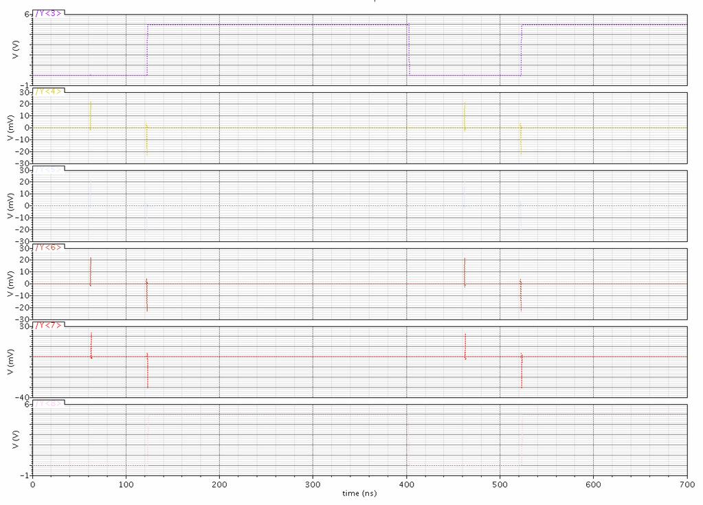


21
22 The spikes that are visible for zero logic output is nothing but the due to the varying transition time and clock skew.
23 1.7. Design Specification and Fabrication details AMI Semiconductor Layer Map C5 This is the layer map for the AMI C5F/N 0.50 micron 3 metal, 2 poly (non-silicided) la rules (AMI_C5F/N), and only for those AMI vendor design rules. For designs that are out using other design rules (or technology-codes), use the standard layer mapping conventions of that design rule set. For submissions in GDS format, the datatype is " (zero) unless specified in the map below. Layer GDS CIF Notes N_WELL 1 A01 ACTIVE 2 A02 N_CHANNEL_FLD 3 A03 Derived from N_WELL when N_CHANNEL_FLD is completely absent from layout. See Note #1 POLY 4 A04 N_PLUS_BLOCK 5 A05 A copy of the drawn P_PLUS_SELECT is used when N_PLUS_BLOCK is completely absent from layout. See Note #1 AMI calls this layer N_PLUS_SELECT and further requires that it be a copy of P_PLUS_SELECT. It is functionally an N_PLUS_BLOCK layer; the drawn regions will not receive the n+ implant. P_PLUS_SELECT 6 A06 CONTACT 8 A08 METAL1 9 A09 VIA1 10 A10 METAL2 11 A11 VIA2 12 A12 METAL3 13 A13 CAP_POLY (POLY2) 26 A26 Optional HRP (HIGH RESISTANCE) 27 A27 THICK_GATE 28 A28 C5F layer N_MINUS_IMPLANT (Npblk) P_MINUS_IMPLANT (Ppblk) 36 A36 C5F layer 37 A37 C5F layer GLASS 14 A14 Note #1: If this layer is present anywhere in the submitted design or anywhere in the
24 design after instantiation, then MOSIS will not derive it. If this layer is not in the submitted design or anywhere in the design after instantiation, then MOSIS will derive that layer from the listed layers. MOSIS does not create a layer partially from a layer drawn by the customer and partially derived from other layers Reading Status Report format from MOSIS Basic Information Design Number This is unique number given for each design by MOSIS on submission of the design. In other words it is you chip identification number. Date Submitted Shows the date when the design was submitted to MOSIS with time stamping Project Status Shows the current status of you chip in fabrication at MOSIS Account Name It is unique college/ individual/ Commercial vendors identification number under whom you send you chip to fabrication i.e its replicates the details of account owner who is registered with MOSIS to send chip for fabrication. Run Date Requested Date when the chip will be sent for fabrication. Usually the date is on the website for each technology Area Reflects the total area of the chip fabricated Checksum On submission o design to MOSIS, MOSIS quickly runs few checksum code to check for any problem in design or layout Design Details Size in X Dimension of the X-co-ordinate of chip Size in Y Dimension of the Y-co-ordinate of chip Wafer Technology Specifies the wafer technology and process detail Fabrication Restricted to Specified on based on what technology the chip will be fabricated Layout Format Format in which design was submitted to MOSIS Top Cell Name Specifies top cell name of you Design Fill MOSIS
25 Bonding Pad Count (Customer) Number of pins in chip user designed Bonding Pad Count (MOSIS) Number of pins MOSIS will package and provide to you Maximum Die Size Specifies maximum die area of the design Layers (Density) Shows details of all the layers used on your design Project Errors Error Shows error on running initial checksum Project Warnings Warning Shows error on running initial checksum Warning Description of error or Warning
26 1.8. Future planning and advancement The design can be easily extended for signed multiplication also this design can be extended to produce much faster result by using pipelining technique which could be extension of this project. Also by mapping the current design to ff.db (Fast fast library cell) the design performance can be further enhanced. Also test logic could be added to the design to have better controllability and observblity.
High speed DCT design using Vedic mathematics N.J.R. Muniraj 1 and N.Senathipathi 2
 464 N.J.R.Muniraj/ Elixir Adv. Engg. Info. 9 (0) 464-468 Available online at www.elixirpublishers.com (Elixir International Journal) Advanced Engineering Informatics Elixir Adv. Engg. Info. 9 (0) 464-468
REALIZATION OF MULTIPLE- OPERAND ADDER-SUBTRACTOR BASED ON VEDIC MATHEMATICS
 REALIZATION OF MULTIPLE- OPERAND ADDER-SUBTRACTOR BASED ON VEDIC MATHEMATICS NEETA PANDEY 1, RAJESHWARI PANDEY 2, SAMIKSHA AGARWAL 3, PRINCE KUMAR 4 Department of Electronics and Communication Engineering
FPGA IMPLEMENTATION OF DFT PROCESSOR USING VEDIC MULTIPLIER. Amrita School of Engineering, Coimbatore, Amrita Vishwa Vidyapeetham, India
 Volume 118 No. 10 2018, 51-56 ISSN: 1311-8080 (printed version); ISSN: 1314-3395 (on-line version) url: http://www.ijpam.eu doi: 10.12732/ijpam.v118i10.7 ijpam.eu FPGA IMPLEMENTATION OF DFT PROCESSOR USING
An Efficient Design of Vedic Multiplier using New Encoding Scheme
 An Efficient Design of Vedic Multiplier using New Encoding Scheme Jai Skand Tripathi P.G Student, United College of Engineering & Research, India Priya Keerti Tripathi P.G Student, Jaypee University of
ASIC Physical Design Top-Level Chip Layout
 ASIC Physical Design Top-Level Chip Layout References: M. Smith, Application Specific Integrated Circuits, Chap. 16 Cadence Virtuoso User Manual Top-level IC design process Typically done before individual
Design of High Speed Area Efficient IEEE754 Floating Point Multiplier
 Design of High Speed Area Efficient IEEE754 Floating Point Multiplier Mownika V. Department of Electronics and Communication Engineering Student*, Narayana Engineering College, Nellore, Andhra Pradesh,
FPGA Programming Technology
 FPGA Programming Technology Static RAM: This Xilinx SRAM configuration cell is constructed from two cross-coupled inverters and uses a standard CMOS process. The configuration cell drives the gates of
Design and Implementation of an Efficient Single Precision Floating Point Multiplier using Vedic Multiplication
 Design and Implementation of an Efficient Single Precision Floating Point Multiplier using Vedic Multiplication Bhavesh Sharma 1, Amit Bakshi 2 bhavesh13121990@gmail.com, abakshi.ece@gmail.com Abstract
CHAPTER 1 INTRODUCTION
 CHAPTER 1 INTRODUCTION Rapid advances in integrated circuit technology have made it possible to fabricate digital circuits with large number of devices on a single chip. The advantages of integrated circuits
Design of Vedic Multiplier for Digital Signal Processing Applications R.Naresh Naik 1, P.Siva Nagendra Reddy 2, K. Madan Mohan 3
 Design of Vedic for Digital Signal Processing Applications R.Naresh Naik 1, P.Siva Nagendra Reddy 2, K. Madan Mohan 3 1 P.G. Scholar (M. Tech), Dept. of ECE, Intell Engineering College, Anantapur 2 P.G.
VHDL IMPLEMENTATION OF FLOATING POINT MULTIPLIER USING VEDIC MATHEMATICS
 VHDL IMPLEMENTATION OF FLOATING POINT MULTIPLIER USING VEDIC MATHEMATICS I.V.VAIBHAV 1, K.V.SAICHARAN 1, B.SRAVANTHI 1, D.SRINIVASULU 2 1 Students of Department of ECE,SACET, Chirala, AP, India 2 Associate
ESE 570 Cadence Lab Assignment 2: Introduction to Spectre, Manual Layout Drawing and Post Layout Simulation (PLS)
") ESE 570 Cadence Lab Assignment 2: Introduction to Spectre, Manual Layout Drawing and Post Layout Simulation (PLS) Objective Part A: To become acquainted with Spectre (or HSpice) by simulating an inverter,
ESE 570 Cadence Lab Assignment 2: Introduction to Spectre, Manual Layout Drawing and Post Layout Simulation (PLS) Objective Part A: To become acquainted with Spectre (or HSpice) by simulating an inverter,
TUTORIAL II ECE 555 / 755 Updated on September 11 th 2006 CADENCE LAYOUT AND PARASITIC EXTRACTION
 TUTORIAL II ECE 555 / 755 Updated on September 11 th 2006 CADENCE LAYOUT AND PARASITIC EXTRACTION After finishing a schematic of your design (Tutorial-I), the next step is creating masks which are for
File: 'ReportV37P-CT89533DanSuo.doc' CMPEN 411, Spring 2013, Homework Project 9 chip, 'Tiny Chip' fabricated through MOSIS program
 MOSIS Chip Test Report Dan Suo File: 'ReportV37P-CT89533DanSuo.doc' CMPEN 411, Spring 2013, Homework Project 9 chip, 'Tiny Chip' fabricated through MOSIS program Technology: 0.5um CMOS, ON Semiconductor
Experiment 9: Binary Arithmetic Circuits. In-Lab Procedure and Report (30 points)
") ELEC 2010 Laboratory Manual Experiment 9 In-Lab Procedure Page 1 of 7 Experiment 9: Binary Arithmetic Circuits In-Lab Procedure and Report (30 points) Before starting the procedure, record the table number
ELEC 2010 Laboratory Manual Experiment 9 In-Lab Procedure Page 1 of 7 Experiment 9: Binary Arithmetic Circuits In-Lab Procedure and Report (30 points) Before starting the procedure, record the table number
Composite Layout CS/EE N-type from the top. N-type Transistor. Diffusion Mask. Polysilicon Mask
 Composite Layout CS/EE 6710 Introduction to Layout Inverter Layout Example Layout Design Rules Drawing the mask layers that will be used by the fabrication folks to make the devices Very different from
The mathematics you have learned about so
 VISUALIZING EXTRAORDINARY WAYS TO MULTIPLY LECTURE 4 The mathematics you have learned about so far has been addition ( adding quantities ); subtraction ( adding negative quantities ); and some ratios and
HOMEWORK 10 CMPEN 411 Due: 4/28/ :30pm
 HOMEWORK 10 CMPEN 411 Due: 4/28/2016 11:30pm Instruction First, fabrication ready the full 8 bit RISC microprocessor chip: redesign the chip (its components) to fit the entire chip fitted into the 40 pin
An Overview of Standard Cell Based Digital VLSI Design
 An Overview of Standard Cell Based Digital VLSI Design With examples taken from the implementation of the 36-core AsAP1 chip and the 1000-core KiloCore chip Zhiyi Yu, Tinoosh Mohsenin, Aaron Stillmaker,
VLSI Test Technology and Reliability (ET4076)
") VLSI Test Technology and Reliability (ET4076) Lecture 8(2) I DDQ Current Testing (Chapter 13) Said Hamdioui Computer Engineering Lab Delft University of Technology 2009-2010 1 Learning aims Describe the
VLSI Test Technology and Reliability (ET4076) Lecture 8(2) I DDQ Current Testing (Chapter 13) Said Hamdioui Computer Engineering Lab Delft University of Technology 2009-2010 1 Learning aims Describe the
VLSI for Multi-Technology Systems (Spring 2003)
") VLSI for Multi-Technology Systems (Spring 2003) Digital Project Due in Lecture Tuesday May 6th Fei Lu Ping Chen Electrical Engineering University of Cincinnati Abstract In this project, we realized the
VLSI for Multi-Technology Systems (Spring 2003) Digital Project Due in Lecture Tuesday May 6th Fei Lu Ping Chen Electrical Engineering University of Cincinnati Abstract In this project, we realized the
Virtuoso Layout Editor
 This tutorial will cover the basic steps involved in using the Cadence layout editor called Virtuoso, extracting layout, and running simulation on the layout. The inverter layout is used as an example
Area-Time Efficient Square Architecture
 AMSE JOURNALS 2015-Series: Advances D; Vol. 20; N 1; pp 21-34 Submitted March 2015; Revised Sept. 21, 2015; Accepted Oct. 15, 2015 Area-Time Efficient Square Architecture *Ranjan Kumar Barik, **Manoranjan
Introduction to 8051 microcontrollers
 Introduction to 8051 microcontrollers Posted on May 7, 2008, by Ibrahim KAMAL, in Micro-controllers, tagged This tutorial is specially tailored to electronics and robotics hobbyists that have already realized
Hardware Design Environments. Dr. Mahdi Abbasi Computer Engineering Department Bu-Ali Sina University
 Hardware Design Environments Dr. Mahdi Abbasi Computer Engineering Department Bu-Ali Sina University Outline Welcome to COE 405 Digital System Design Design Domains and Levels of Abstractions Synthesis
Lab. Course Goals. Topics. What is VLSI design? What is an integrated circuit? VLSI Design Cycle. VLSI Design Automation
 Course Goals Lab Understand key components in VLSI designs Become familiar with design tools (Cadence) Understand design flows Understand behavioral, structural, and physical specifications Be able to
Keywords: throughput, power consumption, area, pipeline, fast adders, vedic multiplier. GJRE-F Classification : FOR Code:
 Global Journal of Researches in Engineering: F Electrical and Electronics Engineering Volume 14 Issue 6 Version 1.0 Type: Double Blind Peer Reviewed International Research Journal Publisher: Global Journals
ProASIC PLUS SSO and Pin Placement Guidelines
 Application Note AC264 ProASIC PLUS SSO and Pin Placement Guidelines Table of Contents Introduction................................................ 1 SSO Data.................................................
ISSN: (Online) Volume 2, Issue 10, October 2014 International Journal of Advance Research in Computer Science and Management Studies
 Volume 2, Issue 10, October 2014 International Journal of Advance Research in Computer Science and Management Studies") ISSN: 2321-7782 (Online) Volume 2, Issue 10, October 2014 International Journal of Advance Research in Computer Science and Management Studies Research Article / Survey Paper / Case Study Available online
ISSN: 2321-7782 (Online) Volume 2, Issue 10, October 2014 International Journal of Advance Research in Computer Science and Management Studies Research Article / Survey Paper / Case Study Available online
FPGA Implementation of Low-Area Floating Point Multiplier Using Vedic Mathematics
 FPGA Implementation of Low-Area Floating Point Multiplier Using Vedic Mathematics R. Sai Siva Teja 1, A. Madhusudhan 2 1 M.Tech Student, 2 Assistant Professor, Dept of ECE, Anurag Group of Institutions
Jan Rabaey Homework # 7 Solutions EECS141
 UNIVERSITY OF CALIFORNIA College of Engineering Department of Electrical Engineering and Computer Sciences Last modified on March 30, 2004 by Gang Zhou (zgang@eecs.berkeley.edu) Jan Rabaey Homework # 7
MICROPROCESSOR RELAY FOR PROTECTION OF ELECTRICAL SYSTEMS
 MICROPROCESSOR RELAY FOR PROTECTION OF ELECTRICAL SYSTEMS V.LALITH KUMAR, IV-EEE S.T.I.C, GARIVIDI, VZM DT. INTRODUCTION: Modern power systems have a high degree of reliability. Power system design together
Chip Card & Security ICs SLE Intelligent 256-Byte EEPROM with Write Protection function and Programmable Security Code
 Chip Card & Security ICs SLE 5542 Intelligent 256-Byte EEPROM with Write Protection function and Programmable Security Code Short Product Information May 2006 Short Product Information Revision History:
NH 67, Karur Trichy Highways, Puliyur C.F, Karur District UNIT-II COMBINATIONAL CIRCUITS
 NH 67, Karur Trichy Highways, Puliyur C.F, 639 114 Karur District DEPARTMENT OF ELETRONICS AND COMMUNICATION ENGINEERING COURSE NOTES SUBJECT: DIGITAL ELECTRONICS CLASS: II YEAR ECE SUBJECT CODE: EC2203
Cadence Virtuoso Schematic Design and Circuit Simulation Tutorial
 Cadence Virtuoso Schematic Design and Circuit Simulation Tutorial Introduction This tutorial is an introduction to schematic capture and circuit simulation for ENGN1600 using Cadence Virtuoso. These courses
Design rule illustrations for the AMI C5N process can be found at:
 Cadence Tutorial B: Layout, DRC, Extraction, and LVS Created for the MSU VLSI program by Professor A. Mason and the AMSaC lab group. Revised by C Young & Waqar A Qureshi -FS08 Document Contents Introduction
Laboratory 6. - Using Encounter for Automatic Place and Route. By Mulong Li, 2013
 CME 342 (VLSI Circuit Design) Laboratory 6 - Using Encounter for Automatic Place and Route By Mulong Li, 2013 Reference: Digital VLSI Chip Design with Cadence and Synopsys CAD Tools, Erik Brunvand Background
VLSI Testing. Lecture Fall 2003
 VLSI Testing Lecture 25 8-322 Fall 23 Announcement Homework 9 is due next Thursday (/2) Exam II is on Tuesday (/8) in class Review Session: When: Next Monday (/7) afternoon, 4pm 6pm Where: B3, HH 2 Outline
Implementation of FFT Processor using Urdhva Tiryakbhyam Sutra of Vedic Mathematics
 Implementation of FFT Processor using Urdhva Tiryakbhyam Sutra of Vedic Mathematics Yojana Jadhav 1, A.P. Hatkar 2 PG Student [VLSI & Embedded system], Dept. of ECE, S.V.I.T Engineering College, Chincholi,
Testing & Verification of Digital Circuits ECE/CS 5745/6745. Hardware Verification using Symbolic Computation
 Testing & Verification of Digital Circuits ECE/CS 5745/6745 Hardware Verification using Symbolic Computation Instructor: Priyank Kalla (kalla@ece.utah.edu) 3 Credits Mon, Wed 1:25-2:45pm, WEB 2250 Office
An Efficient Elliptic Curve Cryptography Arithmetic Using Nikhilam Multiplication
 The International Journal Of Engineering And Science (IJES) Volume 4 Issue 4 Pages PP.45-50 2015 ISSN (e): 2319 1813 ISSN (p): 2319 1805 An Efficient Elliptic Curve Cryptography Arithmetic Using Nikhilam
EECS 627, Lab Assignment 2
 EECS 627, Lab Assignment 2 1 Introduction In this lab assignment, you will extend the process of designing your multiplier chip. You will add two more blocks (a pseudo-random test pattern generator and
Instruction on padframe
 Instruction on padframe The padframe is a 40-pins padframe for the AMI ABN 1.6um process from MOSIS located at http://www.mosis.org/cell-libraries/scn16-pads/. You should download the CIF file from the
Hardware Modeling using Verilog Prof. Indranil Sengupta Department of Computer Science and Engineering Indian Institute of Technology, Kharagpur
 Hardware Modeling using Verilog Prof. Indranil Sengupta Department of Computer Science and Engineering Indian Institute of Technology, Kharagpur Lecture 01 Introduction Welcome to the course on Hardware
Unit 6 1.Random Access Memory (RAM) Chapter 3 Combinational Logic Design 2.Programmable Logic
 Chapter 3 Combinational Logic Design 2.Programmable Logic") EE 200: Digital Logic Circuit Design Dr Radwan E Abdel-Aal, COE Unit 6.Random Access Memory (RAM) Chapter 3 Combinational Logic Design 2. Logic Logic and Computer Design Fundamentals Part Implementation
EE 200: Digital Logic Circuit Design Dr Radwan E Abdel-Aal, COE Unit 6.Random Access Memory (RAM) Chapter 3 Combinational Logic Design 2. Logic Logic and Computer Design Fundamentals Part Implementation
Spiral 2-8. Cell Layout
 2-8.1 Spiral 2-8 Cell Layout 2-8.2 Learning Outcomes I understand how a digital circuit is composed of layers of materials forming transistors and wires I understand how each layer is expressed as geometric
Digital Circuit Design and Language. Datapath Design. Chang, Ik Joon Kyunghee University
 Digital Circuit Design and Language Datapath Design Chang, Ik Joon Kyunghee University Typical Synchronous Design + Control Section : Finite State Machine + Data Section: Adder, Multiplier, Shift Register
Date Performed: Marks Obtained: /10. Group Members (ID):. Experiment # 09 MULTIPLEXERS
:. Experiment # 09 MULTIPLEXERS") Name: Instructor: Engr. Date Performed: Marks Obtained: /10 Group Members (ID):. Checked By: Date: Experiment # 09 MULTIPLEXERS OBJECTIVES: To experimentally verify the proper operation of a multiplexer.
Name: Instructor: Engr. Date Performed: Marks Obtained: /10 Group Members (ID):. Checked By: Date: Experiment # 09 MULTIPLEXERS OBJECTIVES: To experimentally verify the proper operation of a multiplexer.
 An Overview of Microprocessor The first question comes in a mind "What is a microprocessor?. Let us start with a more familiar term computer. A digital computer is an electronic machine capable of quickly
CALIFORNIA INSTITUTE OF TECHNOLOGY VIBA Correlator Project. VLSI TECHNOLOGY REPORT M. S. Ewing December 28, 1984
 VLBA CORRELATOR MEMO VC 036 ********************* CALIFORNIA INSTITUTE OF TECHNOLOGY VIBA Correlator Project VLSI TECHNOLOGY REPORT M. S. Ewing December 28, 1984 I. INTRODUCTION. The VIBA correlator must
DLD VIDYA SAGAR P. potharajuvidyasagar.wordpress.com. Vignana Bharathi Institute of Technology UNIT 1 DLD P VIDYA SAGAR
 UNIT I Digital Systems: Binary Numbers, Octal, Hexa Decimal and other base numbers, Number base conversions, complements, signed binary numbers, Floating point number representation, binary codes, error
Chapter 8 Summary: The 8086 Microprocessor and its Memory and Input/Output Interface
 Chapter 8 Summary: The 8086 Microprocessor and its Memory and Input/Output Interface Figure 1-5 Intel Corporation s 8086 Microprocessor. The 8086, announced in 1978, was the first 16-bit microprocessor
CPE/EE 427, CPE 527, VLSI Design I: Tutorial #3, Standard cell design flow (from schematic to layout, 8-bit accumulator)
") CPE/EE 427, CPE 527, VLSI Design I: Tutorial #3, Standard cell design flow (from schematic to layout, 8-bit accumulator) Joel Wilder, Aleksandar Milenkovic, ECE Dept., The University of Alabama in Huntsville
CPE/EE 427, CPE 527, VLSI Design I: Tutorial #3, Standard cell design flow (from schematic to layout, 8-bit accumulator) Joel Wilder, Aleksandar Milenkovic, ECE Dept., The University of Alabama in Huntsville
Chip Card & Security ICs SLE Intelligent 1024 Byte EEPROM with Write Protection and Programmable Security Code
 Chip Card & Security ICs SLE 5528 Intelligent 1024 Byte EEPROM with Write Protection and Programmable Security Code Short Product Information May 2007 Short Product Information Revision History: Current
CMOS VLSI Design Lab 4: Full Chip Assembly
 CMOS VLSI Design Lab 4: Full Chip Assembly In this final lab, you will assemble and simulate your entire MIPS microprocessor! You will build your top level chip cell by connecting the datapath, aludec,
An overview of standard cell based digital VLSI design
 An overview of standard cell based digital VLSI design Implementation of the first generation AsAP processor Zhiyi Yu and Tinoosh Mohsenin VCL Laboratory UC Davis Outline Overview of standard cellbased
Problem Formulation. Specialized algorithms are required for clock (and power nets) due to strict specifications for routing such nets.
 due to strict specifications for routing such nets.") Clock Routing Problem Formulation Specialized algorithms are required for clock (and power nets) due to strict specifications for routing such nets. Better to develop specialized routers for these nets.
Clock Routing Problem Formulation Specialized algorithms are required for clock (and power nets) due to strict specifications for routing such nets. Better to develop specialized routers for these nets.
Area Efficient, Low Power Array Multiplier for Signed and Unsigned Number. Chapter 3
 Area Efficient, Low Power Array Multiplier for Signed and Unsigned Number Chapter 3 Area Efficient, Low Power Array Multiplier for Signed and Unsigned Number Chapter 3 3.1 Introduction The various sections
Addition and multiplication
 Addition and multiplication Arithmetic is the most basic thing you can do with a computer, but it s not as easy as you might expect! These next few lectures focus on addition, subtraction, multiplication
UNIT IV CMOS TESTING
 UNIT IV CMOS TESTING 1. Mention the levels at which testing of a chip can be done? At the wafer level At the packaged-chip level At the board level At the system level In the field 2. What is meant by
Hardware Design with VHDL PLDs IV ECE 443
 Embedded Processor Cores (Hard and Soft) Electronic design can be realized in hardware (logic gates/registers) or software (instructions executed on a microprocessor). The trade-off is determined by how
Layout and Layout Verification. of an Inverter Circuit
 Layout and Layout Verification of an Inverter Circuit Santa Clara University Department of Electrical Engineering By Piyush Panwar Under Guidance of Dr Samiha Mourad Date of Last Revision: August 7, 2010
TEXAS INSTRUMENTS ANALOG UNIVERSITY PROGRAM DESIGN CONTEST MIXED SIGNAL TEST INTERFACE CHRISTOPHER EDMONDS, DANIEL KEESE, RICHARD PRZYBYLA SCHOOL OF
 TEXASINSTRUMENTSANALOGUNIVERSITYPROGRAMDESIGNCONTEST MIXED SIGNALTESTINTERFACE CHRISTOPHEREDMONDS,DANIELKEESE,RICHARDPRZYBYLA SCHOOLOFELECTRICALENGINEERINGANDCOMPUTERSCIENCE OREGONSTATEUNIVERSITY I. PROJECT
Design Guidelines for Optimal Results in High-Density FPGAs
 White Paper Introduction Design Guidelines for Optimal Results in High-Density FPGAs Today s FPGA applications are approaching the complexity and performance requirements of ASICs. In some cases, FPGAs
O PT I C Alan N. Willson, Jr. AD-A ppiov' 9!lj" 2' 2 1,3 9. Quarterly Progress Report. (October 1, 1992 through December 31, 1992)
") AD-A260 754 Quarterly Progress Report (October 1, 1992 through December 31, 1992) O PT I C on " 041 o 993 VLSI for High-Speed Digital Signal Processing prepared for Accesion For NTIS CRA&I Office of Naval
AD-A260 754 Quarterly Progress Report (October 1, 1992 through December 31, 1992) O PT I C on " 041 o 993 VLSI for High-Speed Digital Signal Processing prepared for Accesion For NTIS CRA&I Office of Naval
Squaring using Vedic mathematics and its architectures: a survey
 www.ijiarec.com ISSN:2348-2079 Volume-6 Issue-1 International Journal of Intellectual Advancements and Research in Engineering Computations Squaring using Vedic mathematics and its architectures: a survey
ENEE245 Digital Circuits and Systems Lab Manual
 ENEE245 Digital Circuits and Systems Lab Manual Department of Engineering, Physical & Computer Sciences Montgomery College Version 1.1 Copyright Prof. Lan Xiang (Do not distribute without permission) 1
Verilog Implementation of High Performance RC6 Algorithm using Ancient Indian Vedic Mathematics
 www.semargroups.org, www.ijsetr.com ISSN 2319-8885 Vol.02,Issue.17, November-2013, Pages:1994-2002 Verilog Implementation of High Performance RC6 Algorithm using Ancient Indian Vedic Mathematics D. RAJESH
Computer Arithmetic Multiplication & Shift Chapter 3.4 EEC170 FQ 2005
 Computer Arithmetic Multiplication & Shift Chapter 3.4 EEC170 FQ 200 Multiply We will start with unsigned multiply and contrast how humans and computers multiply Layout 8-bit 8 Pipelined Multiplier 1 2
Elec 326: Digital Logic Design
 Elec 326: Digital Logic Design Project Requirements Fall 2005 For this project you will design and test a three-digit binary-coded-decimal (BCD) adder capable of adding positive and negative BCD numbers.
The Procedure for Laying out the inverter in TSMC s 0.35 micron Technogy using MOSIS SCMOS SCN4M_SUBM design rules.
 Page 1 of 5 CADENCE TUTORIAL Creating Layout of an inverter: click on File->library->new a Create Library form appears, fill it as follows: in the name field enter: inverter select "Attach to existing
ENEE245 Digital Circuits and Systems Lab Manual
 ENEE245 Digital Circuits and Systems Lab Manual Department of Engineering, Physical & Computer Sciences Montgomery College Modified Fall 2017 Copyright Prof. Lan Xiang (Do not distribute without permission)
Finite State Machines (FSMs) and RAMs and CPUs. COS 116, Spring 2011 Sanjeev Arora
 and RAMs and CPUs. COS 116, Spring 2011 Sanjeev Arora") Finite State Machines (FSMs) and RAMs and CPUs COS 116, Spring 2011 Sanjeev Arora Recap Combinational logic circuits: no cycles, hence no memory Sequential circuits: cycles allowed; can have memory as
Finite State Machines (FSMs) and RAMs and CPUs COS 116, Spring 2011 Sanjeev Arora Recap Combinational logic circuits: no cycles, hence no memory Sequential circuits: cycles allowed; can have memory as
Overview. EECS Components and Design Techniques for Digital Systems. Lec 16 Arithmetic II (Multiplication) Computer Number Systems.
 Computer Number Systems.") Overview EE 15 - omponents and Design Techniques for Digital ystems Lec 16 Arithmetic II (Multiplication) Review of Addition Overflow Multiplication Further adder optimizations for multiplication LA in
Overview EE 15 - omponents and Design Techniques for Digital ystems Lec 16 Arithmetic II (Multiplication) Review of Addition Overflow Multiplication Further adder optimizations for multiplication LA in
CSCB58 - Lab 3. Prelab /3 Part I (in-lab) /2 Part II (in-lab) /2 TOTAL /8
 /2 Part II (in-lab) /2 TOTAL /8") CSCB58 - Lab 3 Latches, Flip-flops, and Registers Learning Objectives The purpose of this exercise is to investigate the fundamental synchronous logic elements: latches, flip-flops, and registers. Prelab
CSCB58 - Lab 3 Latches, Flip-flops, and Registers Learning Objectives The purpose of this exercise is to investigate the fundamental synchronous logic elements: latches, flip-flops, and registers. Prelab
MOSIS Scalable CMOS (SCMOS) Design Rules
 Design Rules") MOSIS Scalable CMOS (SCMOS) Design Rules (Revision 8.00) From : http://www.mosis.com/technical/designrules/scmos/scmos-main.html Updated: October 4, 2004 1. Introduction This document defines the official
MOSIS Scalable CMOS (SCMOS) Design Rules (Revision 8.00) From : http://www.mosis.com/technical/designrules/scmos/scmos-main.html Updated: October 4, 2004 1. Introduction This document defines the official
CHAPTER 7 FPGA IMPLEMENTATION OF HIGH SPEED ARITHMETIC CIRCUIT FOR FACTORIAL CALCULATION
 86 CHAPTER 7 FPGA IMPLEMENTATION OF HIGH SPEED ARITHMETIC CIRCUIT FOR FACTORIAL CALCULATION 7.1 INTRODUCTION Factorial calculation is important in ALUs and MAC designed for general and special purpose
HOMEWORK 9 CMPEN 411 Due: 4/12/ :30pm
 HOMEWORK 9 CMPEN 411 Due: 4/12/2016 11:30pm Learning Objective Complete the full 8 bit RISC microprocessor chip design by placing the processor core design into the 40 pin 'tiny' chip pad frame. Do verify
TSEA44 - Design for FPGAs
 2015-11-24 Now for something else... Adapting designs to FPGAs Why? Clock frequency Area Power Target FPGA architecture: Xilinx FPGAs with 4 input LUTs (such as Virtex-II) Determining the maximum frequency
FPGA Power Management and Modeling Techniques
 FPGA Power Management and Modeling Techniques WP-01044-2.0 White Paper This white paper discusses the major challenges associated with accurately predicting power consumption in FPGAs, namely, obtaining
DIGITAL SYSTEM DESIGN
 DIGITAL SYSTEM DESIGN Prepared By: Engr. Yousaf Hameed Lab Engineer BASIC ELECTRICAL & DIGITAL SYSTEMS LAB DEPARTMENT OF ELECTRICAL ENGINEERING Digital System Design 1 Name: Registration No: Roll No: Semester:
Verilog for High Performance
 Verilog for High Performance Course Description This course provides all necessary theoretical and practical know-how to write synthesizable HDL code through Verilog standard language. The course goes
Design of Arithmetic circuits
 Design of Arithmetic circuits ic principle of pipelining ditional approach Input Data clk Process < 100 ns Through 10 MH elining approach Throughput considerably. increases Chip area also increases. Latency
NH 67, Karur Trichy Highways, Puliyur C.F, Karur District DEPARTMENT OF INFORMATION TECHNOLOGY CS 2202 DIGITAL PRINCIPLES AND SYSTEM DESIGN
 NH 67, Karur Trichy Highways, Puliyur C.F, 639 114 Karur District DEPARTMENT OF INFORMATION TECHNOLOGY CS 2202 DIGITAL PRINCIPLES AND SYSTEM DESIGN UNIT 2 COMBINATIONAL LOGIC Combinational circuits Analysis
ECE 375: Computer Organization and Assembly Language Programming
 ECE 375: Computer Organization and Assembly Language Programming SECTION OVERVIEW Lab 5 Large Number Arithmetic Complete the following objectives: ˆ Understand and use arithmetic/alu instructions. ˆ Manipulate
CIS-331 Fall 2014 Exam 1 Name: Total of 109 Points Version 1
 Version 1 1. (24 Points) Show the routing tables for routers A, B, C, and D. Make sure you account for traffic to the Internet. Router A Router B Router C Router D Network Next Hop Next Hop Next Hop Next
CMOS VLSI Design. Final Project
 Harris CMOS VLSI Design Final Project 1. Overview The final project is a chance for you to apply your new skills in VLSI design to a moderate sized problem of your choosing as part of a two-person team.
Data Representation Type of Data Representation Integers Bits Unsigned 2 s Comp Excess 7 Excess 8
 Data Representation At its most basic level, all digital information must reduce to 0s and 1s, which can be discussed as binary, octal, or hex data. There s no practical limit on how it can be interpreted
The Microprocessor as a Microcosm:
 The Microprocessor as a Microcosm: A Hands-On Approach to VLSI Design Education David Harris David_Harris@hmc.edu November 2002 Harvey Mudd College Claremont, CA Outline Introduction Course Organization
Overview. Design flow. Principles of logic synthesis. Logic Synthesis with the common tools. Conclusions
 Logic Synthesis Overview Design flow Principles of logic synthesis Logic Synthesis with the common tools Conclusions 2 System Design Flow Electronic System Level (ESL) flow System C TLM, Verification,
Compact Integrated Processor
 Compact Integrated Processor EE498 Report Senior Design II Jared Hayes Nick Repetti Jason Silic Faculty Advisor: Dr. R. Jacob Baker 12 May 2015 1 Table of Contents 1. Introduction......3 1.1. Introduction......3
VALLIAMMAI ENGINEERING COLLEGE. SRM Nagar, Kattankulathur DEPARTMENT OF ELECTRONICS AND COMMUNICATION ENGINEERING EC6302 DIGITAL ELECTRONICS
 VALLIAMMAI ENGINEERING COLLEGE SRM Nagar, Kattankulathur-603 203 DEPARTMENT OF ELECTRONICS AND COMMUNICATION ENGINEERING EC6302 DIGITAL ELECTRONICS YEAR / SEMESTER: II / III ACADEMIC YEAR: 2015-2016 (ODD
Menu. word size # of words byte = 8 bits
 Menu LSI Components >Random Access Memory (RAM) Static RAM (SRAM) Dynamic RAM (DRAM) Read-Only Memory (ROM) Look into my... See figures from Lam text on web: RAM_ROM_ch6.pdf 1 It can be thought of as 1
ProASIC3/E SSO and Pin Placement Guidelines
 ProASIC3/E SSO and Pin Placement Guidelines Introduction SSO Effects Ground bounce and VCC bounce have always been present in digital integrated circuits (ICs). With the advance of technology and shrinking
ECE 353 Lab 4. Verilog Review. Professor Daniel Holcomb UMass Amherst Fall 2017
 ECE 353 Lab 4 Verilog Review Professor Daniel Holcomb UMass Amherst Fall 2017 What You Will Do In Lab 4 Design and implement a serial MIDI receiver Hardware in an Altera Complex Programmable Logic Device
[Sahu* et al., 5(7): July, 2016] ISSN: IC Value: 3.00 Impact Factor: 4.116
![[Sahu* et al., 5(7): July, 2016] ISSN: IC Value: 3.00 Impact Factor: 4.116](/thumbs/86/94398605.jpg "[Sahu* et al., 5(7): July, 2016] ISSN: IC Value: 3.00 Impact Factor: 4.116") IJESRT INTERNATIONAL JOURNAL OF ENGINEERING SCIENCES & RESEARCH TECHNOLOGY SPAA AWARE ERROR TOLERANT 32 BIT ARITHMETIC AND LOGICAL UNIT FOR GRAPHICS PROCESSOR UNIT Kaushal Kumar Sahu*, Nitin Jain Department
IJESRT INTERNATIONAL JOURNAL OF ENGINEERING SCIENCES & RESEARCH TECHNOLOGY SPAA AWARE ERROR TOLERANT 32 BIT ARITHMETIC AND LOGICAL UNIT FOR GRAPHICS PROCESSOR UNIT Kaushal Kumar Sahu*, Nitin Jain Department
Process technology and introduction to physical
 Neuromorphic Engineering II Lab 3, Spring 2014 1 Lab 3 March 10, 2014 Process technology and introduction to physical layout Today you will start to learn to use the Virtuoso layout editor XL which is
Testing Principle Verification Testing
 ECE 553: TESTING AND TESTABLE DESIGN OF DIGITAL SYSTES Test Process and Test Equipment Overview Objective Types of testing Verification testing Characterization testing Manufacturing testing Acceptance
EECE 285 VLSI Design. Cadence Tutorial EECE 285 VLSI. By: Kevin Dick Co-author: Jeff Kauppila Co-author: Dr. Arthur Witulski
 Cadence Tutorial EECE 285 VLSI By: Kevin Dick Co-author: Jeff Kauppila Co-author: Dr. Arthur Witulski 1 Table of Contents Purpose of Cadence 1) The Purpose of Cadence pg. 4 Linux 1) The Purpose of Linux
Agenda EE 224: INTRODUCTION TO DIGITAL CIRCUITS & COMPUTER DESIGN. Lecture 1: Introduction. Go over the syllabus 3/31/2010
 // EE : INTRODUCTION TO DIGITAL CIRCUITS & COMPUTER DESIGN Lecture : Introduction /9/ Avinash Kodi, kodi@ohio.edu Agenda Go over the syllabus Introduction ti to Digital it Systems // Why Digital Systems?