Compact Integrated Processor
|
|
|
- Lenard Webb
- 5 years ago
- Views:
Transcription
1 Compact Integrated Processor EE498 Report Senior Design II Jared Hayes Nick Repetti Jason Silic Faculty Advisor: Dr. R. Jacob Baker 12 May
2 Table of Contents 1. Introduction Introduction System Overview Instruction Set Instruction Description Instruction Encoding Examples System Architecture Functional Analysis and Requirements Trade offs SRAM Design and Implementation Precharging Circuit Write Circuit Design Control Unit Overview Control Signal List Control Signal Block Diagram Register File Design and Implementation Alternatives and Trade Offs ALU Design and Implementation Simulations Project Results Prototype Cost Estimate Cost Estimate.27 Appendix A...28 A.1. Control Signal Generation For All Instructions, simulation of entire chip 2
3 1. Introduction 1.1 Introduction MIPS (Microprocessor without Interlocked Pipeline Stages) is a popular implementation of a reduced instruction set computer (RISC). MIPS architectures are typically 32 bit, but 64 bit versions have been developed in more recent years. It became a widely used processor for embedded systems design and has been implemented in many consumer electronics products. These included routers, devices that ran Windows CE, and Sony video game consoles. Due to its popularity in modern electronics in the 1990 s, it has often been studied in computer architecture courses. It is an effective, yet simple processor that fulfills the features required in a modern processor but without too much unnecessary complexity. Our Senior Design project is a simple 8 bit CPU with onboard SRAM memory. Our instruction set is loosely based on the MIPS architecture with some significant simplifications. For example, our architecture only supports 21 simple instructions and instruction size has been reduced to two bytes. The 512 bytes of on die memory is used to store both instructions and data. The purpose of this project is twofold. Our first objective is to demonstrate the utility of our design. Most microprocessors of this size (the chip only has about 35,000 transistors) will use an external memory chip to store their program. The onboard memory used here results in a more compact design. The second goal is to document our design to provide an example for future students. Since our processor will be much easier to interpret and apply than most modern microprocessors, students can use it to create simple projects as an entry into embedded systems. 2. System Overview 2.1 Instruction Set Our processor uses a modified instruction set with 16 bits per instruction, instead of the typical 32 bit instruction set. This system was chosen because our onboard SRAM is only 512 bytes, so conserving memory is very important. Also, the large instruction size is mostly to accommodate large register files (32 registers is typical) and large memory spaces. We only need nine bits to specify a memory location, so even our jump instructions can store the opcode (4 bits), register to compare (3 bits) and absolute address (9 bits) for a total of 16 bits. There was really no need for a larger instruction size which would have just increased the complexity of our design. The first thing that should be understood is the various instruction formats. In the below diagrams, the number represent the bit at the end of the field. For example, the opcode is the four most significant bits. In a two byte instruction bit are numbered from 0 (LSB) to 15 (MSB). The opcode 3
4 therefore has bits numbered from 12 to 15. The text in bold indicates the name of the field, such as opcode or L6 (a literal value). Arithmetic Instruction 15 opcode r0 9 8 r1 6 5 r2 3 2 flags 0 Arithmetic Instruction with Literal (L6) 15 opcode r0 9 8 L6 3 2 flags 0 Control Instruction 15 opcode r0 9 8 L9 0 Data Instruction (bit 8 is unused) 15 opcode r L8 0 Shift Instruction 15 opcode r0 9 8 r1 6 5 unused 3 2 L3 0 The instructions are fetched in two separate read. There are 21 instructions accessed through a 4 bit opcode and 3 bit flag field on arithmetic and IO instructions. For example, opcode 0000 is an arithmetic instruction, with the particular instruction (ADD, SUB, XOR, etc.) determined by the bits in the Flags field. The encoding for the various instructions is as follows: 4
5 Table 1 opcode instruction opcode instruction 0000 ARITH 1000 JNE 0001 LOAD 1001 JGE 0010 SHL 1010 [not used] 0011 SET 1011 NOP 0100 IO 1100 JE 0101 STORE 1101 JG 0110 SHR 1110 ROR 0111 STOP 1111 STOP* *Note that the STOP instruction has two opcodes used for it. The ARITH instruction breaks down as follows, depending on the Flags field flags instruction flags instruction 000 ADDI 100 AND 001 ADD 101 NOT 010 SUB 110 XOR 011 OR 111 [not used] The IO instructions depend on the least significant bit of the Flags field. If it is 0, the instruction is IN, otherwise the instruction is OUT Instruction Description The basic operation of the instructions is described here. The following section will describe how the various fields in the 16 bit instruction are used. The instructions are presented below with this format: r0, r1, r2 are 3 bit fields that specify one of eight registers. L9 is a nine bit literal used to specify a jump address. L6 is a six bit literal used for the ADDI instruction. L8 is an eight bit literal used for setting a register to a value L3 is a three bit literal to control the amount of shifting or rotation for SHL, SHR, and ROR instructions. Finally, note that for instructions with unused fields (e.g., the STOP instruction only uses the opcode and has twelve bits unused) these bits are don t care bits. They can be filled with any sequence of ones and zeros and the CPU will not care. They are usually padded with zeros, but this is not required. 5
6 Table 2: Instruction Description Instruction Encoding Format Notes ADD r0, r1, r2 Arithmetic Instruction r0 gets the result of r1 + r2 ADDI r0, L6 Arithmetic Instruction with Literal r0 gets the result of r0 + L6 (sign extended) SUB r0, r1, r2 Arithmetic Instruction r0 = r1 r2 OR r0, r1, r2 Arithmetic Instruction r0 = r1 r2 (bitwise OR operation) AND r0, r1, r2 Arithmetic Instruction r0 = r1 & r2 (bitwise AND operation) NOT r0, r1 Arithmetic Instruction r0 = ~r1 (bitwise inversion) XOR r0, r1, r2 Arithmetic Instruction r0 = r1 ^ r2 (bitwise XOR operation) IN r0 Arithmetic Instruction r0 get the value placed on the IO input pins OUT r0 Arithmetic Instruction The value in r0 is placed into the output register, and appears on the output IO pins JE r0, L9 Control Instruction Jump to address L9 if r0 is equal to zero. JNE r0, L9 Control Instruction Jump to address L9 if r0 is not equal to zero. JG r0, L9 Control Instruction Jump to address L9 if r0 is greater than zero (signed comparison) JGE r0, L9 Control Instruction Jump to address L9 if r0 is greater than or equal to zero (also signed) LOAD r0, L9 Control Instruction Load data at address L9 into register r0 STORE r0, L9 Control Instruction Store contents of register r0 at address L9 SET r0, L8 Data Instruction Store the value L8 into register r0 STOP Any Stop the execution of the current program, until a reset signal. Only the opcode is used for STOP and NOP instructions. The other twelve bits are unused. NOP Any No operation 6
7 SHL r0, r1, L3 Shift Instruction Shift register r1 left by L3, store result in r0. [Shift in zeros] SHR r0, r1, L3 Shift Instruction Shift register r1 right by L3, store result in r0. [Shift in zeros] ROR r0, r1, L3 Shift Instruction Rotate the bits in r1 to the right by L3 positions, store in r Instruction Encoding Examples The above tables and lists may be a bit confusing, so the following examples will hopefully clear up any confusion. The complete process of forming an instruction is considered and explained, step by step. Example 1 SHR R4, R3, #6 Here R4 indicates register four (don t confuse with the register fields above such as r0, r1, and r2). R3 indicates register 3 and #6 is a literal value. The value in register 3 is shifted right six positions and the result is stored in R4. From Table 1 above we discover that the opcode for SHR is 0x6. The first field is 0x4 and the first bit of field r1 is 0. The upper eight bits of this instruction is therefore 0x68, or 104 in decimal. The first two bits of the lower byte are 11, from register three. The next three bits we leave as zeros because they are unused. The last three bits are 011, which is our literal 6. The lower byte is therefore 0xC6, which is 198 in decimal. The complete instruction is therefore 0x68C6. If you were writing a program on an Arduino like we did to load the SRAM, the first byte loaded is the lower byte, so your data array would be like this, excluding the other instructions: int data[16] = {..,.., 198, 104,..,..,.}; Example 2 ADDI R7, #62 7
8 Note that this instruction subtracts two from R7 and stores the result back in R7. Remember that the literal for this instruction is sign extended, so 62 is binary , which is two s complement for negative two. Table 1 shows the opcode is 0x0. Table 2 tells us to use the Arithmetic Instruction with Literal format. Field r0 is 111 (R7) and the literal L6 is Finally, the flags field should be 000 for the ADDI instruction. The upper byte is therefore 0x0F, or decimal 15. The lower byte is 0xF0, which is 240. Example 3 OUT R2 The complete instruction is 0x0FF0, which is loaded into memory as 240, 15 (lower byte first!). This is an IO instruction with opcode 0x4. The Arithmetic Instruction format is used, but only the first register field is used. The flags field has to be 001 for the OUT instruction and 000 for the IN instruction. The upper byte is therefore 0x44 = 68. The lower byte is 0x01 = decimal 1. Example 4 JG R3, #420 The complete instruction is 0x4401, which is stored into memory as 1, 68. The opcode for JG is 0xD. The register field is 011. The address #420 is in binary. The upper byte is therefore 0xD7 which is 215. The lower byte is 0xA4 which is 164 in decimal. The complete instruction is 0xD7A4, or the decimal numbers 164, 215. Note that the jump and control instructions use a fixed 9 bit address as their target. However, it is very easy to use the STORE instruction to write another value to the lower eight bits of this address. This feature can be used to implement subroutines. Simply write the return address to the address of a jump instruction at the end of the subroutine. When the program execution reaches this point it will simply return to the location from which it was called (assuming you wrote the correct return address). 2.2 System Architecture The main components of the MIPS processor include: Control Unit SRAM ALU Register File 8
9 Control Unit This processor is essentially a massive state machine. Neglecting the SRAM for a moment, the CPU s state is completely defined by the contents of the register file, ALU registers, and control unit registers. The next state is a deterministic result of the current state, and is achieved by the use of only twenty four control signals. These control signals are generated by combinational logic which has a delay less than one half of a clock cycle. Some of these control signals are for the internal use of the Control Unit (CU). For example, the StepReset signal will reset the step counter, which tracks the current instruction s stage of execution. Other signals are for the ALU arithmetic logic, such as the three ALU control signals. The control unit does have some additional responsibilities for the shifting instructions. The barrel shifter in the ALU can only shift data one bit position per clock cycle. To implement longer shifts, a small three bit counter is necessary. SRAM The SRAM is of a standard six transistor (6T) design. A simple precharge is applied to the bitlines when the clock signal is high to prevent a low voltage bitline from flipping the datum stored in a cell. Loading data into the SRAM is accomplished by a specialized circuit that aids in the sequential writing of data to the SRAM. Arithmetic Logic Unit (ALU) The Arithmetic Logic Unit is responsible for all of the Arithmetic and Logic functions that most of the operations rely on. The ALU can perform multiple operations which will be discussed in a later section. Data is clocked into Registers A and B from their respective buses and the appropriate action is performed based on the input signals from the Control Unit. The ALU also handles the calculations for the jump instructions. Register File (RF) The register file is responsible for storing data in registers specified by the instruction register for use by the ALU. Since this is an 8 bit processor it reads in 3 bit opcodes and decodes them into the clocks of each register. This register file can read two registers and write to a single register at once. Two 3 to 8 decoders help to drive multiplexing for each of the two buses leading out of it. The bus A decoder is also responsible for gating the clock of the registers to select which register to write to. Instead of using multiplexers to determine which registers to output to the buses, 8 bit transmission gates powered by the decoders are used for each register. There are two sets of the 8 bit transmission gates in total, one for each bus. We present a top level schematic with the various parts of the processor labeled on the next page. Note the precharge circuit used to always define the voltage on BusA. This is important because when all the tri state buffers are in the Hi Z state, the voltage on the bus could float, possibly leading to contention 9
10 current in inverters connected to the bus. This could lead to failure of the chip, or fluctuations in the power supply voltage. 2.3 Functional Analysis and Requirements Our processor is designed and simulated using Cadence Virtuoso design software with Spectre and Ultrasim simulation plugins. The processor was designed from scratch on the transistor level and fabricated on a chip using the MOSIS On Semiconductor 500 nm rules and the C5 CMOS process, which contains 2 polysilicon layers and 3 metal layers. Therefore, all digital logic and components will be custom made in order to fit the specifications of our project and the MOSIS design rules. Cadence allows us to design the chip layout according to those rules and will make checks to ensure that our layout stays consistent with them. The fabrication process takes considerable time and resources; therefore, we must ensure that our design is properly simulated so that our fabricated chip works as intended in our design. We use Spectre and Ultrasim to simulate the schematics of all of our components to ensure proper operation. Then, Cadence checks that our layouts exactly match the schematics in order to adhere to our simulation results. 2.4 Trade offs We had to consider many trade offs in order to simplify our processor to fit our time constraints and resources. Designing an 8 bit processor instead of a 32 bit processor obviously reduces the chip s processing power and capabilities. Using a two byte instruction length allows the user to have a simpler and more streamlined set of instructions, but at the cost of flexibility. We also chose to forego implementing a pipelined microarchitecture. A pipelined architecture would have improved our processor s execution time enormously; however, the added design complexity would not have been feasible to implement in our project, considering our time limitations. So, we implemented a multi cycle architecture instead. We chose to include on board memory in our processor. This eliminates many additional off chip components, such as an external memory chips. Unfortunately, the SRAM memory is volatile and loses its data after losing power. The programs must therefore be loaded onto the chip again every time the power is turned on again. This is a severe problem for the commercialization of this design. Our process technology can not be used to fabricate flash memory cells or other non volatile forms of storage. 3. SRAM 3.1 SRAM Design and implementation The basic SRAM cell stores one bit of information. Our design is the quite common 6T (six transistors) cell. Although a four transistor cell exists, the resistors it used are difficult to fabricate in a small space and contribute to static power dissipation. The basic schematic is presented below, consisting of two cross coupled inverters and two NMOS access transistors. 10
11 Writing data to the cell is accomplished by overpowering the internal transistors to flip the bit. Only writing a low voltage (actually 0V) will work, because the NMOS pass gate passes a logic 0 better and the PMOS transistor is easier to overpower. Therefore, a low voltage on the A bitline writes a zero to the cell, and a low voltage on the Ai bitline writes a logic one into the cell. Below is the layout of the SRAM cell, with prominent features illustrated. The bitlines run vertically on Metal3, while the row select and byte select signals run horizontally on Metal2. 11

12 3.2 Precharging circuit The original plan did not include provision for precharging the bitlines. While this would have simplified the design, simulations revealed that a bitline at ground potential could actually write data into another cell when the select line for that cell was asserted. The solution involves precharging the bitlines to a high enough voltage to avoid this problem. Although charging the bitlines to VDD V thn through an NMOS transistor could have worked, I decided to do a more complicated three transistor design to get a more precise voltage. The stable output voltage of the below circuit is about 3.24V, with a 10MEG load to ground. The long length transistors limit the current that can flow, making sure the maximum sustained current is less than 100uA/via. When the input is low, the PMOS transistors turn on and move the voltage on the output line toward 3.2V. 12
13 3.3 Write Driver circuit When data is loaded into the SRAM, the data comes from an external source. In addition, data is loaded into sequential memory locations, starting at 0x000. Therefore, the address bus is connected to a nine bit upcounter, and the write bus is connected to the external input. The external procedure for writing data to the SRAM is simple. Assert the Load Write Enable signal, and send a reset signal (Reset is active low) to reset the address counter. The values on the 8 input lines will be written to the SRAM on active clock edges. Additional schematics can be found in Appendix A. The write circuit may also be of interest in this design. In the below schematic, powerful 6 micron wide NMOS transistors are strong enough to write data into the SRAM cells. The logic for writing is simple enough. A high signal at the gate of the NMOS will write a zero into the 6T cell. Therefore, the write signals need to be inverted first, a task accomplished by the NOR gate. When the enablei signal is low, the NOR gate is an inverter, and correct data is written into the SRAM. When the enablei signal is high, the output of the NOR gate is low, and the transistors are off. This allows read operations to proceed. 13
14 4. Control Unit 4.1 Overview The control unit is probably the most complex part of the processor. It includes the instruction register (IR), a 3 bit downcounter for the shift instructions, a step counter to track the current stage of the instruction, and a large block of combinational logic to generate control signals for the entire CPU. The Control Unit (CU) controls not only the ALU but also the SRAM (read and write signals) and the internal state of the CU (when to reset the step counter, for example). The first stage of the control unit determines the current instruction by decoding the 4 bit opcode and any relevant flags. The main stage of combinational logic determines appropriate control signals to generate based on the current instruction opcode, the value of the step counter, and whether the shift counter has reached zero for the shifting instructions. 4.2 Control Signal List The following list describes the twenty five control signals, and their purpose: Number Name Purpose 0 PC_Update Load a new value into the program counter 1 PC_LoadImmediate Load data from IR into PC (for jump instructions) 2 IR_ReadLow Load lower byte of IR from memory 14
15 3 IR_ReadHigh Load upper byte of IR from memory 4 ALU_LoadA Load ALU registers 5 ALU_LoadBImmediate Load value from IR (used for ADDI instruction) 6 RF_ReadEnable Read data from RF to BusA and BusB 7 ALU_Control[0] one of three ALU arithmetic control signals 8 ALU_Control[1] one of three ALU arithmetic control signals 9 ALU_Control[2] one of three ALU arithmetic control signals 10 ALU_Output Place ALU register A on BusA for write to RF 11 RF_WriteEnable Write data on BusA to RF (specified by address A to the RF) 12 RegisterA_Select Determine which field in IR is used for RF adr. A 13 StepReset Reset the step counter to begin the next instruction cycle 14 Input_BusA Read data to BusA from external input pins 15 Output_BusA Place data on BusA to output register for external IO 16 Addr_Select Get address for SRAM from IR instead of PC (for load and store instructions) 17 ReadMem_Enable Read memory contents onto BusA (for LOAD instruction) 18 WriteMem_Enable Write memory from BusA (for STORE instruction) 19 ALU_Shift[0] Control signal for ALU barrel shifter 20 ALU_Shift[1] Control signal for ALU barrel shifter 21 Pause_Step Pause the step counter for the shifting instruction (these instruction take a variable amount of time to complete, depending on the number of times the shift is performed) 22 GateClock Stop the chip for the STOP instruction (prevent further action) 23 ALU_LoadCounter Load the Shift counter from the Flags field of the IR 24 RF_WriteImmediate Write to the RF from the immediate value in IR, not BusA (used for SET instruction) 4.3. Control Signal Block Diagram The following diagram contains a visual block diagram that describes many of the control signals. Some parts, such as the IO circuitry, are missing. 15
16 5. Register File 5.1 Design and Implementation Registers Eight registers composed of 8 D flip flops each, which are in turn composed of 18 transistors each. The majority of the transistors in the register file are of size 6 microns for each PMOS and 3 microns for each NMOS. 16

17 3 to 8 Decoders There are two decoders, one for address A and another for address B. The outputs of each get sent through an inverter in order to send complimentary signals to the inverted transmission gate enables. The address A decoder is also responsible for gating the clocks of each register to enable writing to that register, as only the registers specified by address A will be written to. Below is the layout of the first two outputs of the decoder. The bitlines run vertically on metal 3 and the input lines run horizontally on metal 2. 17

18 Clock Gating Logic Gets sent into the CLK and CLK_Invert pins of a register to enable writing. 18
19 Transmission Gates & Output Buffers The data from each register is sent into an 8 bit transmission gate (one 1 bit transmission gate for each D Flip Flop in a register) and then out through an output buffer onto one of the address buses. The decoder outputs are sent into the transmission gate enables to decide which register s data gets sent to the address bus. Output Buffer 6 by 3 micron inverters followed by 12 by 6 micron inverters are used to drive the output bus. The transmission gate is turned on to read from the bus by RF_ReadEnable sent by the control unit. 19
20 Single Register File Cell The signals Write_Enable, CLK, and individual outputs of decoder A gate the clock into the register. DataOut<1:8> gets sent to the 8 bit transmission gates, which are enabled by inputs A and B from the decoders. The layout of the first two bits of the register cell is below. The bitlines and control signals run vertically through the cell on metal 3 and transmission gate enables run horizontally on metal 2. 20

21 5.2 Alternatives and Trade Offs A register file is usually implemented with multiplexers. In this case, two 8 to 1 multiplexers would have been used to choose which register s data would be output onto the buses. However, by replacing the multiplexers with eight 8 bit transmission gates for each bus, we were able to save 256 transistors and the data only has to go through one level of logic instead of three. 6. ALU 6.1 Design and Implementation The major design choice for the ALU was to decide which operations we wanted it to perform. We decided that we wanted to include a Barrel Shifter in the design, which called for two types of control signals. There are five control signals which are comprised of three bits for ALU_Control and two bits for ALU_Shift. The operations that the ALU can perform include the following: ALU_Control: 000 AND 100 Pass Register A 001 OR 101 NOT 010 ADD 110 XOR 011 SUBTRACT ALU_Shift: 00 Pass Data 21
22 01 Shift Left 10 Shift Right 11 Rotate Right The ALU is also responsible for generating the signals for the jump instructions. It can return a true or false value for whether the value in Register A is zero, or whether it is greater than zero. Other components of the ALU include standard logic gates for AND, OR, NOT, and XOR. The largest component of the ALU is the Full Adder. We designed an And Or Invert (AOI) Adder in order to save layout space. A Carry Look ahead Adder was our first choice because it performed the operations with a minimum amount of clock cycles, but it required too large of a space to fit on our chip. The Adder has input and output signals for Input A, Input B, Carry In, Carry Out, and Sum. Each Carry In bit is generated from the previous bit s Carry Out, except for bit 0. For addition, the first bit s Carry In is 0, so the first sum is A + B + 0. Subtraction is achieved through binary two s complement where A B = A + B + 1. To accomplish this with our adder, the B bit is inverted, and then the first bit s Carry In is 1. The final component of the ALU is the Barrel Shifter. Each bit is designed with a 4 1 Multiplexer which feeds in a value based on the operation to be performed. If it is a left shift, then the previous bit s value is shifted into the current bit. If it is a right shift, then the next bit s value is shifted into the current bit. Overall ALU Schematic (Broken into 3 images) 22
23 1 bit Full Adder Schematic 23
24 6.2 Simulations The next section will cover a few simulations demonstrating the operation of the ALU. ADD Simulation The following is a simulation for four addition operations, each occurring every 100 ns. 24

25 25
 B = 01101110 = 110 (in decimal) Cin = 1 S = 00001010 Cout = 1 Since we have Cout = 1, we bring the 1 in front of the S, giving us a value of Sum = 100001010 = 266 (in")
26 A few analyses of the simulations are as follows: Time: ns A = = 100 (in decimal) B = = 145 (in decimal) Cin = 0 S = = 245 (in decimal) Cout = 0 Time: ns A = = 155 (in decimal) B = = 110 (in decimal) Cin = 1 S = Cout = 1 Since we have Cout = 1, we bring the 1 in front of the S, giving us a value of Sum = = 266 (in decimal) AND Simulation Using the same values for A and B, we simulate the AND operation and the results are below: 26

27 Time: ns A = B = Z = It can be seen that the ADD function works properly. 7. Project Results A PCB circuit board was designed using Altium Designer. Components were purchased and soldered to the manufactured PCB. When our chip was received from MOSIS we tested it and found that it mostly worked. There was only one issue with the output pins being driven to VDD for one clock cycle every time an output command was executed. This problem is fixed in the design files we have produced now. The solution was to add a single inverter to invert the clock signal and eliminate the timing issue. Overall our Senior Design project was successful. 8. Prototype Cost Estimate 8.1 Cost Estimate Commercial and personal microchip fabrication prices can cost a very large amount of money. We will be fabricating our microchip through MOSIS. Since we are doing an educational project, 27
28 MOSIS will be fabricating the chip completely for free. The only cost on our part will be to fill out a survey response commenting on the quality of the operation of the chip in order to help MOSIS perfect their products. Other costs incurred for the project will be the price of a PCB board, which will depend on the size of the board, and the price of the microcontroller that we will be using to test our chip. If this were a commercial project, we can make an estimate of how much this prototype would cost. Using round numbers, our team spent well over 200 hours designing this chip. At a wage of $30/hour, this is a cost of $6,000. Dr. Baker mentioned a commercial cost of $6,500 for 40 chips, without packaging. Additional costs for the Testing, such as the PCB board can be estimated as $500. In very round numbers we therefore estimate a commercial cost for this prototype in the range from $13,000 to $15,000, assuming no serious additional costs are incurred. Appendix A A.1 Control Signal Generation For All Instructions This is an internal working document used to describe the exact control signals required at each step of an instruction. Note that the first two steps (step0 and step1) are always used to fetch the low and high bytes of the instruction. This document will list the outputs asserted by the control unit for each instruction cycle. The fetch cycle is listed first, and is assumed for all instructions. The Step counter value is listed on the left as three binary digits. Special signals not listed in Datapath_Comments are Step_Reset, which resets the control unit s step counter, and Step_Pause, which will prevent the step counter from automatically incrementing (used for multi step instructions like the shifting instructions). Two additional control signals need to be added to the datapath. The Input_BusA and Output_BusA signals will read and write data from external ports to bus A. Note about comparison instructions These instructions use the Register Instruction Format with one register operand and a 9 bit immediate constant. The operand register is compared to zero and if the condition is true, jumps to the memory location indicated by the immediate value. [Alternative design: compare registera with literal zero, which will eliminate the extra control line and simplify these instruction] USE THIS DESIGN!! 28
29 IS_GREATER is the contents of RegA (inside ALU) are greater than zero (signed). IS_ZERO is asserted when the contents of RetB are zero. Note for shift and rotate instructions: there is a 3 bit down counter within the ALU that is loaded with ALU_LoadCounter from the lower 3 bits of opcode. When this reaches zero it sends signal COUNTER_ZERO. RF_WriteImmediate is another new control signal that directs the RF to load from the lower 8 bits of the IR instead of from BusA. IMPORTANT: The RF_WriteImmediate signal activates a TG that puts the signal on the BusA. This is a very important point!! //END IMPORTANT Fetch Cycle Step Ctr. Signals asserted for each step 000 PC_Update, PC_ReadLow ;We do not need ReadMem_Enable, because we use separate enable logic to load the PC 001 PC_Update, PC_RealHigh ; Load second byte into IR. ADDI 010 ALU_LoadA, ALU_LoadBImmediate, RF_ReadEnable 011 ALU_Control[1] ; Add code sent to ALU 100 ALU_Output, RF_WriteEnable, RegisterA_Select, Step_Reset ADD 010 ALU_LoadA, RF_ReadEnable ;not loading immediate this time 011 ALU_Control[1] 100 ALU_Output, RF_WriteEnable, RegisterA_Select, Step_Reset SUB 010 ALU_LoadA, RF_ReadEnable 011 ALU_Control[1], ALU_Control[0] 100 ALU_Output, RF_WriteEnable, RegisterA_Select, Step_Reset AND 010 ALU_LoadA, RF_ReadEnable 011 ALU_Control[2] 100 ALU_Output, RF_WriteEnable, RegisterA_Select, Step_Reset OR 29
30 010 ALU_LoadA, RF_ReadEnable 011 ALU_Control[2], ALU_Control[0] 100 ALU_Output, RF_WriteEnable, RegisterA_Select, Step_Reset NOT 010 ALU_LoadA, RF_ReadEnable 011 ALU_Control[0] 100 ALU_Output, RF_WriteEnable, RegisterA_Select, Step_Reset XOR 010 ALU_LoadA, RF_ReadEnable 011 ALU_Control[2], ALU_Control[1] 100 ALU_Output, RF_WriteEnable, RegisterA_Select, Step_Reset IN 010 RF_WriteEnable, Input_BusA, Step_Reset, RegisterA_Select [Why? Because for convenience, the output of the arithmetic instructions is to the first register. OUT 010 RF_ReadEnable, Output_BusA, Step_Reset, RegisterA_Select[?] ;Same goes for OUT command. JE 010 RF_ReadEnable, ALU_LoadA, RegisterA_Select 011 (if!is_zero) Step_Reset ;if rega is NOT zero, we stop 011 (if IS_ZERO) PC_Update, PC_LoadImmediate, Step_Reset ;if we are at zero, load IR JG 010 RF_ReadEnable, RegisterA_Select, ALU_LoadA 011 (if!is_greater) Step_Reset 011 (if IS_GREATER) PC_Update, PC_LoadImmediate, Step_Reset ; Jump to new location JGE 010 RF_ReadEnable, ALU_LoadA, RegisterA_Select 011 (if!is_greater &&!IS_ZERO) Step_Reset 011 (if IS_GREATER IS_ZERO) PC_Update, PC_LoadImmediate, Step_Reset JNE 010 RF_ReadEnable, ALU_LoadA, RegisterA_Select 011 (if IS_ZERO) Step_Reset 30
31 011 (if!is_zero) PC_Update, PC_LoadImmediate, Step_Reset LOAD 010 AddrSelect[address from IR], ReadMem_Enable, RegisterA_Select, RF_WriteEnable, Step_Reset NOP 010 Step_Reset [?] ;possibly move to step 4 (100) for greater delay? ROR 010 ALU_LoadA, RF_ReadEnable, ALU_LoadCounter 011 if (!COUNTER_ZERO) ALU_Shift[0], ALU_Shift[1], PauseStep 011 if (COUNTER_ZERO) ALU_Output, RF_WriteEnable, RegisterA_Select, Step_Reset SET 010 RF_WriteImmediate,RegisterA_Select, Step_Reset, RF_WriteEnable SHL 010 ALU_LoadA, RF_ReadEnable, ALU_LoadCounter 011 if (!COUNTER_ZERO) ALU_Shift[0], PauseStep 011 if (COUNTER_ZERO) ALU_Output, RF_WriteEnable, RegisterA_Select, Step_Reset SHR 010 ALU_LoadA, RF_ReadEnable, ALU_LoadCounter 011 if (!COUNTER_ZERO) ALU_Shift[1], PauseStep 011 if (COUNTER_ZERO) ALU_Output, RF_WriteEnable, RegisterA_Select, Step_Reset STOP 010 GateClock STORE 010 WriteMem_Enable, AddrSelect, RF_ReadEnable, Step_Reset, RegisterA_Select Simulation example of entire chip The following simulation runs the following code: 0x00 IN R5 0x02 SET R6, 0xf3 31

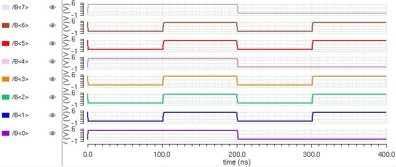
32 0x04 NOT R2, R6 0x06 XOR R3, R2, R5 0x08 JG R3, 0x0C ; * 0x0A OUT R3 0x0C STOP *This jump starts executing at 3.4us, and jumps to the stop instruction, which loads opcode at 2.9us, causing the control unit to generate the GateClock signal. 32
Reference Sheet for C112 Hardware
 Reference Sheet for C112 Hardware 1 Boolean Algebra, Gates and Circuits Autumn 2016 Basic Operators Precedence : (strongest),, + (weakest). AND A B R 0 0 0 0 1 0 1 0 0 1 1 1 OR + A B R 0 0 0 0 1 1 1 0
ECE410 Design Project Spring 2013 Design and Characterization of a CMOS 8-bit pipelined Microprocessor Data Path
 ECE410 Design Project Spring 2013 Design and Characterization of a CMOS 8-bit pipelined Microprocessor Data Path Project Summary This project involves the schematic and layout design of an 8-bit microprocessor
COMPUTER ARCHITECTURE AND ORGANIZATION Register Transfer and Micro-operations 1. Introduction A digital system is an interconnection of digital
 Register Transfer and Micro-operations 1. Introduction A digital system is an interconnection of digital hardware modules that accomplish a specific information-processing task. Digital systems vary in
One and a half hours. Section A is COMPULSORY UNIVERSITY OF MANCHESTER SCHOOL OF COMPUTER SCIENCE
 One and a half hours Section A is COMPULSORY UNIVERSITY OF MANCHESTER SCHOOL OF COMPUTER SCIENCE Fundamentals of Computer Engineering Date: Thursday 21st January 2016 Time: 14:00-15:30 Answer BOTH Questions
 Chapter 1 Microprocessor architecture ECE 3120 Dr. Mohamed Mahmoud http://iweb.tntech.edu/mmahmoud/ mmahmoud@tntech.edu Outline 1.1 Computer hardware organization 1.1.1 Number System 1.1.2 Computer hardware
UNIT-III REGISTER TRANSFER LANGUAGE AND DESIGN OF CONTROL UNIT
 UNIT-III 1 KNREDDY UNIT-III REGISTER TRANSFER LANGUAGE AND DESIGN OF CONTROL UNIT Register Transfer: Register Transfer Language Register Transfer Bus and Memory Transfers Arithmetic Micro operations Logic
Chapter 4. The Processor
 Chapter 4 The Processor Introduction CPU performance factors Instruction count Determined by ISA and compiler CPI and Cycle time Determined by CPU hardware We will examine two MIPS implementations A simplified
REGISTER TRANSFER LANGUAGE
 REGISTER TRANSFER LANGUAGE The operations executed on the data stored in the registers are called micro operations. Classifications of micro operations Register transfer micro operations Arithmetic micro
Microcomputer Architecture and Programming
 IUST-EE (Chapter 1) Microcomputer Architecture and Programming 1 Outline Basic Blocks of Microcomputer Typical Microcomputer Architecture The Single-Chip Microprocessor Microprocessor vs. Microcontroller
Microcomputers. Outline. Number Systems and Digital Logic Review
 Microcomputers Number Systems and Digital Logic Review Lecture 1-1 Outline Number systems and formats Common number systems Base Conversion Integer representation Signed integer representation Binary coded
BUILDING BLOCKS OF A BASIC MICROPROCESSOR. Part 1 PowerPoint Format of Lecture 3 of Book
 BUILDING BLOCKS OF A BASIC MICROPROCESSOR Part PowerPoint Format of Lecture 3 of Book Decoder Tri-state device Full adder, full subtractor Arithmetic Logic Unit (ALU) Memories Example showing how to write
Chapter 5. Digital Design and Computer Architecture, 2 nd Edition. David Money Harris and Sarah L. Harris. Chapter 5 <1>
 Chapter 5 Digital Design and Computer Architecture, 2 nd Edition David Money Harris and Sarah L. Harris Chapter 5 Chapter 5 :: Topics Introduction Arithmetic Circuits umber Systems Sequential Building
ECE 2300 Digital Logic & Computer Organization
 ECE 2300 Digital Logic & Computer Organization Spring 201 Memories Lecture 14: 1 Announcements HW6 will be posted tonight Lab 4b next week: Debug your design before the in-lab exercise Lecture 14: 2 Review:
1. INTRODUCTION TO MICROPROCESSOR AND MICROCOMPUTER ARCHITECTURE:
 1. INTRODUCTION TO MICROPROCESSOR AND MICROCOMPUTER ARCHITECTURE: A microprocessor is a programmable electronics chip that has computing and decision making capabilities similar to central processing unit
Microcontroller Systems
 µcontroller systems 1 / 43 Microcontroller Systems Engineering Science 2nd year A2 Lectures Prof David Murray david.murray@eng.ox.ac.uk www.robots.ox.ac.uk/ dwm/courses/2co Michaelmas 2014 µcontroller
FPGA Programming Technology
 FPGA Programming Technology Static RAM: This Xilinx SRAM configuration cell is constructed from two cross-coupled inverters and uses a standard CMOS process. The configuration cell drives the gates of
Dec Hex Bin ORG ; ZERO. Introduction To Computing
 Dec Hex Bin 0 0 00000000 ORG ; ZERO Introduction To Computing OBJECTIVES this chapter enables the student to: Convert any number from base 2, base 10, or base 16 to any of the other two bases. Add and
Lecture Topics. Announcements. Today: Integer Arithmetic (P&H ) Next: continued. Consulting hours. Introduction to Sim. Milestone #1 (due 1/26)
 Next: continued. Consulting hours. Introduction to Sim. Milestone #1 (due 1/26)") Lecture Topics Today: Integer Arithmetic (P&H 3.1-3.4) Next: continued 1 Announcements Consulting hours Introduction to Sim Milestone #1 (due 1/26) 2 1 Overview: Integer Operations Internal representation
Lecture Topics Today: Integer Arithmetic (P&H 3.1-3.4) Next: continued 1 Announcements Consulting hours Introduction to Sim Milestone #1 (due 1/26) 2 1 Overview: Integer Operations Internal representation
CHAPTER 12 ARRAY SUBSYSTEMS [ ] MANJARI S. KULKARNI
![CHAPTER 12 ARRAY SUBSYSTEMS [ ] MANJARI S. KULKARNI](/thumbs/76/73997056.jpg "CHAPTER 12 ARRAY SUBSYSTEMS [ ] MANJARI S. KULKARNI") CHAPTER 2 ARRAY SUBSYSTEMS [2.4-2.9] MANJARI S. KULKARNI OVERVIEW Array classification Non volatile memory Design and Layout Read-Only Memory (ROM) Pseudo nmos and NAND ROMs Programmable ROMS PROMS, EPROMs,
CHAPTER 2 ARRAY SUBSYSTEMS [2.4-2.9] MANJARI S. KULKARNI OVERVIEW Array classification Non volatile memory Design and Layout Read-Only Memory (ROM) Pseudo nmos and NAND ROMs Programmable ROMS PROMS, EPROMs,
Digital Logic Design Exercises. Assignment 1
 Assignment 1 For Exercises 1-5, match the following numbers with their definition A Number Natural number C Integer number D Negative number E Rational number 1 A unit of an abstract mathematical system
The Processor: Datapath and Control. Jin-Soo Kim Computer Systems Laboratory Sungkyunkwan University
 The Processor: Datapath and Control Jin-Soo Kim (jinsookim@skku.edu) Computer Systems Laboratory Sungkyunkwan University http://csl.skku.edu Introduction CPU performance factors Instruction count Determined
Computer Systems. Binary Representation. Binary Representation. Logical Computation: Boolean Algebra
 Binary Representation Computer Systems Information is represented as a sequence of binary digits: Bits What the actual bits represent depends on the context: Seminar 3 Numerical value (integer, floating
CS 24: INTRODUCTION TO. Spring 2015 Lecture 2 COMPUTING SYSTEMS
 CS 24: INTRODUCTION TO Spring 2015 Lecture 2 COMPUTING SYSTEMS LAST TIME! Began exploring the concepts behind a simple programmable computer! Construct the computer using Boolean values (a.k.a. bits )
Module 5 - CPU Design
 Module 5 - CPU Design Lecture 1 - Introduction to CPU The operation or task that must perform by CPU is: Fetch Instruction: The CPU reads an instruction from memory. Interpret Instruction: The instruction
Basic Processing Unit: Some Fundamental Concepts, Execution of a. Complete Instruction, Multiple Bus Organization, Hard-wired Control,
 UNIT - 7 Basic Processing Unit: Some Fundamental Concepts, Execution of a Complete Instruction, Multiple Bus Organization, Hard-wired Control, Microprogrammed Control Page 178 UNIT - 7 BASIC PROCESSING
Segment 1A. Introduction to Microcomputer and Microprocessor
 Segment 1A Introduction to Microcomputer and Microprocessor 1.1 General Architecture of a Microcomputer System: The term microcomputer is generally synonymous with personal computer, or a computer that
CS 24: INTRODUCTION TO. Spring 2018 Lecture 3 COMPUTING SYSTEMS
 CS 24: INTRODUCTION TO Spring 2018 Lecture 3 COMPUTING SYSTEMS LAST TIME Basic components of processors: Buses, multiplexers, demultiplexers Arithmetic/Logic Unit (ALU) Addressable memory Assembled components
MARIE: An Introduction to a Simple Computer
 MARIE: An Introduction to a Simple Computer 4.2 CPU Basics The computer s CPU fetches, decodes, and executes program instructions. The two principal parts of the CPU are the datapath and the control unit.
Chapter 4. The Processor
 Chapter 4 The Processor Introduction CPU performance factors Instruction count Determined by ISA and compiler CPI and Cycle time Determined by CPU hardware 4.1 Introduction We will examine two MIPS implementations
6.004 Computation Structures Spring 2009
 MIT OpenCourseWare http://ocw.mit.edu 6.004 Computation Structures Spring 2009 For information about citing these materials or our Terms of Use, visit: http://ocw.mit.edu/terms. M A S S A C H U S E T T
Contents. Chapter 9 Datapaths Page 1 of 28
 Chapter 9 Datapaths Page of 2 Contents Contents... 9 Datapaths... 2 9. General Datapath... 3 9.2 Using a General Datapath... 5 9.3 Timing Issues... 7 9.4 A More Complex General Datapath... 9 9.5 VHDL for
1. Internal Architecture of 8085 Microprocessor
 1. Internal Architecture of 8085 Microprocessor Control Unit Generates signals within up to carry out the instruction, which has been decoded. In reality causes certain connections between blocks of the
DESIGN, MANUFACTURE AND TESTING OF A 4-BIT MICROPROCESSOR
 DESIGN, MANUFACTURE AND TESTING OF A 4-BIT MICROPROCESSOR Theodore D ~ntonoli 5th Year Microelectronic Engineering Student Rochester Institute of Technology ABSTRACT A four bit microprocessor was designed
CREATED BY M BILAL & Arslan Ahmad Shaad Visit:
 CREATED BY M BILAL & Arslan Ahmad Shaad Visit: www.techo786.wordpress.com Q1: Define microprocessor? Short Questions Chapter No 01 Fundamental Concepts Microprocessor is a program-controlled and semiconductor
Prototype of SRAM by Sergey Kononov, et al.
 Prototype of SRAM by Sergey Kononov, et al. 1. Project Overview The goal of the project is to create a SRAM memory layout that provides maximum utilization of the space on the 1.5 by 1.5 mm chip. Significant
EE 3170 Microcontroller Applications
 EE 3170 Microcontroller Applications Lecture 4 : Processors, Computers, and Controllers - 1.2 (reading assignment), 1.3-1.5 Based on slides for ECE3170 by Profs. Kieckhafer, Davis, Tan, and Cischke Outline
Topic #6. Processor Design
 Topic #6 Processor Design Major Goals! To present the single-cycle implementation and to develop the student's understanding of combinational and clocked sequential circuits and the relationship between
COSC 243. Computer Architecture 1. COSC 243 (Computer Architecture) Lecture 6 - Computer Architecture 1 1
 Lecture 6 - Computer Architecture 1 1") COSC 243 Computer Architecture 1 COSC 243 (Computer Architecture) Lecture 6 - Computer Architecture 1 1 Overview Last Lecture Flip flops This Lecture Computers Next Lecture Instruction sets and addressing
COSC 243 Computer Architecture 1 COSC 243 (Computer Architecture) Lecture 6 - Computer Architecture 1 1 Overview Last Lecture Flip flops This Lecture Computers Next Lecture Instruction sets and addressing
Register Transfer and Micro-operations
 Register Transfer Language Register Transfer Bus Memory Transfer Micro-operations Some Application of Logic Micro Operations Register Transfer and Micro-operations Learning Objectives After reading this
CHAPTER 5 : Introduction to Intel 8085 Microprocessor Hardware BENG 2223 MICROPROCESSOR TECHNOLOGY
 CHAPTER 5 : Introduction to Intel 8085 Hardware BENG 2223 MICROPROCESSOR TECHNOLOGY The 8085A(commonly known as the 8085) : Was first introduced in March 1976 is an 8-bit microprocessor with 16-bit address
Chapter 1: Basics of Microprocessor [08 M]
![Chapter 1: Basics of Microprocessor [08 M]](/thumbs/77/75860546.jpg "Chapter 1: Basics of Microprocessor [08 M]") Microprocessor: Chapter 1: Basics of Microprocessor [08 M] It is a semiconductor device consisting of electronic logic circuits manufactured by using either a Large scale (LSI) or Very Large Scale (VLSI)
Microprocessor: Chapter 1: Basics of Microprocessor [08 M] It is a semiconductor device consisting of electronic logic circuits manufactured by using either a Large scale (LSI) or Very Large Scale (VLSI)
MEMORIES. Memories. EEC 116, B. Baas 3
 MEMORIES Memories VLSI memories can be classified as belonging to one of two major categories: Individual registers, single bit, or foreground memories Clocked: Transparent latches and Flip-flops Unclocked:
Tailoring the 32-Bit ALU to MIPS
 Tailoring the 32-Bit ALU to MIPS MIPS ALU extensions Overflow detection: Carry into MSB XOR Carry out of MSB Branch instructions Shift instructions Slt instruction Immediate instructions ALU performance
Chapter 4. MARIE: An Introduction to a Simple Computer
 Chapter 4 MARIE: An Introduction to a Simple Computer Chapter 4 Objectives Learn the components common to every modern computer system. Be able to explain how each component contributes to program execution.
Chapter 4. The Processor. Instruction count Determined by ISA and compiler. We will examine two MIPS implementations
 Chapter 4 The Processor Part I Introduction CPU performance factors Instruction count Determined by ISA and compiler CPI and Cycle time Determined by CPU hardware We will examine two MIPS implementations
Computer Architecture Programming the Basic Computer
 4. The Execution of the EXCHANGE Instruction The EXCHANGE routine reads the operand from the effective address and places it in DR. The contents of DR and AC are interchanged in the third microinstruction.
Chapter 4. MARIE: An Introduction to a Simple Computer 4.8 MARIE 4.8 MARIE A Discussion on Decoding
 4.8 MARIE This is the MARIE architecture shown graphically. Chapter 4 MARIE: An Introduction to a Simple Computer 2 4.8 MARIE MARIE s Full Instruction Set A computer s control unit keeps things synchronized,
MARIE: An Introduction to a Simple Computer
 MARIE: An Introduction to a Simple Computer Outline Learn the components common to every modern computer system. Be able to explain how each component contributes to program execution. Understand a simple
CS 31: Intro to Systems Digital Logic. Kevin Webb Swarthmore College February 3, 2015
 CS 31: Intro to Systems Digital Logic Kevin Webb Swarthmore College February 3, 2015 Reading Quiz Today Hardware basics Machine memory models Digital signals Logic gates Circuits: Borrow some paper if
Blog -
 . Instruction Codes Every different processor type has its own design (different registers, buses, microoperations, machine instructions, etc) Modern processor is a very complex device It contains Many
EE577A FINAL PROJECT REPORT Design of a General Purpose CPU
 EE577A FINAL PROJECT REPORT Design of a General Purpose CPU Submitted By Youngseok Lee - 4930239194 Narayana Reddy Lekkala - 9623274062 Chirag Ahuja - 5920609598 Phase 2 Part 1 A. Introduction The core
16.1. Unit 16. Computer Organization Design of a Simple Processor
 6. Unit 6 Computer Organization Design of a Simple Processor HW SW 6.2 You Can Do That Cloud & Distributed Computing (CyberPhysical, Databases, Data Mining,etc.) Applications (AI, Robotics, Graphics, Mobile)
CS 31: Intro to Systems Digital Logic. Kevin Webb Swarthmore College February 2, 2016
 CS 31: Intro to Systems Digital Logic Kevin Webb Swarthmore College February 2, 2016 Reading Quiz Today Hardware basics Machine memory models Digital signals Logic gates Circuits: Borrow some paper if
Introduction to Computer Science. Homework 1
 Introduction to Computer Science Homework. In each circuit below, the rectangles represent the same type of gate. Based on the input and output information given, identify whether the gate involved is
Let s put together a Manual Processor
 Lecture 14 Let s put together a Manual Processor Hardware Lecture 14 Slide 1 The processor Inside every computer there is at least one processor which can take an instruction, some operands and produce
Memory and Programmable Logic
 Memory and Programmable Logic Memory units allow us to store and/or retrieve information Essentially look-up tables Good for storing data, not for function implementation Programmable logic device (PLD),
Digital Logic & Computer Design CS Professor Dan Moldovan Spring 2010
 Digital Logic & Computer Design CS 434 Professor Dan Moldovan Spring 2 Copyright 27 Elsevier 5- Chapter 5 :: Digital Building Blocks Digital Design and Computer Architecture David Money Harris and Sarah
TEACHING COMPUTER ARCHITECTURE THROUGH DESIGN PRACTICE. Guoping Wang 1. INTRODUCTION
 TEACHING COMPUTER ARCHITECTURE THROUGH DESIGN PRACTICE Guoping Wang Indiana University Purdue University Fort Wayne, Indiana; Email:wang@engr.ipfw.edu 1. INTRODUCTION Computer Architecture is a common
A 32-bit Processor: Sequencing and Output Logic
 Lecture 18 A 32-bit Processor: Sequencing and Output Logic Hardware Lecture 18 Slide 1 Last lecture we defined the data paths: Hardware Lecture 18 Slide 2 and we specified an instruction set: Instruction
CAD4 The ALU Fall 2009 Assignment. Description
 CAD4 The ALU Fall 2009 Assignment To design a 16-bit ALU which will be used in the datapath of the microprocessor. This ALU must support two s complement arithmetic and the instructions in the baseline
DC57 COMPUTER ORGANIZATION JUNE 2013
 Q2 (a) How do various factors like Hardware design, Instruction set, Compiler related to the performance of a computer? The most important measure of a computer is how quickly it can execute programs.
Chapter Two - SRAM 1. Introduction to Memories. Static Random Access Memory (SRAM)
") 1 3 Introduction to Memories The most basic classification of a memory device is whether it is Volatile or Non-Volatile (NVM s). These terms refer to whether or not a memory device loses its contents when
1 3 Introduction to Memories The most basic classification of a memory device is whether it is Volatile or Non-Volatile (NVM s). These terms refer to whether or not a memory device loses its contents when
CPE300: Digital System Architecture and Design
 CPE300: Digital System Architecture and Design Fall 2011 MW 17:30-18:45 CBC C316 Number Representation 09212011 http://www.egr.unlv.edu/~b1morris/cpe300/ 2 Outline Recap Logic Circuits for Register Transfer
ASSEMBLY LANGUAGE MACHINE ORGANIZATION
 ASSEMBLY LANGUAGE MACHINE ORGANIZATION CHAPTER 3 1 Sub-topics The topic will cover: Microprocessor architecture CPU processing methods Pipelining Superscalar RISC Multiprocessing Instruction Cycle Instruction
EKT 422/4 COMPUTER ARCHITECTURE. MINI PROJECT : Design of an Arithmetic Logic Unit
 EKT 422/4 COMPUTER ARCHITECTURE MINI PROJECT : Design of an Arithmetic Logic Unit Objective Students will design and build a customized Arithmetic Logic Unit (ALU). It will perform 16 different operations
Introduction to Computers - Chapter 4
 Introduction to Computers - Chapter 4 Since the invention of the transistor and the first digital computer of the 1940s, computers have been increasing in complexity and performance; however, their overall
Design of Digital Circuits 2017 Srdjan Capkun Onur Mutlu (Guest starring: Frank K. Gürkaynak and Aanjhan Ranganathan)
") Microarchitecture Design of Digital Circuits 27 Srdjan Capkun Onur Mutlu (Guest starring: Frank K. Gürkaynak and Aanjhan Ranganathan) http://www.syssec.ethz.ch/education/digitaltechnik_7 Adapted from Digital
Microarchitecture Design of Digital Circuits 27 Srdjan Capkun Onur Mutlu (Guest starring: Frank K. Gürkaynak and Aanjhan Ranganathan) http://www.syssec.ethz.ch/education/digitaltechnik_7 Adapted from Digital
Issue Logic for a 600-MHz Out-of-Order Execution Microprocessor
 IEEE JOURNAL OF SOLID-STATE CIRCUITS, VOL. 33, NO. 5, MAY 1998 707 Issue Logic for a 600-MHz Out-of-Order Execution Microprocessor James A. Farrell and Timothy C. Fischer Abstract The logic and circuits
The MIPS Processor Datapath
 The MIPS Processor Datapath Module Outline MIPS datapath implementation Register File, Instruction memory, Data memory Instruction interpretation and execution. Combinational control Assignment: Datapath
UNIT - V MEMORY P.VIDYA SAGAR ( ASSOCIATE PROFESSOR) Department of Electronics and Communication Engineering, VBIT
 Department of Electronics and Communication Engineering, VBIT") UNIT - V MEMORY P.VIDYA SAGAR ( ASSOCIATE PROFESSOR) contents Memory: Introduction, Random-Access memory, Memory decoding, ROM, Programmable Logic Array, Programmable Array Logic, Sequential programmable
UNIT - V MEMORY P.VIDYA SAGAR ( ASSOCIATE PROFESSOR) contents Memory: Introduction, Random-Access memory, Memory decoding, ROM, Programmable Logic Array, Programmable Array Logic, Sequential programmable
COMPUTER ORGANIZATION AND ARCHITECTURE
 Page 1 1. Which register store the address of next instruction to be executed? A) PC B) AC C) SP D) NONE 2. How many bits are required to address the 128 words of memory? A) 7 B) 8 C) 9 D) NONE 3. is the
Memory. Outline. ECEN454 Digital Integrated Circuit Design. Memory Arrays. SRAM Architecture DRAM. Serial Access Memories ROM
 ECEN454 Digital Integrated Circuit Design Memory ECEN 454 Memory Arrays SRAM Architecture SRAM Cell Decoders Column Circuitry Multiple Ports DRAM Outline Serial Access Memories ROM ECEN 454 12.2 1 Memory
CHAPTER 5 Basic Organization and Design Outline Instruction Codes Computer Registers Computer Instructions Timing and Control Instruction Cycle
 CS 224: Computer Organization S.KHABET CHAPTER 5 Basic Organization and Design Outline Instruction Codes Computer Registers Computer Instructions Timing and Control Instruction Cycle Memory Reference Instructions
ECE369. Chapter 5 ECE369
 Chapter 5 1 State Elements Unclocked vs. Clocked Clocks used in synchronous logic Clocks are needed in sequential logic to decide when an element that contains state should be updated. State element 1
Chapter 1. Microprocessor architecture ECE Dr. Mohamed Mahmoud.
 Chapter 1 Microprocessor architecture ECE 3130 Dr. Mohamed Mahmoud The slides are copyright protected. It is not permissible to use them without a permission from Dr Mahmoud http://www.cae.tntech.edu/~mmahmoud/
Chapter 4. The Processor Designing the datapath
 Chapter 4 The Processor Designing the datapath Introduction CPU performance determined by Instruction Count Clock Cycles per Instruction (CPI) and Cycle time Determined by Instruction Set Architecure (ISA)
Microcontroller Systems. ELET 3232 Topic 11: General Memory Interfacing
 Microcontroller Systems ELET 3232 Topic 11: General Memory Interfacing 1 Objectives To become familiar with the concepts of memory expansion and the data and address bus To design embedded systems circuits
Von Neumann Architecture
 Von Neumann Architecture Assist lecturer Donya A. Khalid Lecture 2 2/29/27 Computer Organization Introduction In 945, just after the World War, Jon Von Neumann proposed to build a more flexible computer.
Chapter 6. CMOS Functional Cells
 Chapter 6 CMOS Functional Cells In the previous chapter we discussed methods of designing layout of logic gates and building blocks like transmission gates, multiplexers and tri-state inverters. In this
1 MALP ( ) Unit-1. (1) Draw and explain the internal architecture of 8085.
 Unit-1. (1) Draw and explain the internal architecture of 8085.") (1) Draw and explain the internal architecture of 8085. The architecture of 8085 Microprocessor is shown in figure given below. The internal architecture of 8085 includes following section ALU-Arithmetic
(1) Draw and explain the internal architecture of 8085. The architecture of 8085 Microprocessor is shown in figure given below. The internal architecture of 8085 includes following section ALU-Arithmetic
Lecture 11 SRAM Zhuo Feng. Z. Feng MTU EE4800 CMOS Digital IC Design & Analysis 2010
 EE4800 CMOS Digital IC Design & Analysis Lecture 11 SRAM Zhuo Feng 11.1 Memory Arrays SRAM Architecture SRAM Cell Decoders Column Circuitryit Multiple Ports Outline Serial Access Memories 11.2 Memory Arrays
The functional block diagram of 8085A is shown in fig.4.1.
 Lecture-13 Internal Architecture of Intel 05A The functional block diagram of 05A is shown in fig.4.1. INTA INTR RST7.5 RST5.5 RST6.5 TRAP SOD SID INTERRUPT SERIAL I/O (Internal Bus) FR(S) IR() B() C()
Systems Programming. Lecture 2 Review of Computer Architecture I
 Systems Programming www.atomicrhubarb.com/systems Lecture 2 Review of Computer Architecture I In The Book Patt & Patel Chapter 1,2,3 (review) Outline Binary Bit Numbering Logical operations 2's complement
VLSI for Multi-Technology Systems (Spring 2003)
") VLSI for Multi-Technology Systems (Spring 2003) Digital Project Due in Lecture Tuesday May 6th Fei Lu Ping Chen Electrical Engineering University of Cincinnati Abstract In this project, we realized the
VLSI for Multi-Technology Systems (Spring 2003) Digital Project Due in Lecture Tuesday May 6th Fei Lu Ping Chen Electrical Engineering University of Cincinnati Abstract In this project, we realized the
Computer Architecture
 Computer Architecture Lecture 1: Digital logic circuits The digital computer is a digital system that performs various computational tasks. Digital computers use the binary number system, which has two
For Example: P: LOAD 5 R0. The command given here is used to load a data 5 to the register R0.
 Register Transfer Language Computers are the electronic devices which have several sets of digital hardware which are inter connected to exchange data. Digital hardware comprises of VLSI Chips which are
ECE260: Fundamentals of Computer Engineering
 Datapath for a Simplified Processor James Moscola Dept. of Engineering & Computer Science York College of Pennsylvania Based on Computer Organization and Design, 5th Edition by Patterson & Hennessy Introduction
Where Does The Cpu Store The Address Of The
 Where Does The Cpu Store The Address Of The Next Instruction To Be Fetched The three most important buses are the address, the data, and the control buses. The CPU always knows where to find the next instruction
Basics of Microprocessor
 Unit 1 Basics of Microprocessor 1. Microprocessor Microprocessor is a multipurpose programmable integrated device that has computing and decision making capability. This semiconductor IC is manufactured
1. Draw general diagram of computer showing different logical components (3)
") Tutorial 1 1. Draw general diagram of computer showing different logical components (3) 2. List at least three input devices (1.5) 3. List any three output devices (1.5) 4. Fill the blank cells of the
Tutorial 1 1. Draw general diagram of computer showing different logical components (3) 2. List at least three input devices (1.5) 3. List any three output devices (1.5) 4. Fill the blank cells of the
McGill University Faculty of Engineering FINAL EXAMINATION Fall 2007 (DEC 2007)
") McGill University Faculty of Engineering FINAL EXAMINATION Fall 2007 (DEC 2007) VERSION 1 Examiner: Professor T.Arbel Signature: INTRODUCTION TO COMPUTER ENGINEERING ECSE-221A 6 December 2007, 1400-1700
McGill University Faculty of Engineering FINAL EXAMINATION Fall 2007 (DEC 2007) VERSION 1 Examiner: Professor T.Arbel Signature: INTRODUCTION TO COMPUTER ENGINEERING ECSE-221A 6 December 2007, 1400-1700
Midterm Project Design of 4 Bit ALU Fall 2001
 Midterm Project Design of 4 Bit ALU Fall 2001 By K.Narayanan George Washington University E.C.E Department K.Narayanan Fall 2001 1 Midterm Project... 1 Design of 4 Bit ALU... 1 Abstract... 3 1.2 Specification:...
CC411: Introduction To Microprocessors
 CC411: Introduction To Microprocessors OBJECTIVES this chapter enables the student to: Use number { base 2, base 10, or base 16 }. Add and subtract binary/hex numbers. Represent any binary number in 2
Processor (I) - datapath & control. Hwansoo Han
 - datapath & control. Hwansoo Han") Processor (I) - datapath & control Hwansoo Han Introduction CPU performance factors Instruction count - Determined by ISA and compiler CPI and Cycle time - Determined by CPU hardware We will examine two
Processor (I) - datapath & control Hwansoo Han Introduction CPU performance factors Instruction count - Determined by ISA and compiler CPI and Cycle time - Determined by CPU hardware We will examine two
Chapter 5. Computer Architecture Organization and Design. Computer System Architecture Database Lab, SANGJI University
 Chapter 5. Computer Architecture Organization and Design Computer System Architecture Database Lab, SANGJI University Computer Architecture Organization and Design Instruction Codes Computer Registers
Single Cycle Datapath
 Single Cycle atapath Lecture notes from MKP, H. H. Lee and S. Yalamanchili Section 4.-4.4 Appendices B.7, B.8, B.,.2 Practice Problems:, 4, 6, 9 ing (2) Introduction We will examine two MIPS implementations
ELCT 501: Digital System Design
 ELCT 501: Digital System Lecture 4: CAD tools (Continued) Dr. Mohamed Abd El Ghany, Basic VHDL Concept Via an Example Problem: write VHDL code for 1-bit adder 4-bit adder 2 1-bit adder Inputs: A (1 bit)
File: 'ReportV37P-CT89533DanSuo.doc' CMPEN 411, Spring 2013, Homework Project 9 chip, 'Tiny Chip' fabricated through MOSIS program
 MOSIS Chip Test Report Dan Suo File: 'ReportV37P-CT89533DanSuo.doc' CMPEN 411, Spring 2013, Homework Project 9 chip, 'Tiny Chip' fabricated through MOSIS program Technology: 0.5um CMOS, ON Semiconductor
CS311 Lecture: The Architecture of a Simple Computer
 CS311 Lecture: The Architecture of a Simple Computer Objectives: July 30, 2003 1. To introduce the MARIE architecture developed in Null ch. 4 2. To introduce writing programs in assembly language Materials:
Computer Organisation CS303
 Computer Organisation CS303 Module Period Assignments 1 Day 1 to Day 6 1. Write a program to evaluate the arithmetic statement: X=(A-B + C * (D * E-F))/G + H*K a. Using a general register computer with