Design Process and Technical Thoughts on a Two Channel PHY Approach
|
|
|
- Wesley Kelley
- 5 years ago
- Views:
Transcription
1 Design Process and Technical Thoughts on a Two Channel PHY Approach Joel Goergen Cisco, Beth Kochuparambil Cisco IEEE 802.3bj January 2012 Interim, Newport Beach, CA, USA
2 Supporters Howard Frazier Broadcom Mark Nowell Cisco Rich Mellitz Intel 2 IEEE 802.3bj January 2012 Interim, Newport Beach, CA, USA
3 Summary Technical View of Nowell_01_0112 Discuss the Design process and technical details supporting a two channel definition from a system vendor and component vendor point of view. This presentation is not advocating one PHY proposal over another but is arguing that the industry will be well served by IEEE developing two PHYs specs. Both PHY proposals have merit and will have broad market potential. 3 IEEE P802.3bj January 2012 Interim, Newport Beach, CA, USA
4 System vendor backplane decision space Review from Nowell_01_0112 Product breadth Generally a system vendor has numerous product families across product portfolio Switching low-end access to high-end core Routing low end access to high-end core Transport low-end access to high-end core Server low-end server to high-end blade server Wide range of initial design dates Platforms designed up to 10 years ago could still be being supported. Plus, backplanes are currently being designed or are in planning today. Once design is locked they are unable to be changed for the lifetime of platform. Backplane is unique Once a platform ships, backplane performance is key factor in EOL decision. Only the backplane and power delivery system have this level of criticality. 4 IEEE P802.3bj January 2012 Interim, Newport Beach, CA, USA
5 Application Debates Deep Dive from Nowell_01_0112 Design considerations Trace length, width, thickness, surface roughness, geometries Boards: board thickness, # of layers, PWB materials / glass / resin, use of counter boring Cost, cost, cost. etc Let s Take a Deep Look at design considerations, or, more importantly, Technology Contribution. Starting with technology trends and the Bill of Materials. 5 IEEE P802.3bj January 2012 Interim, Newport Beach, CA, USA
6 Technology Trends of Circuit Boards Used in Switching, Routing, and Blade Servers Low End or High End Board 1 18by24 Panel Board 2 18by24 Panel VIA Count 56,000 holes 52,600 holes Etched Trace Length 31,000 inches 30,500 inches Net Count 11,100 10,900 Placed Components 12,200 11,900 IEEE 802.3bj January 2012 Interim, Newport Beach, CA, USA

7 The Bill of Materials Breakdown: A Summary from Low End to High End 4.22% 4.10% 12.57% 13.25% 12.69% 15.12% 22.51% 15.55% ASIC Power Mech/Conn/Pkg Memory PCB Other Cables Comm IEEE P802.3bj January 2012 Interim, Newport Beach, CA, USA
8 Now Where to Focus Let s analyze the technology contribution, and the cost of that contribution, specific to circuit boards. Low end designs may trade off technology costs for lower performance. High end designs may need the performance gains that value the technology costs. As you will see in this review circuit board technology increases performance, and also cost. IEEE P802.3bj January 2012 Interim, Newport Beach, CA, USA

9 Technology Contribution: Trace Widths Reasonable Designs Nominal Material IEEE 802.3bj January 2012 Interim, Newport Beach, CA, USA

10 Technology Contribution: Material Cost Material Only Relative Cost Analysis 200% 206% 180% 160% 156% 161% 140% 125% 131% 137% 138% 138% 139% 139% 140% 120% 100% 100% 104% 105% 106% 106% 108% 112% 113% 80% IEEE P802.3bj January 2012 Interim, Newport Beach, CA, USA
11 Focused Material Cost Relative to N Material Only Relative Cost Analysis 200% 209% 180% 160% 137% 137% 140% 120% 100% 104% 100% 80% 60% 40% 20% IEEE P802.3bj January 2012 Interim, Newport Beach, CA, USA

12 Technology Contribution: Drill Usage Drill Bit Life Expectancy Relative Drilled Holes on a Drill Bit 100% 100% 90% 80% 70% 60% 57% 50% 48% 48% 40% 29% 30% 20% IEEE P802.3bj January 2012 Interim, Newport Beach, CA, USA

13 Technology Contribution: Drill Costs Drill Bit Life Expectancy Relative Drilling Costs by Material 20.00% 18.00% 17.30% 16.00% 14.00% 11.50% 13.70% 13.40% 13.70% 12.00% 10.00% 8.00% 6.00% 4.00% 2.00% 0.00% IEEE P802.3bj January 2012 Interim, Newport Beach, CA, USA

14 Technology Contribution: DC Blocking Capacitor Field Consumes a large area Requires considerable grounding to reduce common mode noise, control cross talk, and limit radiated emissions. IEEE P802.3bj January 2012 Interim, Newport Beach, CA, USA

15 Technology Contribution: Glass Construction This glass performs well for 10Gbps. This glass performs well for 10Gbps. 15


16 Technology Contribution: Glass Construction Both Glass types behave well at 10Gbps and appear to work at speeds to 25Gbps Does not perform well at high speeds in part to the Dielectric instability of the glass. 16

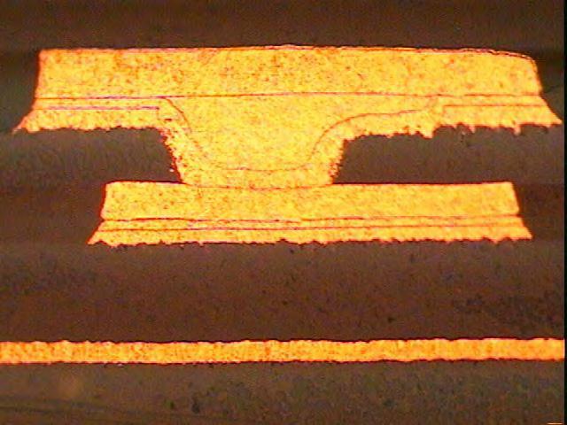
17 Glass Construction: Weave Position Does Make a Difference Figure 1. Cross sectional view of differential signal pair with very equal proximity and alignment to the fiberglass yarn bundle. 17

 VIA")
18 Technology Contribution: VIA in PAD Plated Over (VIPPO) VIA in PAD 18

19 Technology Contribution: VIA in PAD Plated Over Item Signal Integrity Routability Reliability (SnPb) Reliability (Pb-free) Supply Base Process Complexity Cost Comment Eliminate dogbones Very little freed up outer layer area, but requires outer layer features and spaces Proven No issues found yet Large Moderate additional plating, epoxy fill and planarization ~20% adder Adds processing up to 3 extra days Hidden Cons dependant on tech level, layer count, etc Restricted OL feature size Restricted OL spacing 19
 which connect layer 1 to 2 and n to (n-1) Conformal")
20 Technology Contribution: Micro VIA What is it? A standard through hole board with controlled depth vias (laser formed) which connect layer 1 to 2 and n to (n-1) Conformal plated laser via Vias can be conformal plated or Cu fill plated Fill plated laser via 20


21 Technology Contribution: Micro VIA 21
22 Technology Contribution: Micro VIA Item Signal Integrity Routability Reliability (SnPb) Reliability (Pb-free) Supply Base Process Complexity Cost Hidden Cons Comment Small, stubless via Freed up space on layer below via Proven Passed L1 & L2 qualifications Proven - Passed L1 & L2 qualifications Large Minimal laser drilling and microvia plating pretty common technology for most suppliers ~5-15% (Conformal plated) ~15-40% (Cu fill plated) Design tools not 100% optimized 22
")
")
23 Technology Contribution: Skip VIA What is it? Laser vias which connect layer 1 to 3 and n to (n-2) Normally combined with the use of microvias Vias can be conformal plated or epoxy filled and plated over (SKIPPO) Conformal plated skip via 23
24 Technology Contribution: Skip VIA Item Signal Integrity Routability Reliability (SnPb) Reliability (Pb-free) Supply Base Process Complexity Cost Hidden Cons Comment Stubless via connection for high speed signals Freed up space on layer below via Passed Passed Limited Moderate complex laser drilling process ~15-20% (Conformal plated) ~30-40% (SKIPPO) Adds processing days! Up to 3 days. Prone to laminate cracking below via 24
25 Technology Contribution: Back Drilling Spindle With Pressure Foot Spindle With Pressure Foot Backup Material Drill Table Back Drilling is a well defined process with < 4% cost impact on fr4 and < 8% on MEG6. Stop depth tolerance can be as low as +/- 5 mils but often is in the range of +/- 10 mils. Removes a significant portion of the stub. Don t be afraid to deploy this fabrication technology. Seldom used in 2000, this technique is used today in almost all high speed designs. 25


26 1 oz Copper Signal Characteristics Internal Layers 1 oz copper trapezoid shape ~ mils total width reduction at top Copper thickness ~ mils typically 26


27 ½ oz Copper Signal Characteristics Internal Layers ½ oz copper trapezoid shape ~ mils total width reduction at top Copper thickness ~ mils typically 27

28 Technology Contribution: Copper Surface Roughness Much work has been done here. Impact at 10Gbps is not worth the added costs. Impact at 25Gbps shows improvement but still might not be worth the cost. Copper Surface Roughness Relative Cost Analysis 120% 120% 115% 110% 110% 105% 100% 100% 95% 90% 85% 80% 28


29 Technology Contribution: Two Channel Definitions Provide Choices Board Design Challenges 1. Total BOM costs are design specific BOM cost tolerance is program related FCS BOM cost is followed by engineering cost reductions 2. Technology choices can add risks and cost adders 3. Circuit boards are a fundamental component of BOM cost. Improved FR-4 Lower Cost of circuit board implementation and lower signal integrity performance. Limited design constraints. Minimal use of board technology components Usually a board yield in the high 90% range and buildable by a wide range of supplier base. Super Improved FR-4 Higher circuit board costs but much higher signal integrity performance. Can have harsh design constraints to support the performance targets. Utilizes a full set of board technology components in the fabrication. Usually a board yield in the high 60% range and limited in supplier base. IEEE 802.3bj January 2012 Interim, Newport Beach, CA, USA
30 Summary We support and recommend the development of two PHYs targeting two classes of channels, based on two different classes of materials Add an objective! 30 IEEE P802.3bj January 2012 Interim, Newport Beach, CA, USA
31 Thank You! IEEE P802.3bj January 2012 Interim, Newport Beach, CA, USA
100Gb/s Backplane/PCB Ethernet Two Channel Model and Two PHY Proposal
 100Gb/s Backplane/PCB Ethernet Two Channel Model and Two PHY Proposal IEEE P802.3bj 100Gb/s Backplane and Copper Cable Task Force Newport Beach Rich Mellitz, Intel Corporation Kent Lusted, Intel Corporation
I N T E R C O N N E C T A P P L I C A T I O N N O T E. STEP-Z Connector Routing. Report # 26GC001-1 February 20, 2006 v1.0
 I N T E R C O N N E C T A P P L I C A T I O N N O T E STEP-Z Connector Routing Report # 26GC001-1 February 20, 2006 v1.0 STEP-Z CONNECTOR FAMILY Copyright 2006 Tyco Electronics Corporation, Harrisburg,
I N T E R C O N N E C T A P P L I C A T I O N N O T E. Z-PACK TinMan Connector Routing. Report # 27GC001-1 May 9 th, 2007 v1.0
 I N T E R C O N N E C T A P P L I C A T I O N N O T E Z-PACK TinMan Connector Routing Report # 27GC001-1 May 9 th, 2007 v1.0 Z-PACK TinMan Connectors Copyright 2007 Tyco Electronics Corporation, Harrisburg,
I N T E R C O N N E C T A P P L I C A T I O N N O T E. Advanced Mezzanine Card (AMC) Connector Routing. Report # 26GC011-1 September 21 st, 2006 v1.
 Connector Routing. Report # 26GC011-1 September 21 st, 2006 v1.") I N T E R C O N N E C T A P P L I C A T I O N N O T E Advanced Mezzanine Card (AMC) Connector Routing Report # 26GC011-1 September 21 st, 2006 v1.0 Advanced Mezzanine Card (AMC) Connector Copyright 2006
I N T E R C O N N E C T A P P L I C A T I O N N O T E Advanced Mezzanine Card (AMC) Connector Routing Report # 26GC011-1 September 21 st, 2006 v1.0 Advanced Mezzanine Card (AMC) Connector Copyright 2006
I N T E R C O N N E C T A P P L I C A T I O N N O T E. STRADA Whisper 4.5mm Connector Enhanced Backplane and Daughtercard Footprint Routing Guide
 I N T E R C O N N E C T A P P L I C A T I O N N O T E STRADA Whisper 4.5mm Connector Enhanced Backplane and Daughtercard Footprint Routing Guide Report # 32GC001 01/26/2015 Rev 3.0 STRADA Whisper Connector
100GbE Architecture - Getting There... Joel Goergen Chief Scientist
 100GbE Architecture - Getting There... Joel Goergen Chief Scientist April 26, 2005 100GbE Architecture - Getting There Joel Goergen Force10 Networks joel@force10networks.com Subject : 100GbE Architecture
Vertical Conductive Structures
 Vertical Conductive Structures A new Interconnect Technique Agenda The need for an alternative PCB technology Introduction of VeCS Technology comparison Cost comparison State of VeCS technology Application
ATCA Platform Considerations for Backplane Ethernet. Aniruddha Kundu Michael Altmann Intel Corporation May 2004
 ATCA Platform Considerations for Backplane Ethernet Aniruddha Kundu Michael Altmann Intel Corporation May 2004 IEEE 802.3ap Back Plane Ethernet TF Interim meeting May 2004 1 Introduction This presentation
Board Design Guidelines for PCI Express Architecture
 Board Design Guidelines for PCI Express Architecture Cliff Lee Staff Engineer Intel Corporation Member, PCI Express Electrical and Card WGs The facts, techniques and applications presented by the following
Two Backplane Markets, Two Backplane Channels, Two Signaling Schemes, Two PHYs
 Two Backplane Markets, Two Backplane Channels, Two Signaling Schemes, Two PHYs Pravin Patel (IBM), Joel Goergen (Cisco) Howard Frazier (Broadcom) IEEE 802.3bj 100Gb/s Backplane and Copper Cable Task Force
SEAM-RA/SEAF-RA Series Final Inch Designs in PCI Express Applications Generation GT/s
 SEAM-RA/SEAF-RA Series Final Inch Designs in PCI Express Applications Generation 3-8.0 GT/s Copyrights and Trademarks Copyright 2011 Samtec, Inc. Developed in conjunction with Teraspeed Consulting Group
Application Note. PCIE-RA Series Final Inch Designs in PCI Express Applications Generation GT/s
 PCIE-RA Series Final Inch Designs in PCI Express Applications Generation 3-8.0 GT/s Copyrights and Trademarks Copyright 2012, Inc. COPYRIGHTS, TRADEMARKS, and PATENTS Final Inch is a trademark of, Inc.
Application Note. PCIE-EM Series Final Inch Designs in PCI Express Applications Generation GT/s
 PCIE-EM Series Final Inch Designs in PCI Express Applications Generation 3-8.0 GT/s Copyrights and Trademarks Copyright 2015, Inc. COPYRIGHTS, TRADEMARKS, and PATENTS Final Inch is a trademark of, Inc.
Design For Manufacture
 Design For Manufacture Presented by Bill Frank Multek Applications Engineer Discussion Agenda Goals and Objectives DFM Process Flow Board Layout Analysis of Features Board Layout Yield Drivers Electrical
PCIEC PCI Express Jumper High Speed Designs in PCI Express Applications Generation GT/s
 PCIEC PCI Express Jumper High Speed Designs in PCI Express Applications Generation 3-8.0 GT/s Mated with PCIE-RA Series PCB Connectors Copyrights and Trademarks Copyright 2015, Inc. COPYRIGHTS, TRADEMARKS,
Product Application Specification For Connector. Product Application Specification For Connector. Micro cool edge Orthogonal NF1/NGSFF series
 Rev. A1 ECN # CDXXXX 1 of 10 REVISION RECORD REV PAGE DESCRIPTION ECN# DATE Prepared By A ALL FIRST RELEASE CD1143 22.Nov,2017 Yunx.liu A1 ALL Update to Add Micro cool edge CDXXXX 10.Jul,2018 Yunx.liu
Additional Trace Losses due to Glass- Weave Periodic Loading. Jason R. Miller, Gustavo Blando and Istvan Novak Sun Microsystems
 Additional Trace Losses due to Glass- Weave Periodic Loading Jason R. Miller, Gustavo Blando and Istvan Novak Sun Microsystems 1 Introduction PCB laminates are composed of resin and a glass fabric Two
Elma Bustronic CompactPCI Reference Sheet
 Elma Bustronic CompactPCI Reference Sheet Rev. 4 5.10.10 The cpci reference sheet provides relevant reference material for the CompactPCI product line. The information provided may change at anytime. Elma
AT&S Company. Presentation. 3D Component Packaging. in Organic Substrate. Embedded Component. Mark Beesley IPC Apex 2012, San Diego.
 3D Component Packaging AT&S Company in Organic Substrate Presentation Embedded Component Mark Beesley IPC Apex 2012, San Diego www.ats.net Austria Technologie & Systemtechnik Aktiengesellschaft Fabriksgasse13
Lab 9 PCB Design & Layout
 Lab 9 PCB Design & Layout ECT 224L Department of Engineering Technology Lab 9 PCB Traces Size dependent upon electrical requirements, design constraints (routing space and clearance), and trace/space resolution
Power Matters. TM. Why Embedded Die? Piers Tremlett Microsemi 22/9/ Microsemi Corporation. Company Proprietary 1
 Power Matters. TM Why Embedded Die? Piers Tremlett Microsemi 22/9/16 1 Introduction This presentation: Outlines our journey to make miniaturised SiP modules Compares : Embedded Die Technology (EDT) With
ARCHIVE 2010 ABSTRACT
 ARCHIVE 2010 T PCB DESIGN, FABRICATION AND ASSEMBLY Tom Bresnan Sales Manager R&D Circuits by ABSTRACT Guy Ramsey Assembly Division GM R&D Circuits his will cover producing the printed circuits boards
9 rue Alfred Kastler - BP Nantes Cedex 3 - France Phone : +33 (0) website :
 website :") 9 rue Alfred Kastler - BP 10748-44307 Nantes Cedex 3 - France Phone : +33 (0) 240 180 916 - email : info@systemplus.fr - website : www.systemplus.fr August 2011 - Version 1 Written by: Sylvain HALLEREAU
9 rue Alfred Kastler - BP 10748-44307 Nantes Cedex 3 - France Phone : +33 (0) 240 180 916 - email : info@systemplus.fr - website : www.systemplus.fr August 2011 - Version 1 Written by: Sylvain HALLEREAU
The con ectors serve low durability cycle applications
 Power Connectors & Interconnection Systems Introduction to High Current Card Edge Connectors Product Facts Contacts on.100 [2.54] Centerlines Selective gold plating of contacts for high performance at
25 Gb/s Ethernet Study Group CSD: Technical Feasibility. Joel Goergen - Cisco Matt Brown APM Version goergen_25ge_01_0914d
 25 Gb/s Ethernet Study Group CSD: Technical Feasibility Joel Goergen - Cisco Matt Brown APM Version goergen_25ge_01_0914d Supporters Rich Meltz Intel Brad Booth Microsoft Nathan Tracy TE Kent Lusted Intel
ECP Embedded Component Packaging Technology
 ECP Embedded Component Packaging Technology A.Kriechbaum, H.Stahr, M.Biribauer, N.Haslebner, M.Morianz, M.Beesley AT&S Austria Technologie und Systemtechnik AG Abstract The packaging market has undergone
10/100 Application Note General PCB Design and Layout Guidelines AN111
 10/100 Application Note General PCB Design and Layout Guidelines AN111 Introduction This application note provides recommended guidelines in designing a product that complies with both EMI and ESD standards
Report # 20GC004-1 November 15, 2000 v1.0
 I N T E R C O N N E C T A P P L I C A T I O N N O T E Z-PACK HS3 Connector Routing Report # 20GC004-1 November 15, 2000 v1.0 Z-PACK HS3 6 Row 60 Position and 30 Position Connectors Copyright 2000 Tyco
MOLEX COPPER FLEXIBLE CIRCUIT SOLUTIONS
 MOLEX COPPER FLEXIBLE CIRCUIT SOLUTIONS CIRCUITS DESIGNED WITH A RANGE OF CAPABILITIES Maximum Performance for Demanding Applications Flex and Rigid Flex (Typical) Layer Count 1 to 8 Layers Standard Panel
zqsfp+ Behind Bezel Cage Assembly, Heat Sink, and Light Pipe
 zqsfp+ Behind Bezel Cage Assembly, Heat Sink, and Light Pipe Application Specification 114-32023 02 MAR 12 NOTE i All numerical values are in metric units [with U.S. customary units in brackets]. Dimensions
VOLTERA V-ONE PCB PRINTER. Accelerate your hardware development
 VOLTERA V-ONE PCB PRINTER Accelerate your hardware development PRICING AND WHAT S IN THE BOX Conductive Ink Cartridge ( 1) Solder Paste Cartridge ( 1) Dispensers ( 2) z-axis Probe ( 1) Board Clamps ( 2)
ERNIPRESS Trapezoidal-Connectors Series TMC
 ERNIPRESS Trapezoidal-Connectors Series TMC Subminiatur-D Connectors to DIN 41 652/IEC 807-3 with Press-fit zone General Solderless press-in technology for connectors in bus systems permits rationalized
Hardware Design with VHDL PLDs IV ECE 443
 Embedded Processor Cores (Hard and Soft) Electronic design can be realized in hardware (logic gates/registers) or software (instructions executed on a microprocessor). The trade-off is determined by how
Board Mount Connector Footprint Design Process
 Board Mount Connector Footprint Design Process STEP 1: Connector Selection Series Force to Engage (Max) Max SB LD FD Freq. SMP 2.0 lbs 10 lbs 15 lbs 40 GHz SMPM 3.5 lbs N/A 8.0 lbs 65 GHz SMPS 3.0 lbs
Introduction to High Current Card Edge Connectors
 Introduction to High Current Card Edge Connectors Product Facts Contacts on.100 [2.54] Centerlines Selective gold plating of contacts for high performance at low cost Flow solder applications Glass-filled
MAKE A PRINTED-CIRCUIT-BOARD (PCB) FOR YOUR ELECTRONIC DEVICE 11/10/2017 CLIFF CURRY
 FOR YOUR ELECTRONIC DEVICE 11/10/2017 CLIFF CURRY") MAKE A PRINTED-CIRCUIT-BOARD (PCB) FOR YOUR ELECTRONIC DEVICE 11/10/2017 CLIFF CURRY PART ONE: AN INTRODUCTION TO PRINTED CIRCUIT BOARDS. WHAT ARE THEY, AND HOW DOES ONE SPECIFY THEM TO GET WHAT ONE WANTS?
MAKE A PRINTED-CIRCUIT-BOARD (PCB) FOR YOUR ELECTRONIC DEVICE 11/10/2017 CLIFF CURRY PART ONE: AN INTRODUCTION TO PRINTED CIRCUIT BOARDS. WHAT ARE THEY, AND HOW DOES ONE SPECIFY THEM TO GET WHAT ONE WANTS?
inemi Roadmap and Technical Plan on Organic PCB Bill Bader, inemi inemi PCB/Laminate Workshop, Taipei October 22, 2013
 inemi Roadmap and Technical Plan on Organic PCB Bill Bader, inemi inemi PCB/Laminate Workshop, Taipei October 22, 2013 Agenda inemi Roadmap Process and Scope 2013 PCB Roadmap and TIG Outcomes Summary &
FOR PC BOARD TO FLAT CABLE
 AXM FOR PC BOARD TO FLAT CABLE MIL CONNECTORS (AXM) Density mounting Long lever type Short lever type Compliance with RoHS Directive FEATURES 1. High density mounting is possible. Even with mounting right
CENG 4480 Lecture 11: PCB
 CENG 4480 Lecture 11: PCB Bei Yu Reference: Chapter 5 of Ground Planes and Layer Stacking High speed digital design by Johnson and Graham 1 Introduction What is a PCB Why we need one? For large scale production/repeatable
Embedded Passives Become Mainstream Technology, Finally!
 Embedded Passives Become Mainstream Technology, Finally! Joel S. Peiffer 3M Company 3M Center, MS: 201-1E-21 St. Paul, MN 55144 651-575-1464; 651-736-2947 (fax) jspeiffer@mmm.com Abstract Embedded passives,
DAC348x PCB Layout Guidelines for the Multi-Row QFN package
 Texas Instruments Application Report DAC348x PCB Layout Guidelines for the Multi-Row QFN package Russell Hoppenstein Revision 1.0 Abstract This document provides additional information related to the multi-row
BGA Fanout Patterns. Charles Pfeil. Engineering Director Systems Design Division
 BGA Fanout Patterns Charles Pfeil Engineering Director Systems Design Division IPC Irvine Charles Pfeil Background 1966-1987 PCB Designer 1978-1987 Founder of Computer Circuits Inc., Fairfax VA, PCB Design
Published on Online Documentation for Altium Products (https://www.altium.com/documentation)
") Published on Online Documentation for Altium Products (https://www.altium.com/documentation) Home > Defining the Layer Stack Using Altium Documentation Modified by Phil Loughhead on Apr 11, 2017 Related
Published on Online Documentation for Altium Products (https://www.altium.com/documentation) Home > Defining the Layer Stack Using Altium Documentation Modified by Phil Loughhead on Apr 11, 2017 Related
Multi-Drop LVDS with Virtex-E FPGAs
 Multi-Drop LVDS with Virtex-E FPGAs XAPP231 (Version 1.0) September 23, 1999 Application Note: Jon Brunetti & Brian Von Herzen Summary Introduction Multi-Drop LVDS Circuits This application note describes
AN USB332x Transceiver Layout Guidelines
 AN 17.19 USB332x Transceiver Layout Guidelines 1 Introduction SMSC s USB332x comes in a 25 ball Wafer-Level Chip-Scale Package (WLCSP) lead-free RoHS compliant package; (1.95 mm X 1.95 mm, 0.4mm pitch
EDA365. DesignCon Impact of Backplane Connector Pin Field on Trace Impedance and Vertical Field Crosstalk
 DesignCon 2007 Impact of Backplane Connector Pin Field on Trace Impedance and Vertical Field Crosstalk Ravi Kollipara, Rambus, Inc. ravik@rambus.com, (650) 947-5298 Ben Chia, Rambus, Inc. Dan Oh, Rambus,
Application Note AN-1028 Design, Integration and Rework Guidelines for BGA and LGA Packages
 Application Note AN-1028 Design, Integration and Rework Guidelines for BGA and LGA Packages Table of Contents Page Design considerations...2 Substrate...2 PCB layout...2 Solder mask openings...3 Terminations...4
Spring Probes and Probe Cards for Wafer-Level Test. Jim Brandes Multitest. A Comparison of Probe Solutions for an RF WLCSP Product
 AND, AT THE WAFER LEVEL For many in the industry, performing final test at the wafer level is still a novel idea. While providing some much needed solutions, it also comes with its own set of challenges.
EasyCable CompactPCI Backplane
 Description The Elma Bustronic CompactPCI backplane series is designed to be fully compliant with PICMG standards. The EasyCable line features power nuts along the side of the backplane for easy and convenient
z-quad SMALL FORM-FACTOR PLUGGABLE PLUS (zqsfp+ OR QSFP28/56) INTERCONNECT SYSTEM
 INTERCONNECT SYSTEM") z-quad SMALL FORM-FACTOR PLUGGABLE PLUS (zqsfp+ OR QSFP28/56) INTERCONNECT SYSTEM Quick Reference Guide te.com/products/qsfp Introducing zqsfp+ Interconnect System TE Connectivity s (TE) zqsfp+ interconnects
z-quad SMALL FORM-FACTOR PLUGGABLE PLUS (zqsfp+ OR QSFP28/56) INTERCONNECT SYSTEM Quick Reference Guide te.com/products/qsfp Introducing zqsfp+ Interconnect System TE Connectivity s (TE) zqsfp+ interconnects
Product Configuration Solder Tail Press-fit Tail MBCE Vertical Receptacle Yes Yes MBCE Right Angle Receptacle Yes / MBCE Straddle Mount Yes /
 Application Specification 114-128016 28 FEB 17 Rev A3 NOTE All numerical values are in metric units [with U.S. customary units in brackets]. Dimensions are in millimeters [and inches]. Unless otherwise
Power Connectors & Interconnection Systems
 Product Facts Available in latch versions for VRMs up to 3 oz. Available with metal clip for VRMs over 3 oz. VRM connectors to support a wide variety of power supply standards Solder tail, press-fit and
NeXLev Product Specification TB2144
 NeXLev Product Specification TB2144 Revision B Specification Revision Status Revision SCR No. Description Initial Date - S0161 New Release DM 4/5/2006 A S1357 Update copper material callout, DM 8/31/09
Rigid/Bus Bars. Standard Copper Rigid / Bus. PC Board Stiffeners and Current Carrying Busses. Table of Contents. Benefits
 Rigid/Bus Bars Circuit Components Inc. PC Board Stiffeners and Current Carrying Busses Table of Contents Standard Copper Rigid Bus Benefits...1 Part Specifications..2 Part Drawings.3 Snap-In Board Stiffener
KVPX APPLICATION GUIDE
 KVPX APPLICATION GUIDE 1. PRODUCT INFORMATION DAUGHTERCARD MODULES P.N. Description End Shield (Y/N) KX1FCD01C1TBH Daughtercard Center Differential Module N KX1FED01C1TBH Daughtercard End Differential
8-Position Vertical Modular Jack With ACTION PIN* Compliant Contacts
 8-Position Vertical Modular Jack With ACTION PIN* Compliant Contacts Application Specification 11 MAY 11 NOTE i All numerical values are in metric units [with U.S. customary units in brackets]. Dimensions
AN_8430_002 April 2011
 A Maxim Integrated Products Brand 78Q8430 10/100 Ethernet MAC and PHY APPLICATION NOTE AN_8430_002 April 2011 Introduction 78Q8430 Layout Guidelines The TSC 78Q8430 is a single chip 10Base-T/100Base-TX
IT3D(M)-300S-BGA (37) Lead-Free THERMAL CYCLING TEST REPORT
-300S-BGA (37) Lead-Free THERMAL CYCLING TEST REPORT") TR066E-018 ITD(M)-00S-BGA (7) Lead-Free THERMAL CYCLING TEST REPORT - Post 6000 Cycles Report - APPROVED TY.ARAI Nov. 18, 009 CHECKED TM.MATSUO Nov. 17, 009 CHARGED TY.TAKADA Nov. 17, 009 HIROSE ELECTRIC
TR066E-018 ITD(M)-00S-BGA (7) Lead-Free THERMAL CYCLING TEST REPORT - Post 6000 Cycles Report - APPROVED TY.ARAI Nov. 18, 009 CHECKED TM.MATSUO Nov. 17, 009 CHARGED TY.TAKADA Nov. 17, 009 HIROSE ELECTRIC
This application note is written for a reader that is familiar with Ethernet hardware design.
 AN 14.8 LAN8700/LAN8700I and LAN8187/LAN8187I Ethernet PHY Layout Guidelines 1 Introduction 1.1 Audience 1.2 Overview The LAN8700/LAN8700I and LAN8187/LAN8187I are highly-integrated devices designed for
APPLICATION SPECIFICATION. 1 of 33 J (r/a header, r/a receptacle, vertical header, vertical receptacle TABLE OF CONTENTS 1. OBJECTIVE...
 1 of 33 J Section TABLE OF CONTENTS page no. 1. OBJECTIVE...2 2. SCOPE...2 3. APPLICABLE DOCUMENTS...3 4. GENERAL CUSTOMER INFORMATION...3 4.1. CONNECTOR CONFIGURATIONS...3 4.2. COMPATIBILITY WITH HARD
Enabling SI Productivity Part 2. Venkatesh Seetharam Aaron Edwards
 Enabling SI Productivity Part 2 Venkatesh Seetharam Aaron Edwards 1 Problem Statement SI engineers use simulation software to squeeze the most performance out of their design. They will tend to focus on
Ultra-thin Capacitors for Enabling Miniaturized IoT Applications
 Ultra-thin Capacitors for Enabling Miniaturized IoT Applications Fraunhofer Demo Day, Oct 8 th, 2015 Konrad Seidel, Fraunhofer IPMS-CNT 10/15/2015 1 CONTENT Why we need thin passive devices? Integration
Guidelines for project
 Guidelines for project objectives Hugh Barrass & Howard Frazier EPON Protocol over Coax (EPoC) PHY Study Group Newport Beach, CA 24-January-2012 1 Outline History and traditions Guidelines for writing
Current Practices Model Anatomy
 Current Practices Model Anatomy Aniruddha Kundu Intel Corporation 11-16-2004 IEEE 802.3ap Back Plane Ethernet TF November, 2004 1 Contributors: Jeff Lynch, Praveen Patel: IBM John D Ambrosia: Tyco Electronics
Getting Started. 1.3 X-MWsystem Vocabulary. X-MWprobe X-MWanchor X-MWjumper. X-MWblock RF. X-MWblock Bias and Control. X-MWprotoplate X-MWwall X-MWlid
 1. X-Microwave System (X-MWsystem) 1.1 Overview RF and Microwave design and product development is an incredibly interesting and challenging field. The Craft is truly an art and it takes years to learn
Impact of Embedded Capacitance on Test Socket and Test Board Performance Michael Giesler, 3M, Alexander Barr, 3M Yoshihisa Kawate,
 Impact of Embedded Capacitance on Test Socket and Test Board Performance Michael Giesler, 3M, msgiesler@mmm.com Alexander Barr, 3M Yoshihisa Kawate, Sumitomo-3M Yuichi Tsubaki, Sumitomo-3M Silicon Valley
Elcon CROWN EDGE Card Edge-style High Current Connectors
 Elcon CROWN EDGE Card Edge-style High Current Connectors CROWN EDGE is a board-to-board power interconnect solution that uses Elcon high performance Crown contact technology configured to mate directly
Session 4a. Burn-in & Test Socket Workshop Burn-in Board Design
 Session 4a Burn-in & Test Socket Workshop 2000 Burn-in Board Design BURN-IN & TEST SOCKET WORKSHOP COPYRIGHT NOTICE The papers in this publication comprise the proceedings of the 2000 BiTS Workshop. They
Custom Connectors Overview
 Company Overview March 12, 2015 Custom Connectors Overview Tuesday, October 03, 2017 CONNECTOR OVERVIEW Engineering Manufacturing Connector Products HiLo FlexFrame Custom Connectors Standard Connectors
Using MLOs to Build Vertical Technology Space Transformers
 Presentation to Southwest Test Workshop 2002 Using MLOs to Build Vertical Technology Space Transformers Bill Fulton and Bill Pardee Wentworth Laboratories Overview 1. Terminology 2. Benefits of MLOs vs
Sequence Estimators with Block Termination in the presence of ISI
 Hardware implementation i of Sequence Estimators with Block Termination in the presence of ISI Presentation to IEEE 802.3bj Arash Farhood Cortina Systems Joel Goergen Cisco Elizabeth Kochuparambil - Cisco
EXAMINING THE IMPACT OF SPLIT PLANES ON SIGNAL AND POWER INTEGRITY
 EXAMINING THE IMPACT OF SPLIT PLANES ON SIGNAL AND POWER INTEGRITY Jason R. Miller, Gustavo J. Blando, Roger Dame, K. Barry A. Williams and Istvan Novak Sun Microsystems, Burlington, MA 1 AGENDA Introduction
Understanding 3M Ultra Hard Metric (UHM) Connectors
 Connectors") 3M Electronic Solutions Division 3MUHMWEBID_100809 Understanding 3M Ultra Hard Metric (UHM) Connectors Enabling performance of next generation 2 mm Hard Metric systems 3M Electronic Solutions Division
3M Electronic Solutions Division 3MUHMWEBID_100809 Understanding 3M Ultra Hard Metric (UHM) Connectors Enabling performance of next generation 2 mm Hard Metric systems 3M Electronic Solutions Division
Made in Italy INSPECTA COMBO X-RAY DRILLER - ROUTER ASSISTED BY X-RAY OPTIMIZATION
 Made in Italy DRILLER - ROUTER ASSISTED BY OPTIMIZATION ALL LINEAR MOTORS The latest and most flexible x-ray unit for drilling / routing. INSPECTA COMBO High speed drill/rout air bearing spindles 20,000
Pixus Technologies Catalog
 The Power of Embedded Ingenuity Pixus Technologies Catalog Kaparel, Ripac, & Vario Brand Products www.pixustechnologies.com sales@pixustechnologies.com US: 916.524.8242 CAN: 519.885.5775 Order Information
25G Ethernet CFI. Final Draft Brad Booth, Microsoft. Photo courtesy of Hugh Barrass
 25G Ethernet CFI Final Draft Brad Booth, Microsoft Photo courtesy of Hugh Barrass Objectives To gauge the interest in starting a study group to investigate a 25 Gigabit Ethernet project Don t need to:
Revolutionary High Performance Interconnect Which Maximizes Signal Density
 Revolutionary High Performance Interconnect Which Maximizes Signal Density Tom Cohen and Gautam Patel Teradyne Connection Systems 44 Simon St. Nashua, New Hampshire 03060 Phone: 603-791-3383, 603-791-3164
PCB Temperature Compatibility with Lead-Free Soldering. Jeffrey Taylor, Marie Cole, Matt Kelly, Wai Ma, John Wilson
 Jeffrey Taylor, Marie Cole, Matt Kelly, Wai Ma, John Wilson 2004 IBM Corporation Acknowledgments Kaspar Tsang Alex Chu Paula Nixa PS Hou Brian Carlson Kevin Splittstoesser David Braun Jason Chou Cuemee
The Dawn of Channelized Ethernet
 The Dawn of Channelized Ethernet Nathan Farrington Hot Interconnects 22, Mountain View, CA, USA, August 26-27, 2014 Outline This talk is mostly about parallelism. EtherChannel: Parallelism Going Up Kalpana
Area Array Probe Card Interposer. Raphael Robertazzi IBM Research 6/4/01. 6/4/01 IBM RESEARCH Page [1]
![Area Array Probe Card Interposer. Raphael Robertazzi IBM Research 6/4/01. 6/4/01 IBM RESEARCH Page [1]](/thumbs/78/78371092.jpg "Area Array Probe Card Interposer. Raphael Robertazzi IBM Research 6/4/01. 6/4/01 IBM RESEARCH Page [1]") Area Array Probe Card Interposer Raphael Robertazzi IBM Research 6/4/01 6/4/01 IBM RESEARCH Page [1] Motivation: Outline Probe Cards for Testing Complex ICs in the Developmental Stage. Hand Wired Space
Area Array Probe Card Interposer Raphael Robertazzi IBM Research 6/4/01 6/4/01 IBM RESEARCH Page [1] Motivation: Outline Probe Cards for Testing Complex ICs in the Developmental Stage. Hand Wired Space
Board Design Guidelines for Intel Programmable Device Packages
 Board Design Guidelines for Intel Programmable Device Packages AN-114 2017.02.24 Subscribe Send Feedback Contents Contents 1 Board Design Guidelines for Intel Programmable Device Packages...3 1.1 Overview
2 Channel Headset EMI Filter with ESD Protection
 2 Channel Headset EMI Filter with ESD Protection Features Two channels of EMI filtering, one for a microphone and one for an earpiece speaker Pi-style EMI filters in a capacitor-resistor-capacitor (C-R-C)
100G backplane PHY: NRZ and PAM4
 100G backplane PHY: NRZ and PAM4 Matt Brown 802.3bj Task Force IEEE 802.3 Interim September 2011 1 Contributors and Supporters Richard Mellitz, Intel Corp. Howard Frazier, Broadcom Will Bliss, Broadcom
Model XDL S Rev A
 Delay Line DESCRIPTION The XDL15-3-030S can be used in amplifier linearization applications from 135 2700Mhz. Small form factor of XDL15-3-030S is ideal for cascading to obtain longer delay. The Xinger
Krzysztof Dabrowiecki, Probe2000 Inc Southwest Test Conference, San Diego, CA June 08, 2004
 Structural stability of shelf probe cards Krzysztof Dabrowiecki, Probe2000 Inc Southwest Test Conference, San Diego, CA June 08, 2004 Presentation Outline Introduction Objectives Multi die applications
High-Density Design with MicroStar BGAs
 High-Density Design with MicroStar BGAs Gerald Capwell Fixed-Point DSP Applications Abstract The consumer electronics industry constantly faces new challenges to design their solutions smaller and less
KVPX APPLICATION GUIDE
 KVPX APPLICATION GUIDE 1. PRODUCT INFORMATION DAUGHTERCARD MODULES P.N. Description End Shield (Y/N) KX1FCD01C1TBH Daughtercard Center Differential Module N KX1FED01C1TBH Daughtercard End Differential
Today: Multi-touch capacitive touch screens How do they work?
 1975: Capacitive touch switches in use 1994: 1st laptop capacitive touchpad 2003: 1st ipod capacitive touchwheel Today: Multi-touch capacitive touch screens How do they work? CNMAT Sensor Workshop 2008
Termination End. Figure 1
 AMP- LATCH* Application Specification Universal Headers 114-40020 with ACTION PIN* Contacts 19 DEC 11 Rev D NOTE i All numerical values are in metric units [with U.S. customary units in brackets]. Dimensions
Second edition. Charles Pfeil
 Second edition Charles Pfeil BGA Breakouts and Routing Effective Design Methods for Very Large BGAs Second Edition Version 5.1 Charles Pfeil 5/12/2010 Very large BGAs, over 1500 pins, present a unique
Orbis MU 21. Digital Delegate Microphone Unit with Loudspeaker Order #
 Digital Delegate Microphone Unit with Loudspeaker Order # 725.706 Supplied without gooseneck microphone FEATURES Coated plastic housing with metal bottom plate Inserts made of optically hardened acrylic
1.27mm Pitch Two-Piece Connector
 1.7mm Pitch Two-Piece Connector HIF6 Series Connector in combination with the HIF6 series connection type HIF3B Series (MIL-C-83503) HIF Series (Board direct mount type) HIF5 Series 1 (Card edge type)
Quad Module Hybrid Development for the ATLAS Pixel Layer Upgrade
 Quad Module Hybrid Development for the ATLAS Pixel Layer Upgrade Lawrence Berkeley National Lab E-mail: kedunne@lbl.gov Maurice Garcia-Sciveres, Timon Heim Lawrence Berkeley National Lab, Berkeley, USA
1.27mm Pitch Two-Piece Connectors
 1.7mm Pitch Two-Piece Connectors HIF6 Series Connector in combination with the HIF6 series connection type HIF3B Series (MIL-C-833) HIF Series (Board direct mount type) Features 1. Product Variation The
LQFP. Thermal Resistance. Body Size (mm) Pkg. 32 ld 7 x 7 5 x ld 7 x 7 5 x ld 14 x 14 8 x ld 20 x x 8.5
 Pkg. 32 ld 7 x 7 5 x ld 7 x 7 5 x ld 14 x 14 8 x ld 20 x x 8.5") LQFP Low Profile Quad Flat Pack Packages (LQFP) Amkor offers a broad line of LQFP IC packages designed to provide the same great benefits as MQFP packaging with a 1.4 mm body thickness. These packages
LQFP Low Profile Quad Flat Pack Packages (LQFP) Amkor offers a broad line of LQFP IC packages designed to provide the same great benefits as MQFP packaging with a 1.4 mm body thickness. These packages
1.27mm Pitch Two-Piece Connector
 All non-rohs products have been discontinued, or will be discontinued soon. Please check the products status on the Hirose website RoHS search at www.hirose-connectors.com, or contact your Hirose sales
Z- DOK* and Z- DOK + Connectors 14 APR 11 Rev C
 Application Specification 114-13068 Z- DOK* and Z- DOK + Connectors 14 APR 11 Rev C NOTE i All numerical values are in metric units [with U.S. customary units in brackets]. Dimensions are in millimeters.
The Hidden Component of High Speed Filter Design: The Footprint Influence
 CARTS USA 2010, March 15 th 18 th, 2010 Presentation The Hidden Component of High Speed Filter Design: The Footprint Influence Michael Howieson, Akhlaq Rahman, Mark Broman Thin Film Technology Corporation
Q2 QMS/QFS 16mm Stack Height Final Inch Designs In PCI Express Applications Generation Gbps. Revision Date: February 13, 2009
 Q2 QMS/QFS 16mm Stack Height Final Inch Designs In PCI Express Applications Generation 2 5.0 Gbps Revision Date: February 13, 2009 Copyrights and Trademarks Copyright 2009 Samtec, Inc. Developed in conjunction
MT2 Introduction Embedded Systems. MT2.1 Mechatronic systems
 MT2 Introduction Embedded Systems MT2.1 Mechatronic systems Mechatronics is the synergistic integration of mechanical engineering, with electronics and intelligent computer control in the design and manufacturing