Ultra-thin Capacitors for Enabling Miniaturized IoT Applications
|
|
|
- Ezra Lambert
- 5 years ago
- Views:
Transcription

1 Ultra-thin Capacitors for Enabling Miniaturized IoT Applications Fraunhofer Demo Day, Oct 8 th, 2015 Konrad Seidel, Fraunhofer IPMS-CNT 10/15/2015 1
2 CONTENT Why we need thin passive devices? Integration options for passives Discrete thin-film capacitor platform technology High-k dielectrics Area gain by 3D integration Electrical results 10/15/2015 2

3 The World of IoT 10/15/2015 3

4 The World of IoT On average, each cow generates about 200 megabytes of information each year 10/15/2015 4


5 Miniaturized Application examples GPS Module Source: ESP8266 WIFI Module Ant-size radio Source: CSIRO / Engadget Implantable pressure sensors Source: 4D Systems Miniaturized chip for hearing aids Source: Stanford Univ. Source: Sensors 2014, 14, Source: Fraunhofer IZM 10/15/2015 5
6 IoT is an evolution Source: SRI Consulting Business Intelligence/National Intelligence Council 10/15/2015 6
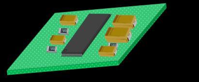
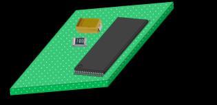


7 Miniaturization of Integrated Systems Example: WIFI modem? (EPCOS AG) (EPCOS AG) (EPCOS AG) Main Enablers More functions on chip Scaling of semiconductors New packaging technologies Integration of Passive components ( L, C, R ) 10/15/2015 7
8 Integrated Capacitors Applications & maximum available Si-based capacitors on chip or in package Capacitance density RF filtering matching & Analog filtering Bypassing, decoupling Charge-pumping & storage 10µF/mm² 1µF/mm² To support wide capacitance range GPUs, CPUS, DC/DC converters Sensors, Medical 100nF/mm² 10nF/mm² 1nF/mm² RF transceivers Audio filters Microcontroller Baseband ICs Si-Interposer ASICs 100pF/mm² power amplifiers Source: Fraunhofer IPMS-CNT / Yole development 10/15/2015 8


, STO (>100) C 0k 10/15/2015 9 A d 3.")

9 Capacitance Tuning How to address wide capacitance range? 2D 3D Dielectric Bottom Electrode 1. Dielectric constant Conventional: SiO 2 (k=3.9) HfSiON (k=7) Ta 2 O 5 (k=26) TiO 2 (k=80), STO (>100) C 0k 10/15/ A d 3. Thickness tuning Operating conditions Reliability! 2. Surface Area 3D integration Structures with high Aspect ratio
10 System integration options for capacitors Integrated Discrete System on Chip (SoC) Chip-on-Board Low Power Chip Capacitor Chip Substrate / Lead Frame System in Package (SiP) Thin substrates <100µm required in order to meet dense packaging requirements Interposer Integration Embedding in PCB [1] Customized solution No ext. discrete components Specialized for one technology Standardized outline (SMD package - EIA standard) Addressing multiple integration options, low costs Consumes more space compared to SoC 10/15/ [1] Source: M. Brizoux et al, Proceedings of Smart Systems Integration 2009
 Chip-on-Board Low Power Chip Capacitor Chip Substrate /")

 Addressing multiple")

11 Platform Technology Concept Integrated Discrete System on Chip (SoC) Chip-on-Board Low Power Chip Capacitor Chip Substrate / Lead Frame System in Package (SiP) Interposer Integration Embedding in PCB [1] Customized solution No ext. discrete components Specialized for one technology Standardized outline (SMD package - EIA standard) Addressing multiple integration options, low costs Consumes more space compared to SoC 10/15/ [1] Source: M. Brizoux et al, Proceedings of Smart Systems Integration 2009


12 Front-End processing <100µm Platform Technology Concept Standardized Capacitor Module 1. Raw Silicon Wafer 2. Etch deep holes 3. Electrodes & dielectric 4. Electrode Patterning Standard Silicon Processing Technology Back-End processing Metallization & Contacts Grinding Dicing TF-SMD capacitor Interposer 10/15/


13 <100µm Platform Technology Concept Standardized Capacitor Module 3D solution Laser (stealth) dicing Conventional Blade Laser Source: Photonics.com/ Hamamatsu Planar solution No edge loss Low damage No chipping & µ-cracks TF-SMD capacitor Interposer 10/15/


14 TSV Capacitor component Standard SMD outline /15/
15 TSV Capacitor component Top Contact (Cu) Standard SMD outline Bottom Contact (Cu) /15/
 Bottom Contact")

16 TSV Capacitor component Top Contact (Cu) Bottom Contact (Cu) Single-sided contacts Double-sided contacts 10/15/


17 TSV Capacitor component Top Contact (Cu) Chip labeling for ease of handling Bottom Contact (Cu) 10x10 0 pf = 10pF 47pF 100pF 10/15/
18 Capacitor component Example of achievable capacitances Component / Technology Value Range Voltage Thickness pf 5V 100µm planar planar planar planar 10 pf 5V 100µm planar planar planar planar 47 pf 5V 100µm planar planar planar planar 100 pf 5V 100µm planar planar planar planar 470 pf 5V 100µm planar planar planar planar 1 nf 5V 100µm planar planar planar planar 2.2 nf 5V 100µm 3D planar planar planar 4.7 nf 5V 100µm 3D 3D planar planar 10 nf 5V 100µm 3D 3D 3D planar 22 nf 5V 100µm 3D 3D planar 47 nf 5V 100µm 3D 3D 100 nf 5V 100µm 3D 3D 470 nf 5V 100µm 3D 1 µf 4V 100µm 3D 20 µf 4V 100µm 3D / interposer Customizable: Other values, voltages & dimensions on request 10/15/


19 DEVELOPMENT & PILOT FABRICATION Capacitor Front-End processing ENVIRONMENT Capacitor Back-End processing 300 mm IPMS-CNT cleanroom 800 m² clean room, class 1000 & 650 m² laboratory area 40 Tools for Wafer Processing, Patterning, Metrology & Analytics Qualification of processes & materials on 300 mm industrial standard equipment Wafer level packaging & CSP 3D IC and heterogeneous integration Silicon & glass interposer Thin wafer processing & handling 3D stacking, hermetical sealing 10/15/


20 (a.u.) Time to breakdown Planar Capacitors high-k materials C 0k A d Top Electrode High-k Material stack by ALD Bottom Elektrode ALD atomic layer deposition Increased Capacitance density Lower Breakdown Voltage Steeper Field acceleration Trade-off between capacitance density and reliability thickness scaling Source: J. McPherson, IEDM /15/
21 Planar Capacitors Electrical results 5 4 I leak I leak (na/µf) Bias (V) 10/15/

 1E-07 1E-08 1E-09 1E-10 I leak @ 2.")

 Comparison: Typ.")
22 Planar Capacitors Electrical results I leak (na/µf) I leak dc/c 0 <2.5% Bias (V) dc/c 0 (%) I leak (A/cm²) 1E-07 1E-08 1E-09 1E-10 I 2.5V I 5V dc/c 25 C +/- 3% E Temperature ( C) dc/c 25 C (%) Comparison: Typ. Ceramic MLCC Capacitor (X7R) Temperature: +/- 10% tolerance DC Voltage: up to 50% drop 10/15/


23 Going for 3D Area gain by hole integration C 0k A d Small-size holes with high aspect-ratio Allowing ultra-thin substrates Conformal deposition Of dielectric requires Enabled by ALD 10/15/
 D=120nm D=130nm D=140nm D=150nm D=160nm D=170nm")


24 3D Capacitors Density optimization Type A Type C Type B C (nf/mm 2 ) D=120nm D=130nm D=140nm D=150nm D=160nm D=170nm P=220nm P=240nm CD and Pitch optimization for further capacitance density enhancement Capacitance Leakage Pitch P= 230nm Pattern collapse D = 150nm P=260nm I leak (na/µf) 10/15/
")
25 2mm 3D Capacitors Test on large area demonstrator J (A/µF) 1E-6 AR 13:1 AR 15:1 AR 20:1 1E-7 4mm² Demo AR20:1 1E-8 2mm 1E-9 1E-10 No impact of aspect ratio scaling on electrical performance Large area demonstrator shows good matching to results on test structures Bias (V) 10/15/
![Reliability time to dielectric breakdown 1E-5 Stress test @ accelerated conditions J[A/cm²] 1E-6 Time to Failure (s) Good agreement between planar 10-1 and](/docs-images/81/83633571/images/26-3.jpg "3D capacitor reliability 1.0 1.5 2.0 2.5 3.0 3.")
26 Reliability time to dielectric breakdown 1E-5 Stress accelerated conditions J[A/cm²] 1E-6 Time to Failure (s) Good agreement between planar 10-1 and 3D capacitor reliability E-7 Planar 3D-Capacitor t [s] Electric Field (MV/cm) 10 years 10/15/
27 <100µm SUMMARY TF-SMD capacitor Interposer IoT evolution is driving system miniaturization small components Addressing various integration options SoC high density capacitors in BEOL Discrete: embedding in substrates and interposer Wide capacitance bandwith due to high-k materials and area gain Ultra-thin substrates due to small holes with high aspect ratio 10/15/

28 MANY THANKS FOR YOUR ATTENTION contact: Special thanks to the project teams of: Visit our booth 2092 This work was supported by the Fraunhofer internal MAVO program SmartTicket 10/15/
Development of innovative ALD materials for high density 3D integrated capacitors
 Development of innovative ALD materials for high density 3D integrated capacitors Malte Czernohorsky General Trend: System miniaturization Integration of passive components Capacitors Inductors Resistors
Applications, Processing and Integration Options for High Dielectric Constant Multi-Layer Thin-Film Barium Strontium Titanate (BST) Capacitors
 Capacitors") Applications, Processing and Integration Options for High Dielectric Constant Multi-Layer Thin-Film Barium Strontium Titanate (BST) Capacitors Agenda Introduction What is BST? Unique Characteristics of
Applications, Processing and Integration Options for High Dielectric Constant Multi-Layer Thin-Film Barium Strontium Titanate (BST) Capacitors Agenda Introduction What is BST? Unique Characteristics of
TechSearch International, Inc.
 Silicon Interposers: Ghost of the Past or a New Opportunity? Linda C. Matthew TechSearch International, Inc. www.techsearchinc.com Outline History of Silicon Carriers Thin film on silicon examples Multichip
DEPARTMENT WAFER LEVEL SYSTEM INTEGRATION
 FRAUNHOFER INSTITUTE FOR RELIABILITY AND MICROINTEGRATION IZM DEPARTMENT WAFER LEVEL SYSTEM INTEGRATION ALL SILICON SYSTEM INTEGRATION DRESDEN ASSID ALL SILICON SYSTEM INTEGRATION DRESDEN FRAUNHOFER IZM-ASSID
3D technology evolution to smart interposer and high density 3D ICs
 3D technology evolution to smart interposer and high density 3D ICs Patrick Leduc, Jean Charbonnier, Nicolas Sillon, Séverine Chéramy, Yann Lamy, Gilles Simon CEA-Leti, Minatec Campus Why 3D integration?
Embedded UTCP interposers for miniature smart sensors
 Embedded UTCP interposers for miniature smart sensors T. Sterken 1,2, M. Op de Beeck 2, Tom Torfs 2, F. Vermeiren 1,2, C. Van Hoof 2, J. Vanfleteren 1,2 1 CMST (affiliated with Ugent and IMEC), Technologiepark
Embedded Power Dies for System-in-Package (SiP)
") Embedded Power Dies for System-in-Package (SiP) D. Manessis, L. Boettcher, S. Karaszkiewicz, R.Patzelt, D. Schuetze, A. Podlasky, A. Ostmann Fraunhofer Institute for Reliability and Microintegration (IZM),
Embedded Power Dies for System-in-Package (SiP) D. Manessis, L. Boettcher, S. Karaszkiewicz, R.Patzelt, D. Schuetze, A. Podlasky, A. Ostmann Fraunhofer Institute for Reliability and Microintegration (IZM),
Moore s Law: Alive and Well. Mark Bohr Intel Senior Fellow
 Moore s Law: Alive and Well Mark Bohr Intel Senior Fellow Intel Scaling Trend 10 10000 1 1000 Micron 0.1 100 nm 0.01 22 nm 14 nm 10 nm 10 0.001 1 1970 1980 1990 2000 2010 2020 2030 Intel Scaling Trend
3D SYSTEM INTEGRATION TECHNOLOGY CHOICES AND CHALLENGE ERIC BEYNE, ANTONIO LA MANNA
 3D SYSTEM INTEGRATION TECHNOLOGY CHOICES AND CHALLENGE ERIC BEYNE, ANTONIO LA MANNA OUTLINE 3D Application Drivers and Roadmap 3D Stacked-IC Technology 3D System-on-Chip: Fine grain partitioning Conclusion
SEMI 大半导体产业网 MEMS Packaging Technology Trend
 MEMS Packaging Technology Trend Authors Name: KC Yee Company Name: ASE Group Present Date:9/9/2010 1 Overview Market Trend Packaging Technology Trend Summary 2 2 MEMS Applications Across 4C Automotive
From 3D Toolbox to 3D Integration: Examples of Successful 3D Applicative Demonstrators N.Sillon. CEA. All rights reserved
 From 3D Toolbox to 3D Integration: Examples of Successful 3D Applicative Demonstrators N.Sillon Agenda Introduction 2,5D: Silicon Interposer 3DIC: Wide I/O Memory-On-Logic 3D Packaging: X-Ray sensor Conclusion
3D technology for Advanced Medical Devices Applications
 3D technology for Advanced Medical Devices Applications By, Dr Pascal Couderc,Jerome Noiray, Dr Christian Val, Dr Nadia Boulay IMAPS MEDICAL WORKSHOP DECEMBER 4 & 5,2012 P.COUDERC 3D technology for Advanced
Multi-Die Packaging How Ready Are We?
 Multi-Die Packaging How Ready Are We? Rich Rice ASE Group April 23 rd, 2015 Agenda ASE Brief Integration Drivers Multi-Chip Packaging 2.5D / 3D / SiP / SiM Design / Co-Design Challenges: an OSAT Perspective
3D Integration & Packaging Challenges with through-silicon-vias (TSV)
") NSF Workshop 2/02/2012 3D Integration & Packaging Challenges with through-silicon-vias (TSV) Dr John U. Knickerbocker IBM - T.J. Watson Research, New York, USA Substrate IBM Research Acknowledgements IBM
NSF Workshop 2/02/2012 3D Integration & Packaging Challenges with through-silicon-vias (TSV) Dr John U. Knickerbocker IBM - T.J. Watson Research, New York, USA Substrate IBM Research Acknowledgements IBM
WLSI Extends Si Processing and Supports Moore s Law. Douglas Yu TSMC R&D,
 WLSI Extends Si Processing and Supports Moore s Law Douglas Yu TSMC R&D, chyu@tsmc.com SiP Summit, Semicon Taiwan, Taipei, Taiwan, Sep. 9 th, 2016 Introduction Moore s Law Challenges Heterogeneous Integration
Bringing 3D Integration to Packaging Mainstream
 Bringing 3D Integration to Packaging Mainstream Enabling a Microelectronic World MEPTEC Nov 2012 Choon Lee Technology HQ, Amkor Highlighted TSV in Packaging TSMC reveals plan for 3DIC design based on silicon
Stacked Silicon Interconnect Technology (SSIT)
") Stacked Silicon Interconnect Technology (SSIT) Suresh Ramalingam Xilinx Inc. MEPTEC, January 12, 2011 Agenda Background and Motivation Stacked Silicon Interconnect Technology Summary Background and Motivation
Stacked Silicon Interconnect Technology (SSIT) Suresh Ramalingam Xilinx Inc. MEPTEC, January 12, 2011 Agenda Background and Motivation Stacked Silicon Interconnect Technology Summary Background and Motivation
Advanced CSP & Turnkey Solutions. Fumio Ohyama Tera Probe, Inc.
 Advanced CSP & Turnkey Solutions Fumio Ohyama Tera Probe, Inc. Tera Probe - Corporate Overview 1. Company : Tera Probe, Inc. 2. Founded : August, 2005 3. Capital : Approx. USD118.2 million (as of March
IMEC CORE CMOS P. MARCHAL
 APPLICATIONS & 3D TECHNOLOGY IMEC CORE CMOS P. MARCHAL OUTLINE What is important to spec 3D technology How to set specs for the different applications - Mobile consumer - Memory - High performance Conclusions
L évolution des architectures et des technologies d intégration des circuits intégrés dans les Data centers
 I N S T I T U T D E R E C H E R C H E T E C H N O L O G I Q U E L évolution des architectures et des technologies d intégration des circuits intégrés dans les Data centers 10/04/2017 Les Rendez-vous de
Power Matters. TM. Why Embedded Die? Piers Tremlett Microsemi 22/9/ Microsemi Corporation. Company Proprietary 1
 Power Matters. TM Why Embedded Die? Piers Tremlett Microsemi 22/9/16 1 Introduction This presentation: Outlines our journey to make miniaturised SiP modules Compares : Embedded Die Technology (EDT) With
New Era of Panel Based Technology for Packaging, and Potential of Glass. Shin Takahashi Technology Development General Division Electronics Company
 New Era of Panel Based Technology for Packaging, and Potential of Glass Shin Takahashi Technology Development General Division Electronics Company Connecting the World Connecting the World Smart Mobility
ARCHIVE 2008 COPYRIGHT NOTICE
 Keynote Speaker ARCHIVE 2008 Packaging & Assembly in Pursuit of Moore s Law and Beyond Karl Johnson Ph.D. Vice President and Senior Fellow Advanced Packaging Systems Integration Laboratory Freescale Semiconductor
Non-contact Test at Advanced Process Nodes
 Chris Sellathamby, J. Hintzke, B. Moore, S. Slupsky Scanimetrics Inc. Non-contact Test at Advanced Process Nodes June 8-11, 8 2008 San Diego, CA USA Overview Advanced CMOS nodes are a challenge for wafer
Advanced Heterogeneous Solutions for System Integration
 Advanced Heterogeneous Solutions for System Integration Kees Joosse Director Sales, Israel TSMC High-Growth Applications Drive Product and Technology Smartphone Cloud Data Center IoT CAGR 12 17 20% 24%
Technology and Manufacturing
 Technology and Manufacturing Executive Vice President Field Trip 2006 - London, May 23rd Field Trip 2006 - London, May 23rd Technology Technology Development Centers and Main Programs CMOS Logic Platform
AT&S Company. Presentation. 3D Component Packaging. in Organic Substrate. Embedded Component. Mark Beesley IPC Apex 2012, San Diego.
 3D Component Packaging AT&S Company in Organic Substrate Presentation Embedded Component Mark Beesley IPC Apex 2012, San Diego www.ats.net Austria Technologie & Systemtechnik Aktiengesellschaft Fabriksgasse13
A Highly Integrated and Comprehensive SiP Solutions for IoT
 A Highly Integrated and Comprehensive SiP Solutions for IoT Teck Lee Senior Technical Manager, ASE Group, Taiwan. Introduction IoT Segmentation Source: Yole, 2016/10 SAW Filter SAW Filter SiP Heterogeneous
EECS 598: Integrating Emerging Technologies with Computer Architecture. Lecture 10: Three-Dimensional (3D) Integration
 Integration") 1 EECS 598: Integrating Emerging Technologies with Computer Architecture Lecture 10: Three-Dimensional (3D) Integration Instructor: Ron Dreslinski Winter 2016 University of Michigan 1 1 1 Announcements
1 EECS 598: Integrating Emerging Technologies with Computer Architecture Lecture 10: Three-Dimensional (3D) Integration Instructor: Ron Dreslinski Winter 2016 University of Michigan 1 1 1 Announcements
SMAFTI Package Technology Features Wide-Band and Large-Capacity Memory
 SMAFTI Package Technology Features Wide-Band and Large-Capacity Memory KURITA Yoichiro, SOEJIMA Koji, KAWANO Masaya Abstract and NEC Corporation have jointly developed an ultra-compact system-in-package
CGJ Extended Life Series
 CGJ Extended Life Series TDK s CGJ Series provides an extended life MLCC that meets electrical, mechanical, and environmental performance standards from multiple industry specifications. The enhanced reliability
Product Datasheet Revision: April 2014
 ALP8 8 GHz Product Datasheet Revision: April 1 Applications W-Band Imaging Sensors Radar X =.mm Y =.8mm Product Features RF frequency: 8 GHz Broadband Operation Linear gain: 9 db, typical Noise Figure:
Advanced Packaging For Mobile and Growth Products
 Advanced Packaging For Mobile and Growth Products Steve Anderson, Senior Director Product and Technology Marketing, STATS ChipPAC Growing Needs for Silicon & Package Integration Packaging Trend Implication
High Reliability Electronics for Harsh Environments
 High Reliability Electronics for Harsh Environments Core Capabilities API Technologies is a world leader in the supply of microelectronic products and services supporting mission critical applications,
Burn-in & Test Socket Workshop
 Burn-in & Test Socket Workshop IEEE March 4-7, 2001 Hilton Mesa Pavilion Hotel Mesa, Arizona IEEE COMPUTER SOCIETY Sponsored By The IEEE Computer Society Test Technology Technical Council COPYRIGHT NOTICE
LITHOGRAPHY CHALLENGES FOR LEADING EDGE 3D PACKAGING APPLICATIONS
 LITHOGRAPHY CHALLENGES FOR LEADING EDGE 3D PACKAGING APPLICATIONS Warren W. Flack, Manish Ranjan, Gareth Kenyon, Robert Hsieh Ultratech, Inc. 3050 Zanker Road, San Jose, CA 95134 USA mranjan@ultratech.com
Advances in Flexible Hybrid Electronics Reliability
 Advances in Flexible Hybrid Electronics Reliability LOPEC Smart & Hybrid Systems Munich 3/29/17 This work sponsored in part by Air Force Research Laboratory, Wright-Patterson AFB, for supporting reliability
INPAQ Global RF/Component Solutions
 TVN 0201 01 SP0 Specification Product Name Series Part No Transient Voltage Suppressor TVS Series TVN 0201 01 SP0 Size EIA 0201 TVN 0201 01 SP0 Engineering Specification 1. Scope TVN 0201 01 SP0 is a TVS
AltiumLive 2017: Novel Thermal Analysis Tool for Altium Designer
 AltiumLive 2017: Novel Thermal Analysis Tool for Altium Designer Bernd Schröder Fraunhofer IZM, Berlin Munich October 24-25, 2017 Agenda 1 Fraunhofer Institute for Reliability and Microintegration IZM
TechSearch International, Inc.
 Alternatives on the Road to 3D TSV E. Jan Vardaman President TechSearch International, Inc. www.techsearchinc.com Everyone Wants to Have 3D ICs 3D IC solves interconnect delay problem bandwidth bottleneck
Xilinx SSI Technology Concept to Silicon Development Overview
 Xilinx SSI Technology Concept to Silicon Development Overview Shankar Lakka Aug 27 th, 2012 Agenda Economic Drivers and Technical Challenges Xilinx SSI Technology, Power, Performance SSI Development Overview
Information for potential ADMONT pilot line user Status 07/2015
 This project has received funding from the ECSEL Joint Undertaking under grant agreement No 661796. This Joint Undertaking receives support from the European Union s Horizon 2020 research and innovation
3D & Advanced Packaging
 Tuesday, October 03, 2017 Company Overview March 12, 2015 3D & ADVANCED PACKAGING IS NOW WITHIN REACH WHAT IS NEXT LEVEL INTEGRATION? Next Level Integration blends high density packaging with advanced
3D systems-on-chip. A clever partitioning of circuits to improve area, cost, power and performance. The 3D technology landscape
 Edition April 2017 Semiconductor technology & processing 3D systems-on-chip A clever partitioning of circuits to improve area, cost, power and performance. In recent years, the technology of 3D integration
Process Design Kit for for Flexible Hybrid Electronics (FHE-PDK)
") Process Design Kit for for Flexible Hybrid Electronics (FHE-PDK) Tsung-Ching Jim Huang, PhD Sr. Research Scientist, Hewlett Packard Labs MEPTEC2018 Outline Introduction Modeling and design needs for flexible
Process Design Kit for for Flexible Hybrid Electronics (FHE-PDK) Tsung-Ching Jim Huang, PhD Sr. Research Scientist, Hewlett Packard Labs MEPTEC2018 Outline Introduction Modeling and design needs for flexible
Physical Design Implementation for 3D IC Methodology and Tools. Dave Noice Vassilios Gerousis
 I NVENTIVE Physical Design Implementation for 3D IC Methodology and Tools Dave Noice Vassilios Gerousis Outline 3D IC Physical components Modeling 3D IC Stack Configuration Physical Design With TSV Summary
Lockheed Martin Nanosystems
 Lockheed Martin Nanosystems National Nanotechnology Initiative at Ten: Nanotechnology Innovation Summit December 2010 Dr. Brent M. Segal Director & Chief Technologist, LM Nanosystems brent.m.segal@lmco.com
INPAQ Global RF/Component Solutions
 TVL 0402 01 SP0 Specification Product Name Series Part No Transient Voltage Suppressor TVS Series TVL 0402 01 SP0 Size EIA 0402 TVL 0402 01 SP0 Engineering Specification 1. Scope TVL 0402 01 SP0 is a TVS
Comparison & highlight on the last 3D TSV technologies trends Romain Fraux
 Comparison & highlight on the last 3D TSV technologies trends Romain Fraux Advanced Packaging & MEMS Project Manager European 3D Summit 18 20 January, 2016 Outline About System Plus Consulting 2015 3D
Company Overview March 12, Company Overview. Tuesday, October 03, 2017
 Company Overview Tuesday, October 03, 2017 HISTORY 1987 2001 2008 2016 Company started to design and manufacture low-cost, highperformance IC packages. Focus on using advanced organic substrates to reduce
Application Suggestions for X2Y Technology
 Application Suggestions for X2Y Technology The following slides show applications that would benefit from balanced, low inductance X2Y devices. X2Y devices can offer a significant performance improvement
Advancing high performance heterogeneous integration through die stacking
 Advancing high performance heterogeneous integration through die stacking Suresh Ramalingam Senior Director, Advanced Packaging European 3D TSV Summit Jan 22 23, 2013 The First Wave of 3D ICs Perfecting
Package (1C) Young Won Lim 3/13/13
 Young Won Lim 3/13/13") Copyright (c) 2011-2013 Young W. Lim. Permission is granted to copy, distribute and/or modify this document under the terms of the GNU Free Documentation License, Version 1.2 or any later version published
Copyright (c) 2011-2013 Young W. Lim. Permission is granted to copy, distribute and/or modify this document under the terms of the GNU Free Documentation License, Version 1.2 or any later version published
AVX Medical Products. Version 18.2
 AVX Medical www.avx.com Version 18.2 Introduction ABOUT AVX AVX is an industry leader in the manufacture and supply of passive electronic components and interconnect solutions. Our worldwide manufacturing
TechSearch International, Inc.
 On the Road to 3D ICs: Markets and Solutions E. Jan Vardaman President TechSearch International, Inc. www.techsearchinc.com High future cost of lithography Severe interconnect delay Noted in ITRS roadmap
USABILITY OF CERAMIC STRUCTURES FOR POSITIONING OF OPTICAL MICRO ELEMENTS
 USABILITY OF CERAMIC STRUCTURES FOR POSITIONING OF OPTICAL MICRO ELEMENTS Holger Neubert, holger.neubert@ikts.fraunhofer.de, phone: +49 351 2553-7615 Fraunhofer Institute for Ceramic Technologies and Systems
Ultra Fine Pitch RDL Development in Multi-layer ewlb (embedded Wafer Level BGA) Packages
 Packages") Ultra Fine Pitch RDL Development in Multi-layer ewlb (embedded Wafer Level BGA) Packages Won Kyoung Choi*, Duk Ju Na*, Kyaw Oo Aung*, Andy Yong*, Jaesik Lee**, Urmi Ray**, Riko Radojcic**, Bernard Adams***
Ultra Fine Pitch RDL Development in Multi-layer ewlb (embedded Wafer Level BGA) Packages Won Kyoung Choi*, Duk Ju Na*, Kyaw Oo Aung*, Andy Yong*, Jaesik Lee**, Urmi Ray**, Riko Radojcic**, Bernard Adams***
X2Y - series Surface-mount ceramic EMI filter
 DISCRETE CERAMICS X2Y series Surface mount component June 2002 Rev 6 X2Y - series 2002 July 26 v1.07 www.yageo.com X2Y Series Table of Contents 1. Introduction, Benefits, Applications 2. Available Capacitances
High Performance Mixed-Signal Solutions from Aeroflex
 High Performance Mixed-Signal Solutions from Aeroflex We Connect the REAL World to the Digital World Solution-Minded Performance-Driven Customer-Focused Aeroflex (NASDAQ:ARXX) Corporate Overview Diversified
NANOIOTECH The Future of Nanotechnologies for IoT & Smart Wearables Semiconductor Technology at the Core of IoT Applications
 NANOIOTECH The Future of Nanotechnologies for IoT & Smart Wearables Semiconductor Technology at the Core of IoT Applications Giorgio Cesana STMicroelectronics Success Factors for new smart connected Applications
2 keys Touch Pad Detector IC
 2 keys Touch Pad Detector IC Outline The TonTouch TM IC is capacitive sensing design specifically for touch pad controls. The device built in regulator for touch sensor. Stable sensing method can cover
3DIC & TSV interconnects
 3DIC & TSV interconnects 2012 Business update Semicon Taiwan 2012 baron@yole.fr Infineon VTI Xilinx Synopsys Micron CEA LETI 2012 Copyrights Yole Developpement SA. All rights reserved. Semiconductor chip
MicraGEM-Si A flexible process platform for complex MEMS devices
 MicraGEM-Si A flexible process platform for complex MEMS devices By Dean Spicer, Jared Crawford, Collin Twanow, and Nick Wakefield Introduction MicraGEM-Si is a process platform for MEMS prototyping and
Package (1C) Young Won Lim 3/20/13
 Young Won Lim 3/20/13") Copyright (c) 2011-2013 Young W. Lim. Permission is granted to copy, distribute and/or modify this document under the terms of the GNU Free Documentation License, Version 1.2 or any later version published
Copyright (c) 2011-2013 Young W. Lim. Permission is granted to copy, distribute and/or modify this document under the terms of the GNU Free Documentation License, Version 1.2 or any later version published
SOI for RF Applications and Beyond
 SOI for RF Applications and Beyond Alfred Zhu RFIC R&D Director 上海微技术工业研究院 2015/3/30 Outline SITRI Introduction RF SOI technology RF SOI switches for tunable antenna SOI for applications beyond RF RF energy
Product Engineering Specification TVH SP0
 Part : TVH020101SP0 Version : A1 Page : 1 / 9 SCOPE Product Engineering Specification TVH 0201 01 SP0 TVH 0201 01 SP0 is a TVS diode designed to protect one power/control line or one signal line from overvoltage
Fraunhofer Demo Day. Integrated Micro Camera Devices Dr. Michael Töpper, Dr. Andreas Ostmann Martin Wilke, Prof. Dr. Lang
 Fraunhofer Demo Day Integrated Micro Camera Devices Dr. Michael Töpper, Dr. Andreas Ostmann Martin Wilke, Prof. Dr. Lang Modular Microelectronics Concept Traditional electronic system µcontroller capacitors
Soitec ultra-thin SOI substrates enabling FD-SOI technology. July, 2015
 Soitec ultra-thin SOI substrates enabling FD-SOI technology July, 2015 Agenda FD-SOI: Background & Value Proposition C1- Restricted July 8, 2015 2 Today Ultra-mobile & Connected Consumer At Any Time With
Packaging Innovation for our Application Driven World
 Packaging Innovation for our Application Driven World Rich Rice ASE Group March 14 th, 2018 MEPTEC / IMAPS Luncheon Series 1 What We ll Cover Semiconductor Roadmap Drivers Package Development Thrusts Collaboration
Packaging Technology for Image-Processing LSI
 Packaging Technology for Image-Processing LSI Yoshiyuki Yoneda Kouichi Nakamura The main function of a semiconductor package is to reliably transmit electric signals from minute electrode pads formed on
High Performance Electronics Integration in Flexible Technology
 High Performance Electronics Integration in Flexible Technology February 10, 2011 www.americansemi.com 2011 American Semiconductor, Inc. All rights reserved. About American Semiconductor Corporate Headquarters
± 2g Tri-Axis Accelerometer Specifications
 Product Description The is a tri-axis, silicon micromachined accelerometer with a full-scale output range of ±g (19.6m/s ). The sense element is fabricated using Kionix s proprietary plasma micromachining
Monolithic 3D Integration using Standard Fab & Standard Transistors. Zvi Or-Bach CEO MonolithIC 3D Inc.
 Monolithic 3D Integration using Standard Fab & Standard Transistors Zvi Or-Bach CEO MonolithIC 3D Inc. 3D Integration Through Silicon Via ( TSV ), Monolithic Increase integration Reduce interconnect total
Packaging for parallel optical interconnects with on-chip optical access
 Packaging for parallel optical interconnects with on-chip optical access I. INTRODUCTION Parallel optical interconnects requires the integration of lasers and detectors directly on the CMOS chip. In the
Wafer Probe card solutions
 Wafer Probe card solutions Innovative Solutions to Test Chips in the Semiconductor Industry Our long term experience in the electronic industry and our strong developing and process teams are inspired
Emerging IC Packaging Platforms for ICT Systems - MEPTEC, IMAPS and SEMI Bay Area Luncheon Presentation
 Emerging IC Packaging Platforms for ICT Systems - MEPTEC, IMAPS and SEMI Bay Area Luncheon Presentation Dr. Li Li Distinguished Engineer June 28, 2016 Outline Evolution of Internet The Promise of Internet
Packaging Challenges for High Performance Mixed Signal Products. Caroline Beelen-Hendrikx, Eef Bagerman Semi Networking Day Porto, June 27, 2013
 Packaging Challenges for High Performance Mixed Signal Products Caroline Beelen-Hendrikx, Eef Bagerman Semi Networking Day Porto, June 27, 2013 Content HPMS introduction Assembly technology drivers for
Keynote Speaker. Matt Nowak Senior Director Advanced Technology Qualcomm CDMA Technologies
 Keynote Speaker Emerging High Density 3D Through Silicon Stacking (TSS) What s Next? Matt Nowak Senior Director Advanced Technology Qualcomm CDMA Technologies 8 Emerging High Density 3D Through Silicon
Beyond Chip Stacking---Quilt Packaging Enabled 3D Systems
 Beyond Chip Stacking---Quilt Packaging Enabled 3D Systems Jason Kulick, President & Co-Founder jason.kulick@indianaic.com 574-217-4612 (South Bend, IN) May 3, 2016 2016 New England IMAPS Symposium Presentation
Opportunities & Challenges: 28nm & 2.5/3-D IC Design and Manufacturing
 Opportunities & Challenges: 28nm & 2.5/3-D IC Design and Manufacturing Vincent Tong Senior Vice President & Asia Pacific Executive Leader Copyright 2011 Xilinx Agenda Xilinx Business Drivers All in at
Vertical Circuits. Small Footprint Stacked Die Package and HVM Supply Chain Readiness. November 10, Marc Robinson Vertical Circuits, Inc
 Small Footprint Stacked Die Package and HVM Supply Chain Readiness Marc Robinson Vertical Circuits, Inc November 10, 2011 Vertical Circuits Building Blocks for 3D Interconnects Infrastructure Readiness
High Volume Manufacturing Supply Chain Ecosystem for 2.5D HBM2 ASIC SiPs
 Open-Silicon.com 490 N. McCarthy Blvd, #220 Milpitas, CA 95035 408-240-5700 HQ High Volume Manufacturing Supply Chain Ecosystem for 2.5D HBM2 ASIC SiPs Open-Silicon Asim Salim VP Mfg. Operations 20+ experience
Anatomy of a Post PC Device. Prof. S.E Thompson EEE4310/5322 Fall 2017
 Anatomy of a Post PC Device iphone 7 Samsung Galaxy S8 Prof. S.E Thompson EEE4310/5322 Fall 2017 Modern Computer or Mobile Computer? Samsung Galaxy S8 2 More than mobile computer - Robotics - Drones -
inemi Roadmap Packaging and Component Substrates TWG
 inemi Roadmap Packaging and Component Substrates TWG TWG Leaders: W. R. Bottoms William Chen Presented by M. Tsuriya Agenda Situation Everywhere in Electronics Evolution & Blooming Drivers Changing inemi
9 rue Alfred Kastler - BP Nantes Cedex 3 - France Phone : +33 (0) website :
 website :") 9 rue Alfred Kastler - BP 10748-44307 Nantes Cedex 3 - France Phone : +33 (0) 240 180 916 - email : info@systemplus.fr - website : www.systemplus.fr August 2011 - Version 1 Written by: Sylvain HALLEREAU
9 rue Alfred Kastler - BP 10748-44307 Nantes Cedex 3 - France Phone : +33 (0) 240 180 916 - email : info@systemplus.fr - website : www.systemplus.fr August 2011 - Version 1 Written by: Sylvain HALLEREAU
CircuitsMulti-Projets
 From layout to chips CircuitsMulti-Projets MPW Services Center for ICs, Photonics & MEMS Prototyping & Low Volume Production mycmp.fr Grenoble - France From layout to chips STMicroelectronics Standard
Packaging of Selected Advanced Logic in 2x and 1x nodes. 1 I TechInsights
 Packaging of Selected Advanced Logic in 2x and 1x nodes 1 I TechInsights Logic: LOGIC: Packaging of Selected Advanced Devices in 2x and 1x nodes Xilinx-Kintex 7XC 7 XC7K325T TSMC 28 nm HPL HKMG planar
ECP Embedded Component Packaging Technology
 ECP Embedded Component Packaging Technology A.Kriechbaum, H.Stahr, M.Biribauer, N.Haslebner, M.Morianz, M.Beesley AT&S Austria Technologie und Systemtechnik AG Abstract The packaging market has undergone
TLS-Dicing for concentrator dies - a fast and clean technology. Hans-Ulrich Zühlke
 TLS-Dicing for concentrator dies - a fast and clean technology Hans-Ulrich Zühlke TLS-Dicing with JENOPTIK-VOTAN Semi Contents Overview Jenoptik Principle of TLS-Technology TLS-Dicing the benefits at a
Chapter 1 Introduction
 Chapter 1 Introduction 1.1 MOTIVATION 1.1.1 LCD Industry and LTPS Technology [1], [2] The liquid-crystal display (LCD) industry has shown rapid growth in five market areas, namely, notebook computers,
Mobility and Miniaturization 3D WLI Microscopes Address Key Metrology Needs
 Mobility and Miniaturization 3D WLI Microscopes Address Key Metrology Needs Outline Introductions Brief Overview of 3D Microscopes based on WLI General technology description Benefits and general applications
Technology Platform and Trend for SiP Substrate. Steve Chiang, Ph.D CSO of Unimicron Technology
 Technology Platform and Trend for SiP Substrate Steve Chiang, Ph.D CSO of Unimicron Technology Contents Unimicron Introduction SiP Evolution Unimicron SiP platform - PCB, RF, Substrate, Glass RDL Connector.
Surface Mount Multilayer Ceramic Chip Capacitors for Commodity Applications
 Surface Mount Multilayer Ceramic Chip Capacitors for Commodity Applications FEATURES Available from 0402 to 1210 body sizes Ultra stable C0G (NP0) dielectric High capacitance in X5R, X7R, Y5V For high
3D Hetero-Integration Technology for Future Automotive Smart Vehicle System
 3D Hetero-Integration Technology for Future Automotive Smart Vehicle System Kangwook Lee, Ph.D Professor, NICHe, Tohoku University Deputy Director, Global INTegration Initiative (GINTI) Kangwook Lee, Tohoku
G450C Briefing and Supply Chain Collaboration on 450mm Transition. SEMI Northeast Forum Sept. 11,2013
 G450C Briefing and Supply Chain Collaboration on 450mm Transition SEMI Northeast Forum Sept. 11,2013 G450C Background Building 450mm wafer / equipment development environment Consists of 5 member companies
March 15-18, 2015 Hilton Phoenix / Mesa Hotel Mesa, Arizona Archive Session 4
 Proceedings March 15-18, 2015 Hilton Phoenix / Mesa Hotel Mesa, Arizona Archive Session 4 2015 BiTS Workshop Image: BCFC/iStock Session 4 Rafiq Hussain Session Chair BiTS Workshop 2015 Schedule Performance
The Evolving Semiconductor Technology Landscape and What it Means for Lithography. Scotten W. Jones President IC Knowledge LLC
 The Evolving Semiconductor Technology Landscape and What it Means for Lithography Scotten W. Jones President IC Knowledge LLC Outline NAND DRAM Logic Conclusion 2 NAND Linewidth Trend 2D to 3D For approximately
Photonics Integration in Si P Platform May 27 th Fiber to the Chip
 Photonics Integration in Si P Platform May 27 th 2014 Fiber to the Chip Overview Introduction & Goal of Silicon Photonics Silicon Photonics Technology Wafer Level Optical Test Integration with Electronics
IoT as Enabling Technology for Smart Cities Panel PANEL IEEE RTSI
 IoT as Enabling Technology for Smart Cities Panel PANEL SESSION @ IEEE RTSI Torino, September 17, 2015, 8.30-10.00 Giuliana Gangemi, STMicroelectronics, giuliana.gangemi@st.com IoT Ecosystem 2 Sensors
CMOS TECHNOLOGY- Chapter 2 in the Text
 CMOS TECHOLOGY- Chapter 2 in the Text CMOS Technology- Chapter 2 We will describe a modern CMOS process flow. In the simplest CMOS technologies, we need to realize simply MOS and MOS transistors for circuits