Enabling SI Productivity Part 2. Venkatesh Seetharam Aaron Edwards
|
|
|
- Maximilian McLaughlin
- 5 years ago
- Views:
Transcription

1 Enabling SI Productivity Part 2 Venkatesh Seetharam Aaron Edwards 1


2 Problem Statement SI engineers use simulation software to squeeze the most performance out of their design. They will tend to focus on via transitions, escape routing from BGA or connectors, or even the transitions from package to board or board to connector. These optimal design dimensions are then used to create the entire board/package 2


3 Problem Statement When you take the dimensions of the HFSS model to be fabricated, the ideal shape of the traces/pads/vias can become distorted because of the manufacturing process of etching copper It is critical to simulate these manufacturing variations in order to validate your design will work after the manufacturing processes This process has become automated 3 Image courtesy of AMKOR Image courtesy of EMPF
4 Agenda Show how manufacturing variations can be included in 3D simulations Show how Distributed Solve Option (DSO) enables users to obtain design variation solutions dramatically faster than running serially 4
5 ANSYS Simulation Approaches In 2006, we were helping customers like NXP, Tessera, and Amkor design the optimal dimensions for optimal performance 5


6 ANSYS Simulation Approaches Also in 2006, companies like Intel and Molex were aware of the problems of manufacturing variations to fabricated designs. They were interested in using our tools to model these variations for a SATA System 6


7 ANSYS Simulation Approaches In 2010, we showed how we can use DesignXplorer in conjunction with DesignerSI to investigate surface responses of a channel design with hundreds parametric variations. But we still had to break down the 3D component designs to small chunks of the board or package to keep simulation times reasonable 7
 Automatically creates RLC Boundaries across the Capacitor pads Cadence DesignerSI Layout U1.L4.PCIE_RX2_N U1.K2.PCIE_TX2_N U1.L3.PCIE_RX2_P U1.N4.")


8 Defining Manufacturing Variations with HFSS Accuracy Name the Partitions Automatically creates lumped ports at splits Automatically creates gap ports on pins (solderball/solderbumps) Automatically creates RLC Boundaries across the Capacitor pads Cadence DesignerSI Layout U1.L4.PCIE_RX2_N U1.K2.PCIE_TX2_N U1.L3.PCIE_RX2_P U1.N4.PCIE_RX3_N U1.M2.PCIE_TX3_N U1.N3.PCIE_RX3_P U1.K1.PCIE_TX2_P U1.M1.PCIE_TX3_P Port5:RX2_N Port5:RX3_N Port5:RX3_P Port5:RX2_P Port1:TX2_P Port1:TX2_N Port1:TX3_P Port1:TX3_N BGA_ Port1:TX2_P Port1:TX2_N Port3:TX3_P Port3:TX3_N Port5:RX2_N Port5:RX2_P Port7:RX3_P Port7:RX3_N s1 C17.1.PCIE_TX2_C_P C17.2.PCIE_TX2_P1 C18.1.PCIE_TX2_C_N C18.2.PCIE_TX2_N1 C19.1.PCIE_TX3_C_P C19.2.PCIE_TX3_P1 C20.1.PCIE_TX3_C_N C20.2.PCIE_TX3_N1 U3 traces1 8 P1.A20.GND P1.A25.PCIE_TX2_C_P P1.B24.PCIE_RX2_N 1.B23.PCIE_RX2_P P1.B21.GND P1.A26.PCIE_TX2_C_N P1.B22.GND P1.A23.GND P1.B27.PCIE_RX3_P P1.A24.GND P1.A29.PCIE_TX3_C_P P1.B28.PCIE_RX3_N P1.B25.GND P1.A30.PCIE_TX3_C_N P1.B26.GND P1.A27.GND P1.A28.GND P1.B29.GND P1.A31.GND P1.B32.GND
9 Divide and Conquer Why continue to divide the model if we have the technology/hardware to solve it end-to-end? Smaller models enable quicker investigation of: Anti-pads Ground return paths Crosstalk Stackup Etc 9

10 Assigning Variables Layout Approach Dielectric Thickness 10


11 11 Assigning variables 3D Modeler Approach To assign the same variable within HFSS Area select all objects above the layer UNNAMED_4 Click Edit > Arrange > Move Define a Z only distance Go into Object tree and highlight all the objects that have a Move in the history Click on the X,Y,Z coordinates in the Properties window Change the Z dimension to $diel_thickness Define $diel_thickness to a value Go to select face mode Highlight the top of the dielectric material, and the tops of all the through hole vias Right click and select Edit > Surface > Move Faces > Along vector Define a Z only distance Go into Object tree and highlight the top dielectric object and the vias that have a Move in the history Define a variable for Move

12 Assigning Variables Trace Width 12


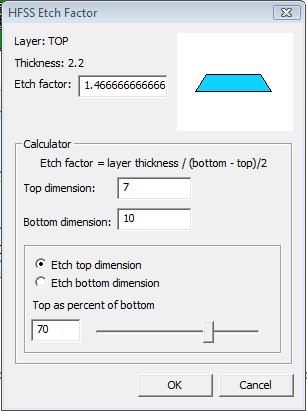


13 Assigning Variables Etching Factor 13

14 Huray Surface Roughness Model Improved surface roughness model for copper on laminates 14

15 Passivity Enforcement: Interpolating Sweeps Additional criteria to determine convergence Passivity violations used as new basis points Improves reliability of models in transient SPICE simulations 15

16 Frequency Dependant Materials 1. Multipole Debye Model Input This lets you provide the measured data of relative permittivity and loss tangent versus frequency. Based on this data the software dynamically generates frequency dependent expressions for relative permittivity and loss tangent. 2. Djordjevic-Sarkar Method HFSS allows you to enter the relative permittivity and loss tangent at a single measurement frequency. You may optionally enter the relative permittivity and conductivity at DC. This is the best method if you don t have measured data. 16
17 Distributed Solve Option (DSO) Problem is subdivided, and each subproblem is solved on a separate machine (including the Local Machine) Available distributions Parametric variable sweeps Frequency sweeps (HFSS) No limit to number of machines that may be used Same distributed analysis license works for Designer (Planar EM), ephysics, HFSS, Maxwell, and Q3D Extractor 17


18 Configuring the Machines Swept 8 variations from the 3 variables assigned to the models DSO using 9 Windows Server 2008 machines with 12 cores and 64 GB RAM each. Used 6 MP for each machine to have a total of 18 machines for the Frequency Sweep Used 6MP for Parametric Sweep 18

19 DSO Solution Times BGA End Frequency Sweep Nominal Project using DSO for the Frequency Sweep Adaptive Passes 55 mins Frequency Sweep 1 hour 46 mins WITHOUT DSO 16 hours 30mins Parametric Variations Solved 8 variations from the 3 variables available Cummulative Solve Time 72 hours 11 mins Longest Solve Time 12 hours 48 mins Time Savings 6.6X 19

20 DSO Solution Times Connector End Frequency Sweep Nominal Project using DSO for the Frequency Sweep Adaptive Passes 49 mins Frequency Sweep 3 hours 15 mins WITHOUT DSO 34 hours Parametric Variations Solved 8 variations from the 3 variables available Cummulative Solve Time 82 hours 43 mins Longest Solve Time 11 hours 9 mins Time Savings 7.4X 20

21 Using DSO with 2D Extractor for Long Transmission Lines For long uniform transmission lines, it is best to use a 2D field solution Same variables used for the transmission lines 21

22 Schematic Setup for Parametric Variations The 3 models are stitched together in schematic A parametric sweep is created that controls all 3 models 22
23 Parametric Sweep Results 0.00 XY Plot 4 Circuit1 ANSOFT Y Curve Info db(s(port1,port1)) LinearFrequency $brd_trace_w idth='3.2mil' $diel_thickness='3.6mil' $trace_etch='0' db(s(port1,port1)) LinearFrequency $brd_trace_w idth='4mil' $diel_thickness='3.6mil' $trace_etch='0' db(s(port1,port1)) LinearFrequency $brd_trace_w idth='3.2mil' $diel_thickness='4.6mil' $trace_etch='0' db(s(port1,port1)) LinearFrequency $brd_trace_w idth='4mil' $diel_thickness='4.6mil' $trace_etch='0' db(s(port1,port1)) LinearFrequency $brd_trace_w idth='3.2mil' $diel_thickness='3.6mil' $trace_etch='3' db(s(port1,port1)) LinearFrequency $brd_trace_w idth='4mil' $diel_thickness='3.6mil' $trace_etch='3' db(s(port1,port1)) LinearFrequency $brd_trace_w idth='3.2mil' $diel_thickness='4.6mil' $trace_etch='3' db(s(port1,port1)) LinearFrequency $brd_trace_w idth='4mil' $diel_thickness='4.6mil' $trace_etch='3' db(s(port1,port3)) LinearFrequency $brd_trace_w idth='3.2mil' $diel_thickness='3.6mil' $trace_etch='0' db(s(port1,port3)) F [GHz] 23
24 Conclusion We showed how Solver on Demand enables easier merging of complex geometries We showed how we can use IBIS AMI models to look at eye diagrams for the full channel We showed how manufacturing variations can be captured in the 3D model, and used in a parametric sweep in DesginerSI 24
Electromagnetics. R14 Update. Greg Pitner ANSYS, Inc. February 24, 2012
 Electromagnetics R14 Update Greg Pitner 1 HFSS Version 14 2 HFSS Overview Advanced Integrated Solver Technologies Finite Arrays with Domain Decomposition Hybrid solving: FEBI, IE Regions Physical Optics
Solving the challenges posed by Chip/Package/Board Co-Design
 Solving the challenges posed by Chip/Package/Board Co-Design Identify and locate sources of unwanted coupling Simulation link to EM: Critical Interconnect, Vias, Discontinuities, Embedded Passives, etc
HFSS 14 Update for SI and RF Applications Markus Kopp Product Manager, Electronics ANSYS, Inc.
 HFSS 14 Update for SI and RF Applications Markus Kopp Product Manager, Electronics ANSYS, Inc. 1 ANSYS, Inc. September 21, Advanced Solvers: Finite Arrays with DDM 2 ANSYS, Inc. September 21, Finite Arrays
HFSS Solver-On-Demand for Package and PCB Characterization Using Cadence Greg Pitner
 HFSS Solver-On-Demand for Package and PCB Characterization Using Cadence Greg Pitner 1 ANSYS, Inc. September 14, Problem Statement Usually SI engineers extract only the package or the pcb due to the trade-offs
HFSS Solver On Demand for Package and PCB Characterization Using Cadence. Greg Pitner
 HFSS Solver On Demand for Package and PCB Characterization Using Cadence Greg Pitner 1 Problem Statement Usually SI engineers extract only the package or the pcb due to the trade offs between capacity
Package on Board Simulation with 3-D Electromagnetic Simulation
 White Paper Package on Board Simulation with 3-D Electromagnetic Simulation For many years, designers have taken into account the effect of package parasitics in simulation, from using simple first-order
HFSS for ECAD: Package Modeling, MMIC and on-die extraction
 HFSS for ECAD: Package Modeling, MMIC and on-die extraction Alain Michel Technical Director, Europe 2010 ANSYS, Inc. All rights reserved. 1 ANSYS, Inc. Proprietary Agenda Introduction HFSS integrated Solver
Advanced SI Analysis Layout Driven Assembly. Tom MacDonald RF/SI Applications Engineer II
 Advanced SI Analysis Layout Driven Assembly 1 Tom MacDonald RF/SI Applications Engineer II Abstract As the voracious appetite for technology continually grows, so too does the need for fast turn around
Lecture 2: Introduction
 Lecture 2: Introduction v2015.0 Release ANSYS HFSS for Antenna Design 1 2015 ANSYS, Inc. Multiple Advanced Techniques Allow HFSS to Excel at a Wide Variety of Applications Platform Integration and RCS
HFSS 3D Components. Steve Rousselle, ANSYS. Build, Share, Conquer Release. Release ANSYS, Inc.
 HFSS 3D Components Build, Share, Conquer 2015.0 Release Steve Rousselle, ANSYS 1 2015 ANSYS, Inc. What is a 3D Component? Exploded View Assembly of 3D Components Device 2 2015 ANSYS, Inc. Introduction
HFSS 14 Update for SI and RF Applications. Presenter: Senior Application Engineer Jeff Tharp, Ph.D.
 HFSS 14 Update for SI and RF Applications Presenter: Senior Application Engineer Jeff Tharp, Ph.D. 1 Overview Advanced Integrated Solver Technologies Finite Arrays with Domain Decomposition Hybrid solving
A Modular Platform for Accurate Multi- Gigabit Serial Channel Validation
 A Modular Platform for Accurate Multi- Gigabit Serial Channel Validation Presenter: Andrew Byers Ansoft Corporation High Performance Electronics: Technical Challenges Faster data rates in increasingly
Genesys 2012 Tutorial - Using Momentum Analysis for Microwave Planar Circuits
 Genesys 2012 Tutorial - Using Momentum Analysis for Microwave Planar Circuits Create the following schematics in Figure 1 with Genesys s schematic editor, which depicts two sections of a cascaded microstrip
Pessimism removal in a system analysis of a 28Gbps SERDES link
 Pessimism removal in a system analysis of a 28Gbps SERDES link SERDES system modeling analysis from silicon macro to connector Olivier BAYET & Massimo Cereda, STMicroelectronics May 11 th 2016 from 9:50
HFSS Ansys ANSYS, Inc. All rights reserved. 1 ANSYS, Inc. Proprietary
 HFSS 12.0 Ansys 2009 ANSYS, Inc. All rights reserved. 1 ANSYS, Inc. Proprietary Comparison of HFSS 11 and HFSS 12 for JSF Antenna Model UHF blade antenna on Joint Strike Fighter Inherent improvements in
Board Design Guidelines for PCI Express Architecture
 Board Design Guidelines for PCI Express Architecture Cliff Lee Staff Engineer Intel Corporation Member, PCI Express Electrical and Card WGs The facts, techniques and applications presented by the following
SEAM-RA/SEAF-RA Series Final Inch Designs in PCI Express Applications Generation GT/s
 SEAM-RA/SEAF-RA Series Final Inch Designs in PCI Express Applications Generation 3-8.0 GT/s Copyrights and Trademarks Copyright 2011 Samtec, Inc. Developed in conjunction with Teraspeed Consulting Group
Using Sonnet in a Cadence Virtuoso Design Flow
 Using Sonnet in a Cadence Virtuoso Design Flow Purpose of this document: This document describes the Sonnet plug-in integration for the Cadence Virtuoso design flow, for silicon accurate EM modelling of
Powerful features (1)
") HFSS Overview Powerful features (1) Tangential Vector Finite Elements Provides only correct physical solutions with no spurious modes Transfinite Element Method Adaptive Meshing r E = t E γ i i ( x, y,
HFSS Overview Powerful features (1) Tangential Vector Finite Elements Provides only correct physical solutions with no spurious modes Transfinite Element Method Adaptive Meshing r E = t E γ i i ( x, y,
Optimization of Modern Memory
 System Design, Verificationand and Optimization of Modern Memory Interfaces (DDR3) Santa Clara, Aug 23 rd 2011 Robert Myoung Sr. Application Engineer 1 Agenda Introduction ECAD Geometry Translation SI/PI
ANSYS HFSS: Layout Driven Assembly in ANSYS Electronics Desktop
 Application Brief ANSYS HFSS: Layout Driven Assembly The ANSYS Electronics Desktop (AEDT) is an integrated environment with an easy-to-use interface that provides a streamlined workflow between ANSYS EM
Application Note. PCIE-EM Series Final Inch Designs in PCI Express Applications Generation GT/s
 PCIE-EM Series Final Inch Designs in PCI Express Applications Generation 3-8.0 GT/s Copyrights and Trademarks Copyright 2015, Inc. COPYRIGHTS, TRADEMARKS, and PATENTS Final Inch is a trademark of, Inc.
Electrical optimization and simulation of your PCB design
 Electrical optimization and simulation of your PCB design Steve Gascoigne Senior Consultant at Mentor Graphics Zagreb, 10. lipnja 2015. Copyright CADCAM Group 2015 The Challenge of Validating a Design..
FEKO Mesh Optimization Study of the EDGES Antenna Panels with Side Lips using a Wire Port and an Infinite Ground Plane
 FEKO Mesh Optimization Study of the EDGES Antenna Panels with Side Lips using a Wire Port and an Infinite Ground Plane Tom Mozdzen 12/08/2013 Summary This study evaluated adaptive mesh refinement in the
Application Note. PCIE-RA Series Final Inch Designs in PCI Express Applications Generation GT/s
 PCIE-RA Series Final Inch Designs in PCI Express Applications Generation 3-8.0 GT/s Copyrights and Trademarks Copyright 2012, Inc. COPYRIGHTS, TRADEMARKS, and PATENTS Final Inch is a trademark of, Inc.
Simulation Advances for RF, Microwave and Antenna Applications
 Simulation Advances for RF, Microwave and Antenna Applications Bill McGinn Application Engineer 1 Overview Advanced Integrated Solver Technologies Finite Arrays with Domain Decomposition Hybrid solving:
Vertical Conductive Structures
 Vertical Conductive Structures A new Interconnect Technique Agenda The need for an alternative PCB technology Introduction of VeCS Technology comparison Cost comparison State of VeCS technology Application
Simulation Strategies for Massively Parallel Supercomputer Design
 Simulation Strategies for Massively Parallel Supercomputer Design Authored by: Ansoft Corporation Special Thanks to: Cray Presentation #2 Ansoft 2003 / Global Seminars: Delivering Performance Introduction
Introduction to AWR Design Flow and New Features for V10
 Introduction to AWR Design Flow and New Features for V10 What s New In Version 10 imatch Matching Network Synthesis Matching Network Synthesis Tight integration with AWR tools Excellent starting point
CENG 4480 Lecture 11: PCB
 CENG 4480 Lecture 11: PCB Bei Yu Reference: Chapter 5 of Ground Planes and Layer Stacking High speed digital design by Johnson and Graham 1 Introduction What is a PCB Why we need one? For large scale production/repeatable
Construction of an electrical model of a TQFP100 package with IC-EMC
 Construction of an electrical model of a TQFP100 package with IC-EMC A. Boyer INSA-GEI, 135 Av de Rangueil 31077 Toulouse France Contact : alexandre.boyer@insa-toulouse.fr web site : www.ic-emc.org Abstract:
PCIEC PCI Express Jumper High Speed Designs in PCI Express Applications Generation GT/s
 PCIEC PCI Express Jumper High Speed Designs in PCI Express Applications Generation 3-8.0 GT/s Mated with PCIE-RA Series PCB Connectors Copyrights and Trademarks Copyright 2015, Inc. COPYRIGHTS, TRADEMARKS,
Laboratory Assignment: EM Numerical Modeling of a Stripline
 Laboratory Assignment: EM Numerical Modeling of a Stripline Names: Objective This laboratory experiment provides a hands-on tutorial for drafting up an electromagnetic structure (a stripline transmission
CECOS University Department of Electrical Engineering. Wave Propagation and Antennas LAB # 1
 CECOS University Department of Electrical Engineering Wave Propagation and Antennas LAB # 1 Introduction to HFSS 3D Modeling, Properties, Commands & Attributes Lab Instructor: Amjad Iqbal 1. What is HFSS?
Outline. Darren Wang ADS Momentum P2
 Outline Momentum Basics: Microstrip Meander Line Momentum RF Mode: RFIC Launch Designing with Momentum: Via Fed Patch Antenna Momentum Techniques: 3dB Splitter Look-alike Momentum Optimization: 3 GHz Band
Keysight EEsof EDA Planar Electromagnetic (EM) Simulation in ADS. Demo Guide
 Simulation in ADS. Demo Guide") Keysight EEsof EDA Planar Electromagnetic (EM) Simulation in ADS Demo Guide 02 Keysight Planar Electromagnetic (EM) Simulation in ADS - Demo Guide Keysight ADS provides two key electromagnetic simulators
Keysight EEsof EDA Planar Electromagnetic (EM) Simulation in ADS Demo Guide 02 Keysight Planar Electromagnetic (EM) Simulation in ADS - Demo Guide Keysight ADS provides two key electromagnetic simulators
Design Guidelines for 100 Gbps - CFP2 Interface
 2014.01.16 AN-684 Subscribe This document shows an example layout design that implements a 4 x 25/28 Gbps CFP2 module interface that meets the insertion and return loss mask requirements proposed in the
Workshop 3-1: Coax-Microstrip Transition
 Workshop 3-1: Coax-Microstrip Transition 2015.0 Release Introduction to ANSYS HFSS 1 2015 ANSYS, Inc. Example Coax to Microstrip Transition Analysis of a Microstrip Transmission Line with SMA Edge Connector
Additional Trace Losses due to Glass- Weave Periodic Loading. Jason R. Miller, Gustavo Blando and Istvan Novak Sun Microsystems
 Additional Trace Losses due to Glass- Weave Periodic Loading Jason R. Miller, Gustavo Blando and Istvan Novak Sun Microsystems 1 Introduction PCB laminates are composed of resin and a glass fabric Two
First Steps with ADS and Coax Modeling
 First Steps with ADS and Coax Modeling ADS Session 1 Start ADS and Create an Empty Project Look for a desktop icon or start menu item entitled Advanced Design System 2009 ADS will start up and you will
What s New in HyperLynx 8.0
 What s New in HyperLynx 8.0 Copyright Mentor Graphics Corporation 2009 All Rights Reserved. Mentor Graphics, Board Station XE Flow, ViewDraw, Falcon Framework, IdeaStation, ICX and Tau are registered trademarks
EXAMINING THE IMPACT OF SPLIT PLANES ON SIGNAL AND POWER INTEGRITY
 EXAMINING THE IMPACT OF SPLIT PLANES ON SIGNAL AND POWER INTEGRITY Jason R. Miller, Gustavo J. Blando, Roger Dame, K. Barry A. Williams and Istvan Novak Sun Microsystems, Burlington, MA 1 AGENDA Introduction
Modeling of Connector to PCB Interfaces. CST User Group Meeting, September 14, 2007 Thomas Gneiting, AdMOS GmbH
 Modeling of Connector to PCB Interfaces CST User Group Meeting, September 14, 2007 Thomas Gneiting, AdMOS GmbH thomas.gneiting@admos.de Table of Content Introduction Parametric CST model of connector to
QUEST 3D RLCG Extraction Depending on Frequency. RF Structures Parasitic Extractor
 QUEST 3D RLCG Extraction Depending on Frequency RF Structures Parasitic Extractor Introduction Type of Simulation Inputs / Outputs Graphical Interface Technology Process Layout Field Solver Output DOE
Addressing the Power-Aware Challenges of Memory Interface Designs
 Addressing the Power-Aware Challenges of Memory Interface Designs One of the toughest challenges in designing memory interfaces is accurately measuring timing while also considering fluctuations in power
Ansys Designer RF Training Lecture 2: Introduction to the Designer GUI
 Ansys Designer RF Solutions for RF/Microwave Component and System Design 7. 0 Release Ansys Designer RF Training Lecture 2: Introduction to the Designer GUI Ansoft Designer Desktop Menu bar Toolbars Schematic
ECE ILLINOIS. ECE 451: Ansys HFSS Tutorial. Simulate and Analyze an Example of Microstrip Line. Drew Handler, Jerry Yang October 20, 2014
 ECE ILLINOIS ECE 451: Ansys HFSS Tutorial Simulate and Analyze an Example of Microstrip Line Drew Handler, Jerry Yang October 20, 2014 Introduction ANSYS HFSS is an industry standard tool for simulating
LAB # 2 3D Modeling, Properties Commands & Attributes
 COMSATS Institute of Information Technology Electrical Engineering Department (Islamabad Campus) LAB # 2 3D Modeling, Properties Commands & Attributes Designed by Syed Muzahir Abbas 1 1. Overview of the
Customer Training Material. Segmented Return Path. ANSYS Q3D Extractor. ANSYS, Inc. Proprietary 2011 ANSYS, Inc. All rights reserved. WS1.
 Workshop 1.3 Segmented Return Path Introduction to ANSYS Q3D Extractor WS1.3-1 Example Segmented Return Path Segmented Return Path This example is intended to show you how to create, simulate, and analyze
An Innovative Simulation Workflow for Debugging High-Speed Digital Designs using Jitter Separation
 An Innovative Simulation Workflow for Debugging High-Speed Digital Designs using Jitter Separation C. Chastang, A. Amédéo V. Poisson, P. Grison, F. Demuynck C. Gautier, F. Costa Thales Communications &
Layer Stackup Wizard: Intuitive Pre-Layout Design
 Application Brief Layer Stackup Wizard: Intuitive Pre-Layout Design INTRODUCTION This Application Brief describes the Layer Stackup Wizard, a powerful utility within ANSYS SIwave for pre-layout stackup
HFSS Hybrid Finite Element and Integral Equation Solver for Large Scale Electromagnetic Design and Simulation
 HFSS Hybrid Finite Element and Integral Equation Solver for Large Scale Electromagnetic Design and Simulation Laila Salman, PhD Technical Services Specialist laila.salman@ansys.com 1 Agenda Overview of
A Crash Course on Using Agilent Advanced Design System (ADS)
") A Crash Course on Using Agilent Advanced Design System (ADS) By Chris Sanabria, sanabria@ece.ucsb.edu 2/9/02 If you are an engineer and have anything to do with circuit simulation, in particular high frequency
A Crash Course on Using Agilent Advanced Design System (ADS) By Chris Sanabria, sanabria@ece.ucsb.edu 2/9/02 If you are an engineer and have anything to do with circuit simulation, in particular high frequency
Welcome. Joe Civello ADS Product Manager Agilent Technologies
 Welcome Joe Civello ADS Product Manager Agilent Technologies Agilent Technologies 2011 Agenda RF & microwave market trends & how Agilent EEsof is investing its R&D Multi-technology design with ADS 2011
I N T E R C O N N E C T A P P L I C A T I O N N O T E. STRADA Whisper 4.5mm Connector Enhanced Backplane and Daughtercard Footprint Routing Guide
 I N T E R C O N N E C T A P P L I C A T I O N N O T E STRADA Whisper 4.5mm Connector Enhanced Backplane and Daughtercard Footprint Routing Guide Report # 32GC001 01/26/2015 Rev 3.0 STRADA Whisper Connector
Workshop 5-1: Dynamic Link
 Workshop 5-1: Dynamic Link 2015.0 Release ANSYS HFSS for Antenna Design 1 2015 ANSYS, Inc. Overview Linear Circuit Overview Dynamic Link Push Excitations Dynamic Link Example: Impedance Matching of Log-Periodic
2010 ANSYS, Inc. All rights reserved. 1 ANSYS, Inc. Proprietary
 Bi-directional Automatic Electromagnetic-Thermal Coupling for HEV/EV Traction Motor Design Using Maxwell and ANSYS Mechanical Peng Yuan Eric Lin Zed (Zhangjun) Tang ANSYS, Inc. 2010 ANSYS, Inc. All rights
As Dave Dunham from Molex Corp. likes to say, "When designing highspeed serial links beyond 10 GB/s, everything matters".
 1 As Dave Dunham from Molex Corp. likes to say, "When designing highspeed serial links beyond 10 GB/s, everything matters". 2 And part of that everything is accurate modeling of transmission line losses.
Overview. Ansoft High Frequency Structure Simulator v 9.0 Training Seminar 1
 Ansoft High Frequency Structure Simulator v 9.0 Training Seminar 1 The Process Design Solution Type 1.1. Boundaries 1. Parametric Model Geometry/Materials 2. Analysis Solution Setup Frequency Sweep 1.2.
Allegro Sigrity SI Streamlining the creation of high-speed interconnect on digital PCBs and IC packages
 Streamlining the creation of high-speed interconnect on digital PCBs and IC packages The Cadence Allegro Sigrity signal integrity (SI) integrated high-speed design and analysis environment streamlines
Cadence Virtuoso Schematic Design and Circuit Simulation Tutorial
 Cadence Virtuoso Schematic Design and Circuit Simulation Tutorial Introduction This tutorial is an introduction to schematic capture and circuit simulation for ENGN1600 using Cadence Virtuoso. These courses
HFSS - Antennas, Arrays and FSS's. David Perry Applications Engineer Ansoft Corporation
 HFSS - Antennas, Arrays and FSS's David Perry Applications Engineer Ansoft Corporation Synopsis Some Excerpts from What s New Enhancements to HFSS Wave Guide Simulator (WGS) What is it? Why you would use
Getting Started with Q3D Extractor A 3D PCB Via Model
 Getting Started with Q3D Extractor A 3D PCB Via Model ANSYS, Inc. 275 Technology Drive Canonsburg, PA 15317 USA Tel: (+1) 724-746-3304 Fax: (+1) 724-514-9494 General Information: AnsoftInfo@ansys.com Technical
Microwave Office Training
 Microwave Office Training Schematic Layout Schematic Layout Schematic View Circuit We are Here! Schematic Layout View External World Need Export Mapping Two views of the same circuit! - including connectivity
Integrating ADS into a High Speed Package Design Process
 Integrating ADS into a High Speed Package Design Process Page 1 Group/Presentation Title Agilent Restricted Month ##, 200X Agenda High Speed SERDES Package Design Requirements Performance Factor and Design
Complete PCB Design Using OrCad Capture and Layout
 Complete PCB Design Using OrCad Capture and Layout By Kraig Mitzner Amsterdam Boston Heidelberg London New York Oxford Paris San Diego San Francisco Singapore Sydney Tokyo Newnes is an imprint of Elsevier
Optimum Placement of Decoupling Capacitors on Packages and Printed Circuit Boards Under the Guidance of Electromagnetic Field Simulation
 Optimum Placement of Decoupling Capacitors on Packages and Printed Circuit Boards Under the Guidance of Electromagnetic Field Simulation Yuzhe Chen, Zhaoqing Chen and Jiayuan Fang Department of Electrical
Modern Memory Interfaces (DDR3) Design with ANSYS Virtual Prototype approach
 Design with ANSYS Virtual Prototype approach") Modern Memory Interfaces (DDR3) Design with ANSYS Virtual Prototype approach 1 ANSYS, Inc. Proprietary 2012 ANSYS, Inc. November 14, 2012 1-1 Agenda DDR Design Challenges How does simulation solve these
Modern Memory Interfaces (DDR3) Design with ANSYS Virtual Prototype approach 1 ANSYS, Inc. Proprietary 2012 ANSYS, Inc. November 14, 2012 1-1 Agenda DDR Design Challenges How does simulation solve these
Design and Characterization of a Two Channel Transmitter SiP Module
 Design and Characterization of a Two Channel Transmitter SiP Module Amkor Technology: Nozad Karim, Rong Zhou, Ozgur Misman, Mike DeVita, Yida Zou Contact: Nozad Karim, Ph: 480 786 7731, email: Nozad.Karim@amkor.com
Applying the Cannonball Stack Principle to the Huray Roughness Model in Polar Si9000e
 Applying the Cannonball Stack Principle to the Huray Roughness Model in Polar Si9000e In addition to the Hammerstad and Groisse models for predicting the additional attenuation due to surface roughness,
m/matl - The EM Technology File Editor for RFIC
 m/matl - The EM Technology File Editor for RFIC Table of contents: m/matl - The EM Technology File Editor for RFIC... 1 1. Introduction... 2 2. What file formats and design flows are supported?... 2 Read
AXIEM EM Simulation/Verification of a Cadence Allegro PCB
 Application Example AXIEM EM Simulation/Verification of a Cadence Allegro PCB Overview This application example outlines the electromagnetic (EM) simulation and verification flow that exists between Cadence
Design Process and Technical Thoughts on a Two Channel PHY Approach
 Design Process and Technical Thoughts on a Two Channel PHY Approach Joel Goergen Cisco, Beth Kochuparambil Cisco IEEE 802.3bj January 2012 Interim, Newport Beach, CA, USA Supporters Howard Frazier Broadcom
Introduction to ANSYS DesignXplorer
 Overview 14. 5 Release Introduction to ANSYS DesignXplorer 1 2013 ANSYS, Inc. September 27, 2013 What is DesignXplorer? DesignXplorer (DX) is a tool that uses response surfaces and direct optimization
End Launch Connector Series. Introduction Specifications Model Numbers Installation Procedures... 63
 End Launch Connector Series Index End Launch Connectors (to 50 GHz).... Page Introduction... 60 Specifications... 61 Model Numbers... 62 Installation Procedures... 63 Test Data (Grounded Coplanar)... 64
Simulation Advances. Antenna Applications
 Simulation Advances for RF, Microwave and Antenna Applications Presented by Martin Vogel, PhD Application Engineer 1 Overview Advanced Integrated Solver Technologies Finite Arrays with Domain Decomposition
Realize Your Product Promise. DesignerRF
 Realize Your Product Promise DesignerRF Four-element antenna array showing current distribution and far-field gain, created in DesignerRF using layout editor and solved via HFSS with Solver on Demand technology
MDI for 4x25G Copper and Fiber Optic IO. Quadra (CFP4 proposal) Connector System
 Connector System") MDI for 4x25G Copper and Fiber Optic IO Quadra (CFP4 proposal) Connector System Nov 7, 2011 Nathan Tracy, TE Connectivity Tom Palkert, Molex 4x25Gb/s MDI Potential Requirements Critical Needs: Excellent
MDI for 4x25G Copper and Fiber Optic IO Quadra (CFP4 proposal) Connector System Nov 7, 2011 Nathan Tracy, TE Connectivity Tom Palkert, Molex 4x25Gb/s MDI Potential Requirements Critical Needs: Excellent
Workshop 3: Basic Electrostatic Analysis. ANSYS Maxwell 2D V ANSYS, Inc. May 21, Release 14.5
 Workshop 3: Basic Electrostatic Analysis ANSYS Maxwell 2D V16 2013 ANSYS, Inc. May 21, 2013 1 Release 14.5 About Workshop Introduction on the Electrostatic Solver This workshop introduces the Electro Static
Index. End Launch Connector Series. End Launch Connectors (67 GHz)... Page. Installation Procedure End Launch Connector Dimensions...
... Page. Installation Procedure End Launch Connector Dimensions...") Connector Series Index (67 GHz).... Page Specifications... 51 Introduction... 52 Procedure... 53 Connector Dimensions... 54 Connector Numbers... 55 Typical Test Data... 56 50 Specifications Applications
Connector Series Index (67 GHz).... Page Specifications... 51 Introduction... 52 Procedure... 53 Connector Dimensions... 54 Connector Numbers... 55 Typical Test Data... 56 50 Specifications Applications
Advances in Measurement Based Transient Simulation
 Time Domain Simulation in ADS, Slide - 1 Advances in Measurement Based Transient Simulation Presented by GigaTest Labs Gary Otonari and Orlando Bell March, 2008 1 Time Domain Simulation in ADS, Slide -
CADSTAR. Jeroen Leinders CADSTAR Distribution Manager. Zuken
 CADSTAR Jeroen Leinders CADSTAR Distribution Manager 1 Introduction I m the CADSTAR distribution manager for Zuken managing approximately 30 resellers worldwide, based out of my home office in the Netherlands.
TQPED MMIC Design Training
 TQPED MMIC Design Training Outline Installation and Use of the Library AWR AWR Design Kit (PDK Process Design Kit) ICED Layout Kit Create a new document using the Library Environment Setup Hotkeys Background
RF/Microwave Circuits I Laboratory #2. Circuit Tuning and EM Simulation with Momentum
 RF/Microwave Circuits I Laboratory #2 Circuit Tuning and EM Simulation with Momentum Overview This laboratory continues the basic ADS training approach from Laboratory #1. The two main objectives for this
Chip/Package/Board Design Flow
 Chip/Package/Board Design Flow EM Simulation Advances in ADS 2011.10 1 EM Simulation Advances in ADS2011.10 Agilent EEsof Chip/Package/Board Design Flow 2 RF Chip/Package/Board Design Industry Trends Increasing
A Proposal for Developing S2IBISv3
 A Proposal for Developing S2IBISv3 Paul Franzon Michael Steer Automated Design Tools for Integrated Mixed Signal Microsystems (NeoCAD) Outline Background DARPA Program NeoCad Program Objectives Program
Chapter 4 Determining Cell Size
 Chapter 4 Determining Cell Size Chapter 4 Determining Cell Size The third tutorial is designed to give you a demonstration in using the Cell Size Calculator to obtain the optimal cell size for your circuit
AMI Applications in High-speed Serial Channel Analysis and Measurement Correlation
 AMI Applications in High-speed Serial Channel Analysis and Measurement Correlation Jia Wei, Sunanbing, Zhu ShunLin Jia.wei@zte.com.cn, sun.anbing@zte.com.cn, Zhu.shunlin@zte.com.cn High-Speed System Lab,ZTE
O N C A D E N C E V I R T U O S O. CHEN, Jason Application Engineer, Keysight Technologies
 O N C A D E N C E V I R T U O S O CHEN, Jason 2018.05.08 Application Engineer, Keysight Technologies Introduction to Momentum Momentum Features for RFIC Design Circuit/EM Cosimulation Flow on Cadence Virtuoso
A Practical Methodology for SerDes Design
 A Practical Methodology for SerDes Design Asian IBIS Summit, Shanghai, China, November 14, 2018 Authors: Amy Zhang, Guohua Wang, David Zhang, Zilwan Mahmod, Anders Ekholm agenda Challenges in Traditional
Revision Notes: July2004 Generate tutorial for single transistor analysis. Based on existing schematic entry tutorial developed for ECE410
 Cadence Analog Tutorial 1: Schematic Entry and Transistor Characterization Created for the MSU VLSI program by Professor A. Mason and the AMSaC lab group. Revision Notes: July2004 Generate tutorial for
3D EM Simulation in the Design Flow of High-Speed Multi-Pin Connectors
 3D EM Simulation in the Design Flow of High-Speed Multi-Pin Connectors Application and Simulation courtesy of Thomas Gneiting, AdMOS GmbH, Frickenhausen, Germany. This article describes the design flow
Maxwell v Example (2D/3D Transient) Core Loss. Transformer Core Loss Calculation in Maxwell 2D and 3D
 Core Loss. Transformer Core Loss Calculation in Maxwell 2D and 3D") Transformer Core Loss Calculation in Maxwell 2D and 3D This example analyzes cores losses for a 3ph power transformer having a laminated steel core using Maxwell 2D and 3D. The transformer is rated 115-13.8kV,
Transformer Core Loss Calculation in Maxwell 2D and 3D This example analyzes cores losses for a 3ph power transformer having a laminated steel core using Maxwell 2D and 3D. The transformer is rated 115-13.8kV,
March 4-7, 2018 Hilton Phoenix / Mesa Hotel Mesa, Arizona Archive
 March 4-7, 2018 Hilton Phoenix / Mesa Hotel Mesa, Arizona Archive 2018 BiTS Workshop Image: pilgrims49 / istock COPYRIGHT NOTICE The presentation(s)/poster(s) in this publication comprise the Proceedings
High Speed and High Power Connector Design
 High Speed and High Power Connector Design Taiwan User Conference 2014 Introduction High speed connector: Electrically small Using differential signaling Data rate >100Mbps High power connector: Static
Obsolete Parameter Conditions Minimum Typical Maximum Units
 Product Description The PE4242 UltraCMOS RF Switch is designed to cover a broad range of applications from 1 MHz through 3 GHz. This reflective switch integrates on-board CMOS control logic with a low
Lecture 7: Introduction to HFSS-IE
 Lecture 7: Introduction to HFSS-IE 2015.0 Release ANSYS HFSS for Antenna Design 1 2015 ANSYS, Inc. HFSS-IE: Integral Equation Solver Introduction HFSS-IE: Technology An Integral Equation solver technology
EDA365. DesignCon Impact of Backplane Connector Pin Field on Trace Impedance and Vertical Field Crosstalk
 DesignCon 2007 Impact of Backplane Connector Pin Field on Trace Impedance and Vertical Field Crosstalk Ravi Kollipara, Rambus, Inc. ravik@rambus.com, (650) 947-5298 Ben Chia, Rambus, Inc. Dan Oh, Rambus,
Cadence Power Integrity Solutions For PCBs and IC Packages. May 2013
 Cadence Power Integrity Solutions For PCBs and IC Packages May 2013 Simultaneous Switching Noise (SSN) A Power Integrity Issue Design with decaps intentionally removed to demonstrate how poor PI performance
Release Notes Version 5
 Release Notes Version 5 Version 5.1 (2017-01-31) Solder Joint Fatigue Calculix Support for Column Grid Array (CGA) modeling for Solder Joint Fatigue FEA analysis and the Solder Fatigue tool has been added