Vertical Conductive Structures
|
|
|
- Arthur Shelton
- 6 years ago
- Views:
Transcription
1 Vertical Conductive Structures A new Interconnect Technique
2 Agenda The need for an alternative PCB technology Introduction of VeCS Technology comparison Cost comparison State of VeCS technology Application notes Transparent layer transition
3 The need for an alternative PCB technology


4 Grid arrays driving complexity Source: Ravi Mahajan, Intel Corporation


5 Limitation of current technology Sub 1.0mm pitch BGA type packages are difficult to route. Layer counts are going up High speed signals require point to point routing requiring extra layers. High speed is analogue to power hungry applications. Side view of routing channels

6 Limitation of current technology Current routing channels has limited capability below 1.0mm pitch Power planes are cut up reducing efficiency. No signal reference due to cut up planes.


7 PCB technology legging behind Through hole technology is limited and take to much space. Holes cannot be placed closer. Sequential build-ups are a good but expensive solution. Yield is dropping when complexity increases.

8 Slow down of smaller pitch packages Trend towards 0.8mm for Data/Tele-com and computing Routing channel is becoming to small to rout (differential) 0,1mm track and gap. Power distribution into core of package is difficult and expensive. Many heavy copper planes required. Conclusion : PCB Technology is not keeping up with package trends PCB s prices will rise due layer count increase, Sequential builds to yield loss and Push for package complexity
9 Introduction to VeCS


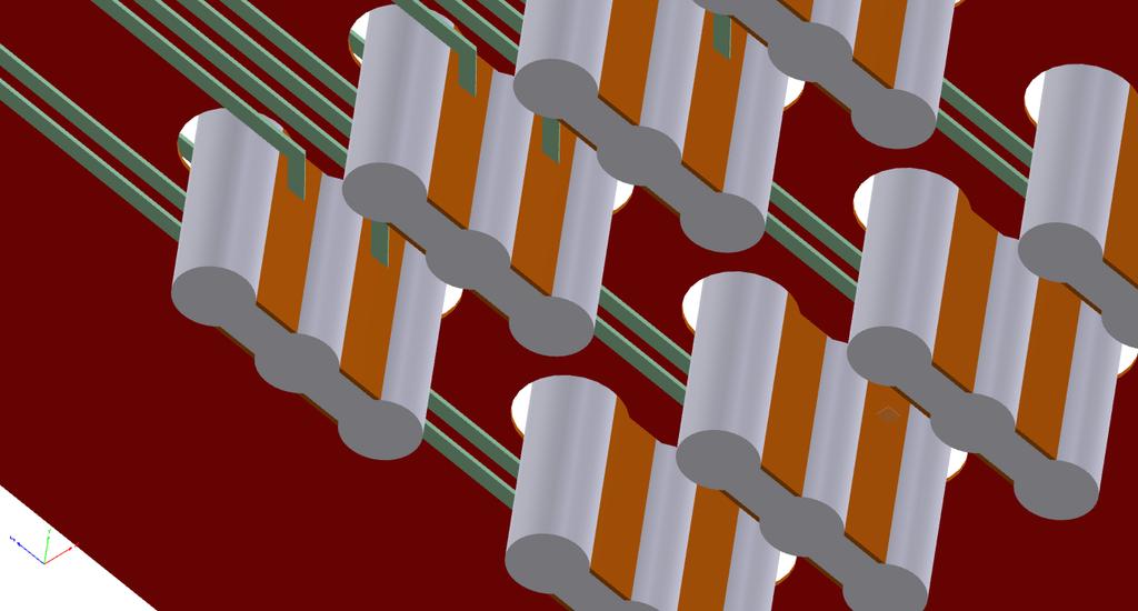
10 What is VeCS VeCS stands for Vertical Conductive Structure A traditional through hole or blind hole is too big and too disturbing in terms of SI. VCS creates a higher density of connections to the internal layers and with less distortion of the signal. Less cutting in the power & ground planes for a better current carrying capacity and better reference plane for the striplines. VeCS is patent pending and can be licensed via NextGIn technologies. The technology can be build by any medium to advanced board shop after training and licensing. No direct new capital equipment is required.

11 VeCS Principles The hole is replaced by a vertical trace or half a sphere. Preferred is the vertical trace from a signal integrity performance. Structure can be filled and over-plated depending application Example Pin-assignment Signal PWR/GND More vertical connections per surface area No CAF path between vertical traces Coupling and Broad side coupling Thicker dielectrics, wider traces PWR/GND Signal Signal Signal PWR/GND Signal

12 VeCS and routability VeCS uses special formed cavities that can connect to multiple internal layers using less space then vias or microvias resulting in wider router channels under Area Array Components like BGA s
13 VeCS and routability

14 Traditional channels disappears


15 VeCS effect on planes Planes are becoming more and more important, traditional planes under BGA are cut up to small slivers of copper. Example shows a plane under a 0.7mm pitch BGA with VeCS. A much more solid plane and reference compared to traditional via technology.
16 Technology Comparison VeCS vs. conventionial through hole

17 VeCS in design 0.8mm array VeCS slot BGA pad Routing channel width is twice the device pitch.

18 Diagonal slot placement Increase of routing channel by 2x Sqrt(2). 1,0mm = 2,82mm 0,5mm = 1,41mm pad size More signals per channel or more spaces between traces. More solid power/gnd copper into the packages.

19 Diagonal slot placement BGA pad 2nd drill Plated slot
20 Routing-channel utilization
21 VeCS-2 or High Aspect Ration Blind Structures (HARB)

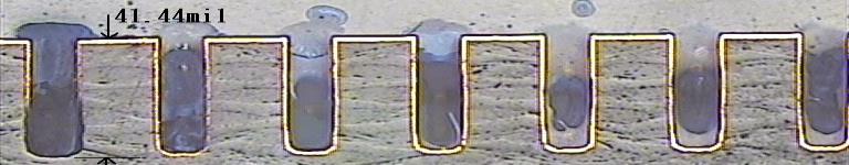
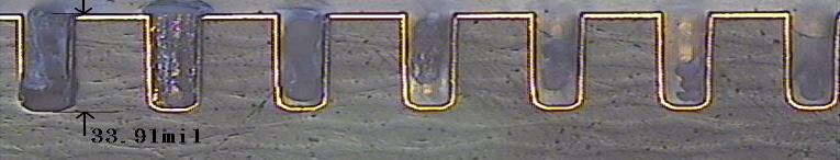
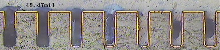
22 Plating results blind structures Shorter slot length reduce the plating capability.
 and ground for power hungry applications. Stubless connection to internal layers.")
23 What can you do with VeCS-2 Separate circuits on top and bottom increase density and Utilize routing space much better, no via penetration through the board. (no sequential lamination required). Create connections for power(s) and ground for power hungry applications. Stubless connection to internal layers. Avoid sequential built-ups Group rou ng top components Rou ng Between groups Group rou ng Bo om components


24 VeCS-2 application Blockage free routing under the VeCS element. No backdrilling required stublength of ± 8 mil. VeCS-2 element can be stretched, bent, etc.


25 BGA fanout Slot depths step down to each layer creating a wide routing channel.
26 Application Notes NextGIn technologies Connection to the Next Level
27 VeCS stackup configurations Traditional, VeCS-1, slot going all the way through the board. VeCS-1 buried and capped using Microvias as the connection to the out-side. VeCS-2, slots to certain depths combined with a through slot. This can be buried as well in combination with Microvias. VeCS-2 slots can be applied from both sides.


28 BGA fanout using VeCS-2 The middle part (conductive material is removed to create two different potentials two the left and right of the slot. Not every position in the slot need to be processed in this way. It dependents on the design Top view of VeCS-2 slot showing multiple depths and a section going through the board.

29 Intel Xeon E7 Footprint Example of the Intel Xeon E7 footprint The pads are arrange in an equal pattern of 40 mils as shown below. 0,4mm 40mil 40mil

30 VeCS fanout of Intel Xeon E7 This example shows a possible VeCS fan-out of the Intel Xeon E7 footprint. The track and gap is 0,1mm, there are 14 lines per VeCS channel. Many other VeCS patterns are possible, one example is given in this document.
 Slot length (variable) 0,3mm 2nd rout 0,35mm 0,25mm Ver tical trace")
31 0,35mm staggered VeCS fanout VeCS slots are buried and connected using Microvia on two sides. 0,5mm 0,35mm Plated slot, (not filled) Slot length (variable) 0,3mm 2nd rout 0,35mm 0,25mm Ver tical trace width: 0,1mm
 routed either with 2 traces of 0,12mm and")

32 0,35mm staggered VeCS fanout A high dense BGA (578 I/O) routed either with 2 traces of 0,12mm and 0,12mm gaps or a 3 traces of 0,08mm and 0,08mm gap Layer 2/Ln-1, microvia landing pads Slot layer Signal layer
, banks are all differential as well.")
33 Fan-out of Xilinx FLGA 2892 Fan-out using VeCS-2 of the 54x54, 1.0mm pitch BGA from Xilinx FLGA 2892 High speed SERDES (differential lines), banks are all differential as well. Uncoloured squares are all power / GND pins.
 Vias Different depths of")
34 Fan-out of Xilinx FLGA 2892 Fan-out of Xilinx FLGA2892, BGA 1,0mm, array 54x54 Through hole (standard) Vias Different depths of VeCS-2

35 Fan-out of Xilinx FLGA 2892 High Speed SERDES channels can be routed with wider traces then a traditional channel. Trace on lower layers (green) can be routed without any blockages.

36 Fan-out of Xilinx FLGA 2892 Differential routing using VeCS-2 Different slot depths in different colours

37 Fan-out example(s) Fan-out of Xilinx FLGA2892, BGA 1,0mm array 54x54 Non-blockage routing when using blind technology. Traces cross over (below) slots.
38 Fan-out 1,0 mm pitch BGA Through hole + backdrill design rule 1,0mm Diff. pair VeCS design rule 2,0 mm 1,3 mm 0,5 mm 1,0mm 0,25 mm 2x 0,1 mm 3x 0,1 mm Back drill 0,4 mm 0,25 mm 1,0mm 3x 0,1 mm 0,3 mm 0,3 mm 0,5 mm 2x 0,1 mm 3x 0,1 mm
39 Cost Comparison
40 Cost comparison The cost reduction is realized by reducing the layer count of the board ie. making more efficient use of the routing space Price index Through hole vs. VeCS Cost reduction 35% 24 layer Through hole 14 layer VeCS In this example a 24 layer is reduced to 14 layers realizing a cost reduction of 35% The same bandwidth of reductions can be applied for other layer count and constructions.

 VOH:")

41 Cost comparison in detail Legenda BOM: Bill of Materials (direct materials) SUP: Supplies (indriect materials) VOH: Variable OverHead FOH: Fixed OverHead layer 0 Through hole VeCS 14 layer
42 State of VeCS technology


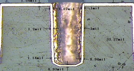
43 Initial results from Proof Of Concept Top view after plate second drill, Cavity size 0,3mm, 2 nd drill diameter 0,6 mm Cross section showing two sides of cavity Cross section showing Vertical conductive structure

44 Manufacturing Examples 12 Layer Test Board, 2.2 mm thick, Megtron 6 0.5mm, 0.75mm, 0.8mm and 1.0mm BGA on a single panel Test vehicles are exposed to 6x reflow at 288 degree Celcius, not deviations found after cross section.


45 Examples after solder shock (6x)
46 VeCS Signal Integrity performance


47 TDR measurements first prototype SMA connector forhigh frequency BGA area with VeCS


48 Transparant layer transition Objective: Create a non-reflective layer transition in order to re-introduce Via/VeCS-stitching to minimize point to point topology. Top side back routed Plated slot 2 nd route Differential pair SMA connector forhigh frequency


49 Transparant layer transition Vertical traces of the differential pair. Anti-pad Top view The VeCS model is created in Simbeor for Si simulations
50 Transparant layer transition Inductive Capacitive TDR response shows simulations for different trace widths and anti-pad sizes going from Capacitive to Inductive. The VeCS-2 element we can tune close to a transparent, non reflective element. Simulations made using Simbeor


51 Transparant layer transition Eye-diagram simulation at 30Gb/S Eye diagram of launch signal Eye diagram of exit signal

52 Transparant layer transition Input and output eye-diagrams superimposed. The (red) eye is just slight smaller then the input diagram.
53 NextGIn technologies Address details: Connection to the Next Level NextGIn technology BV Schrevenhofdreef RM Helmond The Netherlands Contactperson: Joan Tourné Telephone : info@nextgin-tech.com
I N T E R C O N N E C T A P P L I C A T I O N N O T E. STEP-Z Connector Routing. Report # 26GC001-1 February 20, 2006 v1.0
 I N T E R C O N N E C T A P P L I C A T I O N N O T E STEP-Z Connector Routing Report # 26GC001-1 February 20, 2006 v1.0 STEP-Z CONNECTOR FAMILY Copyright 2006 Tyco Electronics Corporation, Harrisburg,
I N T E R C O N N E C T A P P L I C A T I O N N O T E. Z-PACK TinMan Connector Routing. Report # 27GC001-1 May 9 th, 2007 v1.0
 I N T E R C O N N E C T A P P L I C A T I O N N O T E Z-PACK TinMan Connector Routing Report # 27GC001-1 May 9 th, 2007 v1.0 Z-PACK TinMan Connectors Copyright 2007 Tyco Electronics Corporation, Harrisburg,
I N T E R C O N N E C T A P P L I C A T I O N N O T E. STRADA Whisper 4.5mm Connector Enhanced Backplane and Daughtercard Footprint Routing Guide
 I N T E R C O N N E C T A P P L I C A T I O N N O T E STRADA Whisper 4.5mm Connector Enhanced Backplane and Daughtercard Footprint Routing Guide Report # 32GC001 01/26/2015 Rev 3.0 STRADA Whisper Connector
I N T E R C O N N E C T A P P L I C A T I O N N O T E. Advanced Mezzanine Card (AMC) Connector Routing. Report # 26GC011-1 September 21 st, 2006 v1.
 Connector Routing. Report # 26GC011-1 September 21 st, 2006 v1.") I N T E R C O N N E C T A P P L I C A T I O N N O T E Advanced Mezzanine Card (AMC) Connector Routing Report # 26GC011-1 September 21 st, 2006 v1.0 Advanced Mezzanine Card (AMC) Connector Copyright 2006
I N T E R C O N N E C T A P P L I C A T I O N N O T E Advanced Mezzanine Card (AMC) Connector Routing Report # 26GC011-1 September 21 st, 2006 v1.0 Advanced Mezzanine Card (AMC) Connector Copyright 2006
BGA Fanout Patterns. Charles Pfeil. Engineering Director Systems Design Division
 BGA Fanout Patterns Charles Pfeil Engineering Director Systems Design Division IPC Irvine Charles Pfeil Background 1966-1987 PCB Designer 1978-1987 Founder of Computer Circuits Inc., Fairfax VA, PCB Design
Board Design Guidelines for PCI Express Architecture
 Board Design Guidelines for PCI Express Architecture Cliff Lee Staff Engineer Intel Corporation Member, PCI Express Electrical and Card WGs The facts, techniques and applications presented by the following
EDA365. DesignCon Impact of Backplane Connector Pin Field on Trace Impedance and Vertical Field Crosstalk
 DesignCon 2007 Impact of Backplane Connector Pin Field on Trace Impedance and Vertical Field Crosstalk Ravi Kollipara, Rambus, Inc. ravik@rambus.com, (650) 947-5298 Ben Chia, Rambus, Inc. Dan Oh, Rambus,
Lab 9 PCB Design & Layout
 Lab 9 PCB Design & Layout ECT 224L Department of Engineering Technology Lab 9 PCB Traces Size dependent upon electrical requirements, design constraints (routing space and clearance), and trace/space resolution
Complete PCB Design Using OrCad Capture and Layout
 Complete PCB Design Using OrCad Capture and Layout By Kraig Mitzner Amsterdam Boston Heidelberg London New York Oxford Paris San Diego San Francisco Singapore Sydney Tokyo Newnes is an imprint of Elsevier
DAC348x PCB Layout Guidelines for the Multi-Row QFN package
 Texas Instruments Application Report DAC348x PCB Layout Guidelines for the Multi-Row QFN package Russell Hoppenstein Revision 1.0 Abstract This document provides additional information related to the multi-row
Board Design Guidelines for Intel Programmable Device Packages
 Board Design Guidelines for Intel Programmable Device Packages AN-114 2017.02.24 Subscribe Send Feedback Contents Contents 1 Board Design Guidelines for Intel Programmable Device Packages...3 1.1 Overview
Report # 20GC004-1 November 15, 2000 v1.0
 I N T E R C O N N E C T A P P L I C A T I O N N O T E Z-PACK HS3 Connector Routing Report # 20GC004-1 November 15, 2000 v1.0 Z-PACK HS3 6 Row 60 Position and 30 Position Connectors Copyright 2000 Tyco
Design Process and Technical Thoughts on a Two Channel PHY Approach
 Design Process and Technical Thoughts on a Two Channel PHY Approach Joel Goergen Cisco, Beth Kochuparambil Cisco IEEE 802.3bj January 2012 Interim, Newport Beach, CA, USA Supporters Howard Frazier Broadcom
Session 4a. Burn-in & Test Socket Workshop Burn-in Board Design
 Session 4a Burn-in & Test Socket Workshop 2000 Burn-in Board Design BURN-IN & TEST SOCKET WORKSHOP COPYRIGHT NOTICE The papers in this publication comprise the proceedings of the 2000 BiTS Workshop. They
EXAMINING THE IMPACT OF SPLIT PLANES ON SIGNAL AND POWER INTEGRITY
 EXAMINING THE IMPACT OF SPLIT PLANES ON SIGNAL AND POWER INTEGRITY Jason R. Miller, Gustavo J. Blando, Roger Dame, K. Barry A. Williams and Istvan Novak Sun Microsystems, Burlington, MA 1 AGENDA Introduction
CEI-28G-VSR Channel Simulations, Validation, & Next Steps. Nathan Tracy and Mike Fogg May 18, 2010
 CEI-28G-VSR Channel Simulations, Validation, & Next Steps Nathan Tracy and Mike Fogg May 18, 21 Summary of Contribution Updated information showing Tyco Electronics 25/28Gbps first generation modular interconnect
CENG 4480 Lecture 11: PCB
 CENG 4480 Lecture 11: PCB Bei Yu Reference: Chapter 5 of Ground Planes and Layer Stacking High speed digital design by Johnson and Graham 1 Introduction What is a PCB Why we need one? For large scale production/repeatable
PRELIMINARY APPLICATION SPECIFICATION
 SEARAY BOARD TO BOARD INTERCONNECT SYSTEM 4970 / 466 SMT Plug Connector (shown with kapton pad for pick and place) 4971 / 467 SMT Receptacle Connector (shown with kapton pad for pick and place) SEARAY
APPLICATION SPECIFICATION. 1 of 33 J (r/a header, r/a receptacle, vertical header, vertical receptacle TABLE OF CONTENTS 1. OBJECTIVE...
 1 of 33 J Section TABLE OF CONTENTS page no. 1. OBJECTIVE...2 2. SCOPE...2 3. APPLICABLE DOCUMENTS...3 4. GENERAL CUSTOMER INFORMATION...3 4.1. CONNECTOR CONFIGURATIONS...3 4.2. COMPATIBILITY WITH HARD
Molex s family of high-speed Micro SAS Connectors featuring the Dual-stack Receptacle with Pin Cover
 Design-enhanced Micro SAS connectors now include dual-drive stacked receptacles with an integrated ground plane and a protective pin cover for greater reliability in compact storage applications Molex
Second edition. Charles Pfeil
 Second edition Charles Pfeil BGA Breakouts and Routing Effective Design Methods for Very Large BGAs Second Edition Version 5.1 Charles Pfeil 5/12/2010 Very large BGAs, over 1500 pins, present a unique
ASSEMBLING HIGH-CURRENT HEAVY COPPER PCBS
 ASSE M BLI N G H I GH CURREN T HE AVY COPPER PCBS Assembling high current heavy copper Printed Circuit Boards (PCBs) can be difficult, as the heavy copper functions like a double-edged sword. While heavy
Achieving GHz Speed in Socketed BGA Devices
 IC INTERCONNECT TOPIC #102 Technical Information from Ironwood Electronics Achieving GHz Speed in Socketed BGA Devices Ila Pal Director of R&D Ironwood Electronics Background For many products designed
Skill Development Centre by AN ISO CERTIFIED COMPANY
 Skill Development Centre by AN ISO CERTIFIED COMPANY Industrial Automation Training Embedded/ VLSI system design Electrical control panel Design Product Development Fiber optics Technician Electrician
Design For Manufacture
 Design For Manufacture Presented by Bill Frank Multek Applications Engineer Discussion Agenda Goals and Objectives DFM Process Flow Board Layout Analysis of Features Board Layout Yield Drivers Electrical
Malikarjun Avula, Emil Jovanov Electrical and Computer Engineering Department University of Alabama in Huntsville CPE 495 September 03, 2009
 Malikarjun Avula, Emil Jovanov Electrical and Computer Engineering Department University of Alabama in Huntsville CPE 495 September 03, 2009 Agenda PCB Design Process General Guidelines Express SCH Getting
Index. End Launch Connector Series. End Launch Connectors (67 GHz)... Page. Installation Procedure End Launch Connector Dimensions...
... Page. Installation Procedure End Launch Connector Dimensions...") Connector Series Index (67 GHz).... Page Specifications... 51 Introduction... 52 Procedure... 53 Connector Dimensions... 54 Connector Numbers... 55 Typical Test Data... 56 50 Specifications Applications
Connector Series Index (67 GHz).... Page Specifications... 51 Introduction... 52 Procedure... 53 Connector Dimensions... 54 Connector Numbers... 55 Typical Test Data... 56 50 Specifications Applications
Additional Trace Losses due to Glass- Weave Periodic Loading. Jason R. Miller, Gustavo Blando and Istvan Novak Sun Microsystems
 Additional Trace Losses due to Glass- Weave Periodic Loading Jason R. Miller, Gustavo Blando and Istvan Novak Sun Microsystems 1 Introduction PCB laminates are composed of resin and a glass fabric Two
High-Density Design with MicroStar BGAs
 High-Density Design with MicroStar BGAs Gerald Capwell Fixed-Point DSP Applications Abstract The consumer electronics industry constantly faces new challenges to design their solutions smaller and less
100GbE Architecture - Getting There... Joel Goergen Chief Scientist
 100GbE Architecture - Getting There... Joel Goergen Chief Scientist April 26, 2005 100GbE Architecture - Getting There Joel Goergen Force10 Networks joel@force10networks.com Subject : 100GbE Architecture
Application Suggestions for X2Y Technology
 Application Suggestions for X2Y Technology The following slides show applications that would benefit from balanced, low inductance X2Y devices. X2Y devices can offer a significant performance improvement
Chip Scale Package and Multichip Module Impact on Substrate Requirements for Portable Wireless Products
 Chip Scale Package and Multichip Module Impact on Substrate Requirements for Portable Wireless Products Tom Swirbel Motorola, Inc. 8000 W. Sunrise Blvd. Plantation, Florida Phone: 954-7-567 Fax: 954-7-5440
Enabling SI Productivity Part 2. Venkatesh Seetharam Aaron Edwards
 Enabling SI Productivity Part 2 Venkatesh Seetharam Aaron Edwards 1 Problem Statement SI engineers use simulation software to squeeze the most performance out of their design. They will tend to focus on
Orcad Layout Plus Tutorial
 Orcad Layout Plus Tutorial Layout Plus is a circuit board layout tool that accepts a layout-compatible circuit netlist (ex. from Capture CIS) and generates an output layout files that suitable for PCB
An Introduction to Topological Autorouting
 Published on Online Documentation for Altium Products (https://www.altium.com/documentation) Home > Topological Autorouting Using Altium Documentation Modified by Phil Loughhead on Apr 25, 2017 An Introduction
TransferJet RF Coupler Part No. SR4T014 lamiiant Product Specification
 TransferJet RF Coupler lamiiant Product Specification 1. Features Coupler for TransferJet applications Short range coupling device for secure data transfer Point to point connectivity SMD mounting Small
3D systems-on-chip. A clever partitioning of circuits to improve area, cost, power and performance. The 3D technology landscape
 Edition April 2017 Semiconductor technology & processing 3D systems-on-chip A clever partitioning of circuits to improve area, cost, power and performance. In recent years, the technology of 3D integration
A novel method to reduce differential crosstalk in a highspeed
 DesignCon 5 A novel method to reduce differential crosstalk in a highspeed channel Kunia Aihara, Hirose Electric kaihara@hirose.com Jeremy Buan, Hirose Electric jbuan@hirose.com Adam Nagao, Hirose Electric
W5100 Layout Guide version 1.0
 version 1.0 2009 WIZnet Co., Inc. All Rights Reserved. For more information, visit our website at http://www.wiznet.co.kr Copyright 2009 WIZnet Co., Inc. All rights reserved. Table of Contents 1 Goal...
3M TM VCP TM Package Stripline Two Port Characterization. David A. Hanson Division Scientist 3M Microelectronic Packaging
 3M TM VCP TM Package Stripline Two Port Characterization David A. Hanson Division Scientist 3M Microelectronic Packaging 3M 21 2 Background To support the requirements of 2.5GBs and 1GBs data communication
Rigid/Bus Bars. Standard Copper Rigid / Bus. PC Board Stiffeners and Current Carrying Busses. Table of Contents. Benefits
 Rigid/Bus Bars Circuit Components Inc. PC Board Stiffeners and Current Carrying Busses Table of Contents Standard Copper Rigid Bus Benefits...1 Part Specifications..2 Part Drawings.3 Snap-In Board Stiffener
Release Highlights for CAM350 / DFMStream 12.1
 Release Highlights for CAM350 / DFMStream 12.1 Introduction CAM350/DFMStream Release 12.1 is the latest in customer driven releases. All new features and enhancements were requested by existing customers.
High-Speed Layout Guidelines for Reducing EMI for LVDS SerDes Designs. I.K. Anyiam
 High-Speed Layout Guidelines for Reducing EMI for LVDS SerDes Designs I.K. Anyiam 1 Introduction LVDS SerDes helps to reduce radiated emissions, but does not completely eliminate them EMI prevention must
Application Note AN-289
 BGA 256-pin Routing Application Note AN-289,QWURGXFWLRQ By Paul Snell and John Afonasiev IDT uses the 256 PBGA package for several of its products. Although creating an optimal layout with a PBGA package
E-tec Socketing solutions for BGA, LGA, CGA, CSP, MLF & Gullwing chips
 E-tec Socketing solutions for BGA, LGA, CGA, CSP, MLF & Gullwing chips Available contact styles: Elastomer interposers (10 Ghz & more) Probe pin sockets (generally below 5 Ghz) Other interposer styles
A Modular Platform for Accurate Multi- Gigabit Serial Channel Validation
 A Modular Platform for Accurate Multi- Gigabit Serial Channel Validation Presenter: Andrew Byers Ansoft Corporation High Performance Electronics: Technical Challenges Faster data rates in increasingly
The Hidden Component of High Speed Filter Design: The Footprint Influence
 CARTS USA 2010, March 15 th 18 th, 2010 Presentation The Hidden Component of High Speed Filter Design: The Footprint Influence Michael Howieson, Akhlaq Rahman, Mark Broman Thin Film Technology Corporation
A Design of Experiments for Gigabit Serial Backplane Channels
 DesignCon 2008 A Design of Experiments for Gigabit Serial Backplane Channels Mr. Jack Carrel, Xilinx jack.carrel@xilinx.com (972) 246-0239 Mr. Bill Dempsey, Redwire Enterprises billd@redwireenterprises.com
Published on Online Documentation for Altium Products (https://www.altium.com/documentation)
") Published on Online Documentation for Altium Products (https://www.altium.com/documentation) Home > Defining the Layer Stack Using Altium Documentation Modified by Phil Loughhead on Apr 11, 2017 Related
Published on Online Documentation for Altium Products (https://www.altium.com/documentation) Home > Defining the Layer Stack Using Altium Documentation Modified by Phil Loughhead on Apr 11, 2017 Related
Lecture 14: Prototyping and Schematics
 Lecture 14: Prototyping and Schematics Breadboards have some limitations They have high parasitic inductance and capacitance, limiting high frequency signal transfer to about 50MHz. Wire connections
Agenda TDR Measurements Using Real World Products
 Agenda TDR Measurements Using Real World Products The Case for using both TDR and S-parameters Device Package Analysis - Measure Impedance -C-self Characterizing Device Evaluation Test board Measure Differential
Hybrid Couplers 3dB, 90º Type PC2025A2100AT00
 GENERAL DESCRIPTION The PC2025A2100AT00 is a RoHS compliant low profile wideband 3dB hybrid coupler which can support mobile applications, including PCS and DCS applications. The power coupler series of
AirMax VSe High Speed Backplane Connector System
 AirMax VSe High Speed Backplane Connector System July 2012 FCI Customer Presentation For External Use Where will AirMax VSe connectors be used & Why? More bandwidth density is being demanded from equipment
Design Guidelines for 100 Gbps - CFP2 Interface
 2014.01.16 AN-684 Subscribe This document shows an example layout design that implements a 4 x 25/28 Gbps CFP2 module interface that meets the insertion and return loss mask requirements proposed in the
DesignCon 2005 Track 5: Chip and Board Interconnect Design (5-TA2)
") DesignCon 2005 Track 5: Chip and Board Interconnect Design (5-TA2) Connector-Less Probing: Electrical and Mechanical Advantages Authors/Presenters: Brock LaMeres, Agilent Technologies Brent Holcombe, Agilent
DesignCon 2005 Track 5: Chip and Board Interconnect Design (5-TA2) Connector-Less Probing: Electrical and Mechanical Advantages Authors/Presenters: Brock LaMeres, Agilent Technologies Brent Holcombe, Agilent
Over 5,000 products High Performance Adapters and Sockets Many Custom Designs Engineering Electrical and Mechanical ISO9001:2008 Registration
 Overview Company Overview Over 5,000 products High Performance Adapters and Sockets Many Custom Designs Engineering Electrical and Mechanical ISO9001:2008 Registration Adapter Technology Overview Pluggable
ECE 5745 Complex Digital ASIC Design Topic 7: Packaging, Power Distribution, Clocking, and I/O
 ECE 5745 Complex Digital ASIC Design Topic 7: Packaging, Power Distribution, Clocking, and I/O Christopher Batten School of Electrical and Computer Engineering Cornell University http://www.csl.cornell.edu/courses/ece5745
Module 7 Electronics Systems Packaging
 Module 7 Electronics Systems Packaging Component Assembly, materials for assembly and joining methods in electronics -Surface Mount technology- design, fabrication and assembly; -failures library; -materials
Using Valor Trilogy to Generate 5DX Program Files
 Using Valor Trilogy to Generate 5DX Program Files Introduction NBS > Printed Circuit Board Design > Printed Circuit Board Assembly > Printed Circuit Board Test 5DX Programming 5DX Board Testing Agenda
Adapter Technologies
 Adapter Technologies Toll Free: (800) 404-0204 U.S. Only Tel: (952) 229-8200 Fax: (952) 229-8201 email: info@ironwoodelectronics.com Introduction Company Overview Over 5,000 products High Performance Adapters
ATCA Platform Considerations for Backplane Ethernet. Aniruddha Kundu Michael Altmann Intel Corporation May 2004
 ATCA Platform Considerations for Backplane Ethernet Aniruddha Kundu Michael Altmann Intel Corporation May 2004 IEEE 802.3ap Back Plane Ethernet TF Interim meeting May 2004 1 Introduction This presentation
Preliminary Product Overview
 Preliminary Product Overview Features 1.0 A per channel / 3.0 A Total Current Maximum Voltage (AC or DC): +150 V Low On-State Resistance < 1.0 Ω 10 GΩ Input to Output Isolation < 10us Switching Time High
High-Speed DDR4 Memory Designs and Power Integrity Analysis
 High-Speed DDR4 Memory Designs and Power Integrity Analysis Cuong Nguyen Field Application Engineer cuong@edadirect.com www.edadirect.com 2014 1 PCB Complexity is Accelerating Use of Advanced Technologies
Release Notes Version 5
 Release Notes Version 5 Version 5.1 (2017-01-31) Solder Joint Fatigue Calculix Support for Column Grid Array (CGA) modeling for Solder Joint Fatigue FEA analysis and the Solder Fatigue tool has been added
SKTM Socket Series Catalog High Speed Compression Mount
 SKTM Socket Series Catalog High Speed Compression Mount Ardent Design Support Sockets Overview Ardent Compliant Contact Technology Socket Types BGA/LGA QFN/QFP/MEMS Optical Plunge to Board Lid Types Ordering
ELASTOMERIC CONNECTORS. the smart solution for high-volume interconnections in compact design
 ELASTOMERIC CONNECTORS the smart solution for high-volume interconnections in compact design A NICE SIMPLE, RELIABLE CONNECTION How do elastomeric connectors work? STAX elastomers are zero insertion force
Power Matters. TM. Why Embedded Die? Piers Tremlett Microsemi 22/9/ Microsemi Corporation. Company Proprietary 1
 Power Matters. TM Why Embedded Die? Piers Tremlett Microsemi 22/9/16 1 Introduction This presentation: Outlines our journey to make miniaturised SiP modules Compares : Embedded Die Technology (EDT) With
Patented socketing system for the BGA/CSP technology
 Patented socketing system for the BGA/CSP technology Features: ZIF handling & only 40 grams per contact after closing the socket Sockets adapt to all package styles (at present down to 0.40mm pitch): Ceramic
Development of Optical Wiring Technology for Optical Interconnects
 Development of Optical Wiring Technology for Optical Interconnects Mitsuhiro Iwaya*, Katsuki Suematsu*, Harumi Inaba*, Ryuichi Sugizaki*, Kazuyuki Fuse*, Takuya Nishimoto* 2, Kenji Kamoto* 3 We had developed
MAX2009/MAX2010 Evaluation Kits
 19-2972; Rev 0; 9/03 MAX2009/MAX2010 Evaluation Kits General Description The MAX2009/MAX2010 evaluation kits (EV kits) simplify the evaluation of the MAX2009 and MAX2010. These kits are fully assembled
Stacked Silicon Interconnect Technology (SSIT)
") Stacked Silicon Interconnect Technology (SSIT) Suresh Ramalingam Xilinx Inc. MEPTEC, January 12, 2011 Agenda Background and Motivation Stacked Silicon Interconnect Technology Summary Background and Motivation
Stacked Silicon Interconnect Technology (SSIT) Suresh Ramalingam Xilinx Inc. MEPTEC, January 12, 2011 Agenda Background and Motivation Stacked Silicon Interconnect Technology Summary Background and Motivation
End Launch Connector Series. Introduction Specifications Model Numbers Installation Procedures... 63
 End Launch Connector Series Index End Launch Connectors (to 50 GHz).... Page Introduction... 60 Specifications... 61 Model Numbers... 62 Installation Procedures... 63 Test Data (Grounded Coplanar)... 64
Additional Slides for Lecture 17. EE 271 Lecture 17
 Additional Slides for Lecture 17 Advantages/Disadvantages of Wire Bonding Pros Cost: cheapest packages use wire bonding Allows ready access to front side of die for probing Cons Relatively high inductance
inemi Roadmap and Technical Plan on Organic PCB Bill Bader, inemi inemi PCB/Laminate Workshop, Taipei October 22, 2013
 inemi Roadmap and Technical Plan on Organic PCB Bill Bader, inemi inemi PCB/Laminate Workshop, Taipei October 22, 2013 Agenda inemi Roadmap Process and Scope 2013 PCB Roadmap and TIG Outcomes Summary &
Revolutionary High Performance Interconnect Which Maximizes Signal Density
 Revolutionary High Performance Interconnect Which Maximizes Signal Density Tom Cohen and Gautam Patel Teradyne Connection Systems 44 Simon St. Nashua, New Hampshire 03060 Phone: 603-791-3383, 603-791-3164
2005 IBM Power and Cooling Technology Symposium. Advancements in Power Interconnect. Presenter: Don Wood Date: September 21, 2005
 2005 IBM Power and Cooling Technology Symposium Advancements in Power Interconnect Presenter: Don Wood Date: September 21, 2005 Overview This presentation examines the following power interconnect trends
Suppressing ICs which have BGA packages and/or multiple DC power rails
 Suppressing ICs which have BGA packages and/or multiple DC power rails Keith Armstrong, Cherry Clough Consultants Ltd, www.cherryclough.com Originally published in The EMC Journal, Issue 107, July 2013,
CHAPTER 2 NEAR-END CROSSTALK AND FAR-END CROSSTALK
 24 CHAPTER 2 NEAR-END CROSSTALK AND FAR-END CROSSTALK 2.1 INTRODUCTION The high speed digital signal propagates along the transmission lines in the form of transverse electromagnetic (TEM) waves at very
USING LOW COST, NON-VOLATILE PLDs IN SYSTEM APPLICATIONS
 USING LOW COST, NON-VOLATILE PLDs IN SYSTEM APPLICATIONS November 2010 Lattice Semiconductor 5555 Northeast Moore Ct. Hillsboro, Oregon 97124 USA Telephone: (503) 268-8000 www.latticesemi.com 1 Using Low
PCB Layout Recommendations for BGA Packages
 March 2017 Introduction Technical Note TN1074 As Ball Grid Array (BGA) packages become increasingly popular and become more populated across the array with higher pin count and smaller pitch, it is important
Hauptwerk Hardware 2016
 Hauptwerk Hardware Interface Board for the Universal Midi Encoder User Manual Page 1 Release 1.2 February 2016 Table of Contents Introduction...3 Board Overview...4 IMPORTANT PLEASE READ...5 Mounting...6
Application Note. Tina Shahbaz-Khan EEPower EEC 134
 Tina Shahbaz-Khan 998134198 EEPower EEC 134 Application Note There are many stages involved in an engineering project. The first step is to understand the requirements and the specifications. Then, the
MDI for 4x25G Copper and Fiber Optic IO. Quadra (CFP4 proposal) Connector System
 Connector System") MDI for 4x25G Copper and Fiber Optic IO Quadra (CFP4 proposal) Connector System Nov 7, 2011 Nathan Tracy, TE Connectivity Tom Palkert, Molex 4x25Gb/s MDI Potential Requirements Critical Needs: Excellent
MDI for 4x25G Copper and Fiber Optic IO Quadra (CFP4 proposal) Connector System Nov 7, 2011 Nathan Tracy, TE Connectivity Tom Palkert, Molex 4x25Gb/s MDI Potential Requirements Critical Needs: Excellent
SMAFTI Package Technology Features Wide-Band and Large-Capacity Memory
 SMAFTI Package Technology Features Wide-Band and Large-Capacity Memory KURITA Yoichiro, SOEJIMA Koji, KAWANO Masaya Abstract and NEC Corporation have jointly developed an ultra-compact system-in-package
LTCC (Low Temperature Co-fired Ceramic)
") LTCC (Low Temperature Co-fired Ceramic) Design Guide Line. 381, Wonchun-Dong, Paldal-Ku, Suwon City, Kyung Ki-Do, Republic of Korea Tel : 82-31-217-2500 (Ext. 470) Fax : 82-31-217-7316 Homepage : http://www.pilkorcnd.co.kr
LTCC (Low Temperature Co-fired Ceramic) Design Guide Line. 381, Wonchun-Dong, Paldal-Ku, Suwon City, Kyung Ki-Do, Republic of Korea Tel : 82-31-217-2500 (Ext. 470) Fax : 82-31-217-7316 Homepage : http://www.pilkorcnd.co.kr
Lesson 11: Routing and Glossing
 11 Lesson 11: Routing and Glossing Learning Objectives In this lesson you will: Define and display etch grids used for routing Create via fanouts Add and delete connect lines (clines) and vias Use Slide
SFC ChipClamp ΤΜ Flip Chip TVS Diode with T-Filter PRELIMINARY Features
 Description The SFC2282-50 is a low pass T-filter with integrated TVS diodes. It is designed to provide bidirectional filtering of EMI/RFI signals and electrostatic discharge (ESD) protection in portable
Multi-Drop LVDS with Virtex-E FPGAs
 Multi-Drop LVDS with Virtex-E FPGAs XAPP231 (Version 1.0) September 23, 1999 Application Note: Jon Brunetti & Brian Von Herzen Summary Introduction Multi-Drop LVDS Circuits This application note describes
A Practical Methodology for SerDes Design
 A Practical Methodology for SerDes Design Asian IBIS Summit, Shanghai, China, November 14, 2018 Authors: Amy Zhang, Guohua Wang, David Zhang, Zilwan Mahmod, Anders Ekholm agenda Challenges in Traditional
An Innovative Simulation Workflow for Debugging High-Speed Digital Designs using Jitter Separation
 An Innovative Simulation Workflow for Debugging High-Speed Digital Designs using Jitter Separation C. Chastang, A. Amédéo V. Poisson, P. Grison, F. Demuynck C. Gautier, F. Costa Thales Communications &
SFC05-4 ChipClamp ΤΜ Flip Chip TVS Diode Array PRELIMINARY Features
 Description The SFC05-4 is a quad flip chip TVS array. They are state-of-the-art devices that utilize solid-state siliconavalanche technology for superior clamping performance and DC electrical characteristics.
MAXIMUM SOLUTIONS (2/14 -- PR606) Mill-Max Mfg. Corp. 190 Pine Hollow Road, Oyster Bay, NY Fax:
 Mill-Max Mfg. Corp. 190 Pine Hollow Road, Oyster Bay, NY Fax:") MAXIMUM SOLUTIONS Mill-Max Series 854 Single Row and 855 Double Row Pitch Surface Mount and Through-Hole Spring-Loaded Connectors and Mating Target Connectors Mill-Max has developed high density, (1,27
MAXIMUM SOLUTIONS Mill-Max Series 854 Single Row and 855 Double Row Pitch Surface Mount and Through-Hole Spring-Loaded Connectors and Mating Target Connectors Mill-Max has developed high density, (1,27
BGA Socketing Systems
 DATA BOOK BGA-TECH04 (REV. 3/04) BGA Socketing Systems Search for a footprint or build a part number online at www.bgasockets.com Solutions for Virtually Any BGA Application BGA Socket Adapter System Designed
IP1001 LF DESIGN & LAYOUT GUIDELINES
 Index 1 Purpose...2 2 Magnetic trace routing...2 3 Power Supply Plane & GND Plane...3 4 PHY interface...3 5 Trace routing & Placement...3 6 ESD protection...3 7 EMI Supression...3 1/7 April 17 2008. Ver:1.5
Innovative 3D Structures Utilizing Wafer Level Fan-Out Technology
 Innovative 3D Structures Utilizing Wafer Level Fan-Out Technology JinYoung Khim #, Curtis Zwenger *, YoonJoo Khim #, SeWoong Cha #, SeungJae Lee #, JinHan Kim # # Amkor Technology Korea 280-8, 2-ga, Sungsu-dong,
Elma Bustronic CompactPCI Reference Sheet
 Elma Bustronic CompactPCI Reference Sheet Rev. 4 5.10.10 The cpci reference sheet provides relevant reference material for the CompactPCI product line. The information provided may change at anytime. Elma
AN USB332x Transceiver Layout Guidelines
 AN 17.19 USB332x Transceiver Layout Guidelines 1 Introduction SMSC s USB332x comes in a 25 ball Wafer-Level Chip-Scale Package (WLCSP) lead-free RoHS compliant package; (1.95 mm X 1.95 mm, 0.4mm pitch
Functional Testing of 0.3mm pitch Wafer Level Packages to Multi- GHz Speed made possible by Innovative Socket Technology
 Functional Testing of 0.3mm pitch Wafer Level Packages to Multi- GHz Speed made possible by Innovative Socket Technology Ila Pal - Ironwood Electronics Introduction Today s electronic packages have high
ONE STOP SOLUTION FOR YOUR EMBEDDED SYSTEMS NEEDS
 ONE STOP SOLUTION FOR YOUR EMBEDDED SYSTEMS NEEDS 39/B, Yogashram Society, Behind Manekbaug Society, Ahmedabad 380015, INDIA TEL - +91-9825366832 EMAIL: gaurav_jogi@yahoo.co.in URL: http://gjmicrosys.tripod.com
Modeling of Connector to PCB Interfaces. CST User Group Meeting, September 14, 2007 Thomas Gneiting, AdMOS GmbH
 Modeling of Connector to PCB Interfaces CST User Group Meeting, September 14, 2007 Thomas Gneiting, AdMOS GmbH thomas.gneiting@admos.de Table of Content Introduction Parametric CST model of connector to