Dominique Gigi CMS/DAQ. Siena 4th October 2006
|
|
|
- Rodney Gordon
- 5 years ago
- Views:
Transcription
1 . CMS/DAQ overview. Environment. FRL-Slink (Front-End Readout Link) - Boards - Features - Protocol with NIC & results - Production.FMM (Fast Monitoring Module) -Requirements -Implementation -Features -Production.Conclusions
: FEDBuilder input LVDS cables FMM : stts")

2 Custom Hardware SLINK64: FED -> DAQ FRL (incl x4 extension): FEDBuilder input LVDS cables FMM : stts network, atts hardware interface GTPe (GTP emulator): for comissioning and testing Trigger Distributor: Control module in Compact PCI crate
3 CompactPCI backplane -3 Busses -One slot system -up 20 users cards -Geographical address CompactPCI backplane up to 21 cards PC-CPCI link up to 13 meters I/O I/O LVDS LVDS I/O LVDS Memory Memory Internal bus PCI Interface PCI Interface PC (linux) One PC with a PC-CPCI link -No address translation -card is seen as it was inside the PC -CPCI/PC throughput up to 132 MB/s (measure 70 MB/s with controls) Memory PCI Interface
4

5 Protocol compatibility SLINK64 is a protocol: Handshake to write data Rules for backpressure LinkDown protocol Reset Protocol Test Link SLINK data format integrity the SLINK header and trailer follow the rules of the game. Relevant for the DAQ are : SLINK header Marker field 0x5 First event is No.1 2^24 events wrap to 0 SLINK trailer Marker field 0xA Event length in 64bit words including header and trailer 16 bit CRC to detect transmission problems Unused bits are left at 0

6 Three frequency to send data over SLINK cable (40, 50 and 60 MHz) Auto-check link JTAG FED writes data to SLINK using a FIFO protocol SLink64 protocol Altera ACEX LVDS LVDS Flow Data Backpresure Commands LVDS cables: 11.5 meters 10 meters 8 meters 6.5 meters - FED can write data up to 100 MHz - Data is sent to LVDS 50 MHz (400 MB/s) ; data multiplex on cable - The CRC Event is computed on board and compared with the CRC provided by FED. A bit on the Event trailer is set in case of error. - The CMC measures the frequency used by FED to send data and accumulates the backpressure time. These informations are sent between events regularly. - Commands received from FRL : >Test-LINK: a pattern generator sends data on LVDS link; at the FRL side, data are checked. The version is sent during the test. >Link_DOWN: FRL informs FED that the DAQ is not ready to receive data >DC-Balance & DESKEW mode: the LVDS components configuration can be setup by FRL
 -A slot PCI for NIC card -4MB 64@100MHz to spy, histogram")
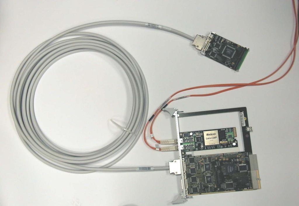
7 NIC Myrinet IN_1 Commercial card 64kB PCI connector 64-bit 66 or 100MHz JTAG connector IN_2 64kB FRL Function PCI 66 (528 MB/s) IN_3 64kB Memory 4Mbytes Bridge Compact PCI 32-bit 33MHz IN_4 64kB 64b@100MHz Compact PCI Back-plane -2 LVDS 400MB/s -64 Kbytes buffer for each link -Independent internal PCI bus (64b@66MHz) -A slot PCI for NIC card -4MB 64@100MHz to spy, histogram -One to internal logic ; one to interface with CPCI
8 NIC Myrinet IN_1 Commercial card 64kB PCI connector 64-bit 66 or 100MHz JTAG connector IN_2 64kB FRL Function PCI 66 (528 MB/s) 64kB Bridge IN_3 Memory 4Mbytes Compact PCI 32-bit 33MHz 64b@100MHz Compact PCI Back-plane 64kB IN_4-4 LVDS 400MB/s -64 Kbytes buffer for each link -Independent internal PCI bus (64b@66MHz) -A slot PCI for NIC card -4MB 64b@100MHz shared access to spy, histogram -One to internal logic ; one to interface with CPCI
9 FEATURES 1 to 4 Slink64 Input(s) Memory Flash to keep up to 4 designs -Normal functionality -Fragments generated inside FRL -.. Auto-check link IN_1 IN_2 IN_3 IN_4 64kB 64kB 64kB 64kB NIC PCI connector 64-bit Memory -Send events to NIC card memory blocks (with FRL header).each link can be disabled.one event fragment of each link are merged in one -Spies events (All events, on CRC error, on Evt#, out_of_sync..) -Histogram :.WC distribution of event size (256 points with programmable resolution).bunch crossing -Up to four designs uploaded inside the flash memory -The user can reprogram design to EEPROM and switch between designs remotely Spy fragments : -all fragments -list of up to 1024 fragments numbers -on CRC error.. WC histogram for each links (256 pitches of programmable step:8 to 1K bytes) Bunch crossing histogram
10 FED# Trigger# Packet# 0 Payload size Reserved Data Page size PCI A B C D E F G H I J K Memory Page Header A,B,C K FRL header Payload Myrinet trailer Myrinet header FRL (Internal ) Myrinet (NIC) -Protocol used is push-mode (write has less overhead) -NIC board has a memory divided in memory pages (FRL_Header + data) -FRL header indicate the memory pages structure for each event -Memory page size can be adapted to optimize the throughput of the optical link through switches

11 Average Event fragment size -Blocs size 4KB


12 LVDS 350 MHz over 10 meters cable 2.8 ns -Long test duration was done without problem -One problem was discovered and solved with our preserie installation
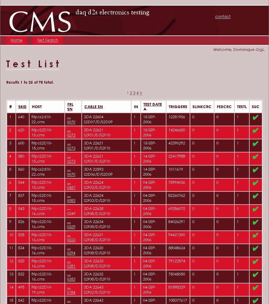
13 720 Slink cards and 560 FRL cards were produced last year. Four test benched were developed to validate the production and the installation before the commissioning. - Test bench 1 (card per card) : Electrical and board configuration (EEPROM, jumpers ) - Test bench 2 (4 cards at the time): using all functionalities, the test board was done (Component soldering, short-circuit, component dead.). - Test bench 3 (16 cards at the time with Myrinet board). The real functionality. - Test bench 4 (card per card) each card+cable was tested installed underground with a USB efed module. - All results are inserted in CMS database (see next slide) Card tested success FRL (100%) SLINK sender (99.7%) LVDS cable (99.8%) - All hardware is already installed at USC55 CMS. Test bench4 started


14 designs Test bench 1&2 Test bench 4
 CRC")
15 FRLversion Number of triggers FRL Serial number CMC version SLINK Status (backpressure, link down ) CRC error

16
17 Process (merges) the partition device states to form the detector partition status in a fast way (~100 ns) Monitors the dead time introduced by the partition devices Identification of (potential) pathologic FEDs Keeps a history memory of the state changes Allows to monitor the device states or playback for detailed analysis Generates input patterns for Trigger Control System Is also the output card for the atts
18 Compact PCI 6U double width form factor TTS connector allows standard RJ45 network cables At 40 MHz transition rate, LVDS drivers allows hundreds meter of cable length PCI control interface re-used from FRL design update Can be done remotly Through a JTAG connection

19 20 x RJ45 from lvds receivers JTAG connector FMM Function 32 MHz Private bus Bridge 2 X RJ45 to lvds drivers Memory 2Mbytes 64b@80MHz Compact PCI 32-bit 33MHz Compact PCI Back-plane Switches (Reset-reprog )
20 Standard RJ45 connector is used Low cost, reliable, small footprint, high-density front panel Socket with light-guides for bi-color LEDs Pin 1 -busy Pin 2 +busy Pin 3 -ready Pin 4 +overflow warning Pin 5 -overflow warning Pin 6 + ready Pin 7 -out of synch Pin 8 +out of synch
21 LV1A rate Fine Ready LV1A rate too high Warning Overflow LV1A rate reduced LV1A rate still too high LV1A rate reduced Busy Killing LV1A Out of sync Resynch Error Repair Reconnect Discon- nected
22 States are provided on 4 bits: max transition rate = 40 MHz but we expect ~100 Hz! 6 states defined for FEDs using 7 values 9 values reserved If a FED is in any reserved state, the FMM propagates a new state: illegal FEDs linked to an FMM can be in a different state: state priorities (decreasing order) are as follows: Disconnect Error Out_of_sync Busy Overflow Illegal Ready
23 24 connectors with LEDs, configurable as input or output at soldering time Allows to deal with 1 or 2 partitions and enable the card to be atts output Mask register a pathologic FED will not disturb the system once detected and identified Hardware dead-time monitors early detection of potential problem Cyclic history memory: only state transitions are recorded with time tag 2 MB/128 k transitions (16 bytes/transitions) Time tag resolution/range: 25 ns/40 bit (~7.6 hours) System clock at 80 MHz, Inputs sampled at 80 MHz but processed at 40 MHz History data can be pushed directly to host PC ( ala FEDKIT) (eeprom) can be reconfigured through PCI and JTAG connector
24 FMM tests : 2 stage test system Two FMM was mounted/configured as tester module (stts sequencer) :20 ports configured as output Test software with direct connection to database was developed. During the implementation of the test system a lot of firmware improvements have been added. 55 out of 60 (90%) modules where successfully tested. 5 need to be repaired (small problems). (46 are needed in CMS during operation)


25 -Production and tests are done -Production is installed -Slink cables installation is done, FMM cables installation is on going -Test on site has started
The Global Trigger Emulator System for the CMS experiment
 The Global Trigger Emulator System for the CMS experiment K. Zachariadou a1, T. Geralis 1, S. Kyriazopoulou 1, C. Markou 1, I. Michailakis 1 Abstract--We present the development of the Global Trigger Emulator
EMU FED. --- Crate and Electronics. ESR, CERN, November B. Bylsma, S. Durkin, Jason Gilmore, Jianhui Gu, T.Y. Ling. The Ohio State University
 EMU FED --- Crate and Electronics B. Bylsma, S. Durkin, Jason Gilmore, Jianhui Gu, T.Y. Ling The Ohio State University ESR, CERN, November 2004 EMU FED Design EMU FED: Outline FED Crate & Custom Backplane
2008 JINST 3 S Data Acquisition. Chapter 9
 Chapter 9 Data Acquisition The architecture of the CMS Data Acquisition (DAQ) system is shown schematically in figure 9.1. The CMS Trigger and DAQ system is designed to collect and analyse the detector
HCAL DCC Technical Reference E. Hazen - Revised March 27, 2007 Note: Latest version of this document should be available at:
 HCAL DCC Technical Reference E. Hazen - Revised March 27, 2007 Note: Latest version of this document should be available at: http://cmsdoc.cern.ch/cms/hcal/document/countinghouse/dcc/dcctechref.pdf Table
Global Trigger Processor Emulator
 Global Trigger Processor Emulator Dr. Katerina Zachariadou Athens University Paris Sphicas Vassilis Karageorgos (Diploma) NCSR Demokritos Theo Geralis Christos Markou Isidoros Michailakis (Electronics
10Gbps TCP/IP streams from the FPGA
 TWEPP 2013 10Gbps TCP/IP streams from the FPGA for the CMS DAQ Eventbuilder Network Petr Žejdl, Dominique Gigi on behalf of the CMS DAQ Group 26 September 2013 Outline CMS DAQ Readout System TCP/IP Introduction,
Read-out of High Speed S-LINK Data Via a Buffered PCI Card
 Read-out of High Speed S-LINK Data Via a Buffered PCI Card A. Guirao Talk for the 4 th PCaPAC International Workshop - This is the paper copy version of the presentation- Slide 9th is repeated due to an
RPC Trigger Overview
 RPC Trigger Overview presented by Maciek Kudla, Warsaw University RPC Trigger ESR Warsaw, July 8th, 2003 RPC Trigger Task The task of RPC Muon Trigger electronics is to deliver 4 highest momentum muons
Track-Finder Test Results and VME Backplane R&D. D.Acosta University of Florida
 Track-Finder Test Results and VME Backplane R&D D.Acosta University of Florida 1 Technical Design Report Trigger TDR is completed! A large amount effort went not only into the 630 pages, but into CSC Track-Finder
Alternative Ideas for the CALICE Back-End System
 Alternative Ideas for the CALICE Back-End System Matthew Warren and Gordon Crone University College London 5 February 2002 5 Feb 2002 Alternative Ideas for the CALICE Backend System 1 Concept Based on
Field Program mable Gate Arrays
 Field Program mable Gate Arrays M andakini Patil E H E P g r o u p D H E P T I F R SERC school NISER, Bhubaneshwar Nov 7-27 2017 Outline Digital electronics Short history of programmable logic devices
Readout-Nodes. Master-Node S-LINK. Crate Controller VME ROD. Read out data (PipelineBus) VME. PipelineBus Controller PPM VME. To DAQ (S-Link) PPM
 VME. PipelineBus Controller PPM VME. To DAQ (S-Link) PPM") THE READOUT BU OF THE ATLA LEVEL- CALORIMETER TRIGGER PRE-PROCEOR C. chumacher Institut fur Hochenergiephysik, Heidelberg, Germany (e-mail: schumacher@asic.uni-heidelberg.de) representing the ATLA level-
THE READOUT BU OF THE ATLA LEVEL- CALORIMETER TRIGGER PRE-PROCEOR C. chumacher Institut fur Hochenergiephysik, Heidelberg, Germany (e-mail: schumacher@asic.uni-heidelberg.de) representing the ATLA level-
The CMS Event Builder
 The CMS Event Builder Frans Meijers CERN/EP-CMD CMD on behalf of the CMS-DAQ group CHEP03, La Jolla, USA, March 24-28 28 2003 1. Introduction 2. Selected Results from the Technical Design Report R&D programme
Presentation Outline. Data Concentrator Card for ECAL. ECAL Data Volume and Raw Data generation. DCC Conceptual Design
 Data Concentrator Card for ECAL Presentation Outline ECAL Data Volume and Raw Data generation DCC Conceptual Design Modeling and Simulation of the Hardware DCC TEAM DCC Requirements João Varela ECAL Raw
ROB-IN Functional demonstrator of the ATLAS Trigger / DAQ Read-Out Buffer O.Gachelin, M.Huet, P.Le Dû, M.Mur C.E.A.
 1 ROB-IN Functional demonstrator of the ATLAS Trigger / DAQ Read-Out Buffer O.Gachelin, M.Huet, P.Le Dû, M.Mur C.E.A. Saclay - DAPNIA 2 Basic principles Data flow : output < input including L2 and L3 according
cpci-dart Base-Board & Daughter-Board
 DYNAMIC ENGINEERING 150 DuBois, Suite C Santa Cruz, CA 95060 (831) 457-8891 Fax (831) 457-4793 http://www.dyneng.com sales@dyneng.com Est. 1988 User Manual cpci-dart Base-Board & Daughter-Board Eight-Channel
SPECS : A SERIAL PROTOCOL FOR EXPERIMENT CONTROL SYSTEM IN LHCB.
 10th ICALEPCS Int. Conf. on Accelerator & Large Expt. Physics Control Systems. Geneva, 10-14 Oct 2005, WE1.5-4O (2005) : A SERIAL PROTOCOL FOR EXPERIMENT CONTROL SYSTEM IN LHCB. D.Breton, 1 D.Charlet,
TTC/TTS Tester (TTT) Module User Manual
 Module User Manual") TTC/TTS Tester (TTT) Module User Manual Eric Hazen hazen@bu.edu, Christopher Woodall cwoodall@bu.edu, Charlie Hill chill90@bu.edu May 24, 2013 1 Contents 1 Overview 3 2 Quick Start Guide 4 3 Hardware Description
TTC/TTS Tester (TTT) Module User Manual Eric Hazen hazen@bu.edu, Christopher Woodall cwoodall@bu.edu, Charlie Hill chill90@bu.edu May 24, 2013 1 Contents 1 Overview 3 2 Quick Start Guide 4 3 Hardware Description
AMC13 Register Display Documentation
 AMC13 Register Display Documentation Automatically Generated from status.cc in HCAL xdaq August 9, 2012 Status register at offset 0 in Virtex address space [ctrl regs] Reading this registers reports basic
BES-III off-detector readout electronics for the GEM detector: an update
 BES-III off-detector readout electronics for the GEM detector: an update The CGEM off-detector collaboration ( INFN/Univ. FE, INFN LNF, Univ. Uppsala ) 1 Outline Reminder Update on development status Off-detector
Using the FADC250 Module (V1C - 5/5/14)
") Using the FADC250 Module (V1C - 5/5/14) 1.1 Controlling the Module Communication with the module is by standard VME bus protocols. All registers and memory locations are defined to be 4-byte entities.
Using the FADC250 Module (V1C - 5/5/14) 1.1 Controlling the Module Communication with the module is by standard VME bus protocols. All registers and memory locations are defined to be 4-byte entities.
PCI to SH-3 AN Hitachi SH3 to PCI bus
 PCI to SH-3 AN Hitachi SH3 to PCI bus Version 1.0 Application Note FEATURES GENERAL DESCRIPTION Complete Application Note for designing a PCI adapter or embedded system based on the Hitachi SH-3 including:
PCI / PMC / CPCI / PCI-X Bus Analysis
 PCI / PMC / CPCI / PCI-X Bus Analysis Analyzer Exerciser Stimulus Target Anomaly Performance Compliance 850 System Analyzer/Exerciser Silicon Control Inc. introduces the ultimate analyzer and exerciser
Hera-B DAQ System and its self-healing abilities
 Hera-B DAQ System and its self-healing abilities V.Rybnikov, DESY, Hamburg 1. HERA-B experiment 2. DAQ architecture Read-out Self-healing tools Switch SLT nodes isolation 3. Run control system 4. Self-healing
IBM Network Processor, Development Environment and LHCb Software
 IBM Network Processor, Development Environment and LHCb Software LHCb Readout Unit Internal Review July 24 th 2001 Niko Neufeld, CERN 1 Outline IBM NP4GS3 Architecture A Readout Unit based on the NP4GS3
Readout Systems. Liquid Argon TPC Analog multiplexed ASICs SiPM arrays. CAEN 2016 / 2017 Product Catalog
 Readout Systems Liquid Argon TPC Analog multiplexed ASICs SiPM arrays CAEN 2016 / 2017 Product Catalog 192 Readout Systems SY2791 Liquid Argon TPC Readout System The SY2791 is a complete detector readout
Portable 2-Port Gigabit Wirespeed Streams Generator & Network TAP
 Portable 2-Port Gigabit Wirespeed Streams Generator & Network TAP NuDOG-301C OVERVIEW NuDOG-301C is a handheld device with two Gigabit ports for Ethernet testing. The main functions of NuDOG-301C include
Interconnection Structures. Patrick Happ Raul Queiroz Feitosa
 Interconnection Structures Patrick Happ Raul Queiroz Feitosa Objective To present key issues that affect interconnection design. Interconnection Structures 2 Outline Introduction Computer Busses Bus Types
Avnet, Xilinx ATCA PICMG Design Kit Hardware Manual
 user s guide Avnet, Xilinx ATCA PICMG Design Kit Hardware Manual Avnet Design Services 1 of 18 Rev 1.0 12/15/2004 Table of Contents 1 Overview... 5 2 Jumpers... 6 3 Personality Module Mechanicals... 8
CPCI-HPDI32ALT High-speed 64 Bit Parallel Digital I/O PCI Board 100 to 400 Mbytes/s Cable I/O with PCI-DMA engine
 CPCI-HPDI32ALT High-speed 64 Bit Parallel Digital I/O PCI Board 100 to 400 Mbytes/s Cable I/O with PCI-DMA engine Features Include: 200 Mbytes per second (max) input transfer rate via the front panel connector
Detector interface updates (SVD,ECL,EPID)
") Detector interface updates(svd,ecl,epid) M. Nakao p.1 Detector interface updates (SVD,ECL,EPID) Mikihiko Nakao(KEK-IPNS) mikihiko.nakao@kek.jp December 16, 2010 Belle II DAQ meeting, KEK Detector interface
Detector interface updates(svd,ecl,epid) M. Nakao p.1 Detector interface updates (SVD,ECL,EPID) Mikihiko Nakao(KEK-IPNS) mikihiko.nakao@kek.jp December 16, 2010 Belle II DAQ meeting, KEK Detector interface
ATLANTIS - a modular, hybrid FPGA/CPU processor for the ATLAS. University of Mannheim, B6, 26, Mannheim, Germany
 ATLANTIS - a modular, hybrid FPGA/CPU processor for the ATLAS Readout Systems A. Kugel, Ch. Hinkelbein, R. Manner, M. Muller, H. Singpiel University of Mannheim, B6, 26, 68131 Mannheim, Germany fkugel,
PC-MIP Link Receiver Board Interface Description
 PC-MIP Link Receiver Board Interface Description E. Hazen, A. Chertovskikh Boston University Rev 2. August 24, 26 1 Description and Operation This document describes briefly the PC-MIP 3-channel Link Receiver
ATLAS TDAQ RoI Builder and the Level 2 Supervisor system
 ATLAS TDAQ RoI Builder and the Level 2 Supervisor system R. E. Blair 1, J. Dawson 1, G. Drake 1, W. Haberichter 1, J. Schlereth 1, M. Abolins 2, Y. Ermoline 2, B. G. Pope 2 1 Argonne National Laboratory,
DEVBOARD3 DATASHEET. 10Mbits Ethernet & SD card Development Board PIC18F67J60 MICROCHIP
 DEVBOARD3 DATASHEET 10Mbits Ethernet & SD card PIC18F67J60 MICROCHIP Version 1.0 - March 2009 DEVBOARD3 Version 1.0 March 2009 Page 1 of 7 The DEVBOARD3 is a proto-typing board used to quickly and easily
2008 JINST 3 S Online System. Chapter System decomposition and architecture. 8.2 Data Acquisition System
 Chapter 8 Online System The task of the Online system is to ensure the transfer of data from the front-end electronics to permanent storage under known and controlled conditions. This includes not only
Ethernet Networks for the ATLAS Data Collection System: Emulation and Testing
 Ethernet Networks for the ATLAS Data Collection System: Emulation and Testing F. Barnes, R. Beuran, R. W. Dobinson, M. J. LeVine, Member, IEEE, B. Martin, J. Lokier, and C. Meirosu Abstract-- This paper
CMS Conference Report
 Available on CMS information server CMS CR 2007/016 FERMILAB-CONF-07-364-E CMS Conference Report 15 May 2007 CMS DAQ Event Builder Based on Gigabit Ethernet G. Bauer, V. Boyer, J. Branson, A. Brett, E.
10 Gbps TCP/IP streams from the FPGA for the CMS DAQ eventbuilder network
 Home Search Collections Journals About Contact us My IOPscience 10 Gbps TCP/IP streams from the FPGA for the CMS DAQ eventbuilder network This content has been downloaded from IOPscience. Please scroll
TI s PCI2040 PCI-to-DSP Bridge
 TI s PCI2040 PCI-to-DSP Bridge Brian G. Carlson - Sr. DSP Engineer DNA Enterprises, Inc. August 5, 1999 E-mail: bcarlson@dnaent.com 1 Agenda Introduction to the PCI Bus DSP Host Port Interface (HPI) Overview
Electronics on the detector Mechanical constraints: Fixing the module on the PM base.
 PID meeting Mechanical implementation ti Electronics architecture SNATS upgrade proposal Christophe Beigbeder PID meeting 1 Electronics is split in two parts : - one directly mounted on the PM base receiving
The MROD. The MDT Precision Chambers ROD. Adriaan König University of Nijmegen. 5 October nd ATLAS ROD Workshop 1
 The MROD The MDT Precision Chambers ROD Adriaan König University of Nijmegen 5 October 2000 2nd ATLAS ROD Workshop 1 Contents System Overview MROD-0 Prototype MROD-1 Prototype Performance Study FE Parameter
The FTK to Level-2 Interface Card (FLIC)
") The FTK to Level-2 Interface Card (FLIC) J. Anderson, B. Auerbach, R. Blair, G. Drake, A. Kreps, J. Love, J. Proudfoot, M. Oberling, R. Wang, J. Zhang November 5th, 2015 2015 IEEE Nuclear Science Symposium
The FTK to Level-2 Interface Card (FLIC) J. Anderson, B. Auerbach, R. Blair, G. Drake, A. Kreps, J. Love, J. Proudfoot, M. Oberling, R. Wang, J. Zhang November 5th, 2015 2015 IEEE Nuclear Science Symposium
A Fast Ethernet Tester Using FPGAs and Handel-C
 A Fast Ethernet Tester Using FPGAs and Handel-C R. Beuran, R.W. Dobinson, S. Haas, M.J. LeVine, J. Lokier, B. Martin, C. Meirosu Copyright 2000 OPNET Technologies, Inc. The Large Hadron Collider at CERN
TAG Word 0 Word 1 Word 2 Word 3 0x0A0 D2 55 C7 C8 0x0A0 FC FA AC C7 0x0A0 A5 A6 FF 00
 ELE 758 Final Examination 2000: Answers and solutions Number of hits = 15 Miss rate = 25 % Miss rate = [5 (misses) / 20 (total memory references)]* 100% = 25% Show the final content of cache using the
Trigger and Data Acquisition at the Large Hadron Collider
 Trigger and Data Acquisition at the Large Hadron Collider Acknowledgments (again) This overview talk would not exist without the help of many colleagues and all the material available online I wish to
CPCI-SIP. Slave Dual IndustryPack Carrier for 3U CompactPCI systems REFERENCE MANUAL Version 2.0 June 1998
 CPCI-SIP Slave Dual IndustryPack Carrier for 3U CompactPCI systems REFERENCE MANUAL 729-20-000-4000 Version 2.0 June 1998 ALPHI TECHNOLOGY CORPORATION 6202 S. Maple Avenue #120 Tempe, AZ 85283 USA Tel:
RHiNET-3/SW: an 80-Gbit/s high-speed network switch for distributed parallel computing
 RHiNET-3/SW: an 0-Gbit/s high-speed network switch for distributed parallel computing S. Nishimura 1, T. Kudoh 2, H. Nishi 2, J. Yamamoto 2, R. Ueno 3, K. Harasawa 4, S. Fukuda 4, Y. Shikichi 4, S. Akutsu
Centre de Physique des Particules de Marseille. The PCIe-based readout system for the LHCb experiment
 The PCIe-based readout system for the LHCb experiment K.Arnaud, J.P. Duval, J.P. Cachemiche, Cachemiche,P.-Y. F. Réthoré F. Hachon, M. Jevaud, R. Le Gac, Rethore Centre de Physique des Particules def.marseille
The ASDEX Upgrade UTDC and DIO cards - A family of PCI/cPCI devices for Real-Time DAQ under Solaris
 The ASDEX Upgrade UTDC and DIO cards - A family of PCI/cPCI devices for Real-Time DAQ under Solaris A. Lohs a, K. Behler a,*, G. Raupp, Unlimited Computer Systems b, ASDEX Upgrade Team a a Max-Planck-Institut
Scintillator-strip Plane Electronics
 Scintillator-strip Plane Electronics Mani Tripathi Britt Holbrook (Engineer) Juan Lizarazo (Grad student) Peter Marleau (Grad student) Tiffany Landry (Junior Specialist) Cherie Williams (Undergrad student)
Technical Information Manual
 Technical Information Manual Revision n. 3 28 August 2002 MOD. V550 / V550 B MOD. V550 A / V550 AB 2 CHANNEL C-RAMS CAEN will repair or replace any product within the guarantee period if the Guarantor
Copyright DapTechnology B.V., All Rights Reserved
 DocRev 1.5, JAN2006 Copyright DapTechnology B.V., 1998-2006 - All Rights Reserved FireSpy 850/450b The FireSpy850 and FireSpy450b bus analyzers complete the second generation of FireWire analyzers offered
Vertex Detector Electronics: ODE to ECS Interface
 Vertex Detector Electronics: ODE to ECS Interface LHCb Technical Note Issue: 1 Revision: 0 Reference: LHCb 2000-012 VELO Created: 1 February 2000 Last modified: 20 March 2000 Prepared By: Yuri Ermoline
USBIO24 RL Digital I/O Module
 Ether I/O 24 Digital I/O Module The Ether I/O 24 is an UDP/IP controlled digital Input/Output module. The module features three 8-bit ports with 5V level signal lines. Each of the 24 lines can be independently
XC164CS Prototype Board
 XC164CS Prototype Board Features: Small PCB (95 x 57 mm) with ground plane. o Designed to fit inside a Pac Tec FLX-4624 ABS enclosure Infineon XC164CS 16-bit single-chip microcontroller o 166SV2 core o
ROBIN Functional demonstrator of the ATLAS Trigger / DAQ Read-Out Buffer O.Gachelin, M.Huet, P.Le Dû, M.Mur C.E.A. Saclay - DAPNIA
 1 ROBIN Functional demonstrator of the ATLAS Trigger / DAQ Read-Out Buffer O.Gachelin, M.Huet, P.Le Dû, M.Mur C.E.A. Saclay - DAPNIA 2 Basic principles Data flow : output < input including L2 and L3 according
XMC4800 EtherCAT APP SSC Firmware Update Slave Example. Getting Started Version 3.0
 XMC4800 EtherCAT APP SSC Firmware Update Slave Example Getting Started Version 3.0 1 2 3 4 5 6 7 Overview and requirements Setup Short overview boot modes Architecture Implementation of the application
ACTL-TIME: Report on recent activities. Arnim Balzer for the ACTL-TIME sub-work package ACTL-TIME Camera Call, SeeVogh July 1, 2016
 ACTL-TIME: Report on recent activities Arnim Balzer for the ACTL-TIME sub-work package ACTL-TIME Camera Call, SeeVogh July 1, 2016 Reminder: Mailing Lists Created two temporary mailing lists until official
Wave Generator Xpress
 ! READ THIS FIRST! This revision of Wave Generator Data Sheet is valid for devices sold from September 2011. Please check your unit hardware revision. The hardware revision is composed of the 2 first digits
eip-10 Embedded TCP/IP 10-BaseT Network Module Features Description Applications
 Embedded TCP/IP 10-BaseT Network Module Features 8-bit reprogrammable Microcontroller with Enhanced Flash program memory, EEPROM and Static RAM data memory On board 10Mbps Ethernet controller, and RJ45
RTE-V850E/GP1-IE USER'S MANUAL (REV.1.01) RealTimeEvaluator
 RealTimeEvaluator") RTE-V850E/GP1-IE USER'S MANUAL (REV.1.01) RealTimeEvaluator REVISION HISTORY Rev. 1.00 June 20, 2002 Rev. 1.01 November 15, 2002 First edition Revising following chapters * "Measured value of execution
RTE-V850E/GP1-IE USER'S MANUAL (REV.1.01) RealTimeEvaluator REVISION HISTORY Rev. 1.00 June 20, 2002 Rev. 1.01 November 15, 2002 First edition Revising following chapters * "Measured value of execution
Embedded Development Platform
 Embedded Development Platform Getting Started Guide for the ARM mbed Carrier Module EDP-CM-mbed Version 3.11 February 2011 Contents 1. Introduction 3 2. Prepare to run the Hello World Program 4 2.1 Software
ROB IN Performance Measurements
 ROB IN Performance Measurements I. Mandjavidze CEA Saclay, 91191 Gif-sur-Yvette CEDEX, France ROB Complex Hardware Organisation Mode of Operation ROB Complex Software Organisation Performance Measurements
S-LINK: A Prototype of the ATLAS Read-out Link
 : A Prototype of the ATLAS Read-out Link Erik van der Bij, Robert McLaren, Zoltán Meggyesi EP-Division CERN, CH-1211 Geneva 23 Abstract The ATLAS data acquisition system needs over 1500 read-out links
Artisan Technology Group is your source for quality new and certified-used/pre-owned equipment
 Artisan Technology Group is your source for quality new and certified-used/pre-owned equipment FAST SHIPPING AND DELIVERY TENS OF THOUSANDS OF IN-STOCK ITEMS EQUIPMENT DEMOS HUNDREDS OF MANUFACTURERS SUPPORTED
USCMS HCAL FERU: Front End Readout Unit. Drew Baden University of Maryland February 2000
 USCMS HCAL FERU: Front End Readout Unit Drew Baden University of Maryland February 2000 HCAL Front-End Readout Unit Joint effort between: University of Maryland Drew Baden (Level 3 Manager) Boston University
Chapter 11: Input/Output Organisation. Lesson 15: Standard I/O bus PCI
 Chapter 11: Input/Output Organisation Lesson 15: Standard I/O bus PCI Objective Familiar with I/O bus and standard I/O interfaces parallel bus PCI (Peripheral Connect Interface) for a synchronous parallel
Programming in the MAXQ environment
 AVAILABLE The in-circuit debugging and program-loading features of the MAXQ2000 microcontroller combine with IAR s Embedded Workbench development environment to provide C or assembly-level application
Machine Vision Camera Interfaces. Korean Vision Show April 2012
 Machine Vision Camera Interfaces Korean Vision Show April 2012 Vision Interfaces Page 1 Machine Vision Hardware Interface Standards PCI, CPCI V2.2, PCIe V2.x USB2, USB3 Vision IEEE1394 (no development
Description of the JRA1 Trigger Logic Unit (TLU), v0.2c
, v0.2c") EUDET Description of the JRA1 Trigger Logic Unit (TLU), v0.2c D. Cussans September 11, 2009 Abstract This document is an updated version of EUDET-Memo-2008-50. It describes the interfaces and operation
EUDET Description of the JRA1 Trigger Logic Unit (TLU), v0.2c D. Cussans September 11, 2009 Abstract This document is an updated version of EUDET-Memo-2008-50. It describes the interfaces and operation
EM100Pro Serial Flash Emulator Specification
 EM100Pro Serial Flash Emulator Specification V1.5 Simply the best solution to develop code on SPI Flash memories Emulate all the market Serial Flash Designed to support the future Serial Flash evolution:
Computer buses and interfaces
 FYS3240-4240 Data acquisition & control Computer buses and interfaces Spring 2018 Lecture #7 Reading: RWI Ch7 and page 559 Bekkeng 14.02.2018 Abbreviations B = byte b = bit M = mega G = giga = 10 9 k =
Intelop. *As new IP blocks become available, please contact the factory for the latest updated info.
 A FPGA based development platform as part of an EDK is available to target intelop provided IPs or other standard IPs. The platform with Virtex-4 FX12 Evaluation Kit provides a complete hardware environment
FT245 USB Modual. - Ver FT245 Module Features
 1. FT245 Module Features FT245 USB Modual - Ver 1.0 - - FTDI chip 사의 FT245 채용 - D2XX Driver 사용시최대 1MByte 전송 - 1 열 Pin Header 에 Data, Control Pin 입출력 - 외부 I/O 전원선택가능 (3.3V, 5V) - USB 정보저장을위한 EEPROM Socket
Data Link Control Protocols
 Protocols : Introduction to Data Communications Sirindhorn International Institute of Technology Thammasat University Prepared by Steven Gordon on 23 May 2012 Y12S1L07, Steve/Courses/2012/s1/its323/lectures/datalink.tex,
PCI-X Bus PCI Express Bus Variants for Portable Computers Variants for Industrial Systems
 PCI Bus Variants PCI-X Bus PCI Express Bus Variants for Portable Computers Variants for Industrial Systems 1 Variants for Portable Computers Mini PCI PCMCIA Standards CardBus ExpressCard 2 Specifications
FEC. Front End Control unit for Embedded Slow Control D R A F T. C. Ljuslin C. Paillard
 FEC Front End Control unit for Embedded Slow Control C. Ljuslin C. Paillard D R A F T A. M. FECSpecs.doc DRAFT - 0.84 1 7/22/2003 1. DOCUMENT HISTORY 000322 TIMEOUT in status reg 1added 000330 TTCRX_READY
XE 900: Fastest EPIC board now available with Windows XPe
 XE 900: Fastest EPIC board now available with Windows XPe The XE 900 SBC is a high performance, low power, x86 workhorse for embedded applications. It is an EPIC form factor SBC with a rich family of I/O
TOF Electronics. J. Schambach University of Texas Review, BNL, 2 Aug 2007
 TOF Electronics J. Schambach University of Texas Review, BNL, 2 Aug 2007 1 Outline Electronics Overview Trigger & DAQ Interfaces Board Status, Tests & Plans 2 Electronics for One Side 3 Tray Level Electronics
S2C K7 Prodigy Logic Module Series
 S2C K7 Prodigy Logic Module Series Low-Cost Fifth Generation Rapid FPGA-based Prototyping Hardware The S2C K7 Prodigy Logic Module is equipped with one Xilinx Kintex-7 XC7K410T or XC7K325T FPGA device
SMT229. Ethernet TRAM User's Guide
 Preliminary SMT229 Ethernet TRAM User's Guide Overview... 2 Intended audience... 2 Description... 2 Physical... 2 Ethernet installation... 3 GSL sub-miniature transceiver... 3 Third party transceiver/dc-dc
Schematic. A: Overview of the Integrated Detector Readout Electronics and DAQ-System. optical Gbit link. 1GB DDR Ram.
 A: Overview of the Integrated Detector Readout Electronics and DAQ-System N s CASCADE Detector Frontend (X0) (X) (Y0) (Y) optional: CIPix- Board (T) Optical Gigabit Link CDR.0 FPGA based readout board
ARINC-629 Interface to PMC Sy629PMC-BPM
 ARINC-629 Interface to PMC Sy629PMC-BPM Summary features Interface compatible with 32bit PCI Local bus Specification, revision 2.1, June 1995 PCI interrupts on Module Events Single width PMC Module Uses
ATM-DB Firmware Specification E. Hazen Updated January 4, 2007
 ATM-DB Firmware Specification E. Hazen Updated January 4, 2007 This document describes the firmware operation of the Ethernet Daughterboard for the ATM for Super- K (ATM-DB). The daughterboard is controlled
5I24 ANYTHING I/O MANUAL
 5I24 ANYTHING I/O MANUAL Version 1.5 This page intentionally not blank Table of Contents GENERAL.......................................................... 1 DESCRIPTION.................................................
Introduction. SDIO Bus
 In this Application Note we discuss the SDIO Protocol, the challenges involved in Protocol breakdown and PGY-SSM comprehensive Protocol Analysis solution for decode and analysis. Introduction. SDIO offers
Prototyping NGC. First Light. PICNIC Array Image of ESO Messenger Front Page
 Prototyping NGC First Light PICNIC Array Image of ESO Messenger Front Page Introduction and Key Points Constructed is a modular system with : A Back-End as 64 Bit PCI Master/Slave Interface A basic Front-end
EASY-NIM 928 Suite. High Performance, Multi-Function Nuclear MCA/Counter/Timer/Rate Meter
 High Performance, Multi-Function Nuclear MCA/Counter/Timer/Rate Meter A unique, PC-enabled NIM solution delivering unmatched flexibility, reliability, and ease-of-use. Introduction The ORTEC EASY-NIM 928
ARDUINO MINI 05 Code: A000087
 ARDUINO MINI 05 Code: A000087 The Arduino Mini is a very compact version of the Arduino Nano without an on board USB to Serial connection The Arduino Mini 05 is a small microcontroller board originally
Design of a Gigabit Distributed Data Multiplexer and Recorder System
 Design of a Gigabit Distributed Data Multiplexer and Recorder System Abstract Albert Berdugo VP of Advanced Product Development Teletronics Technology Corporation Bristol, PA Historically, instrumentation
Product type designation. General information. Supply voltage. Input current
 Data sheet SIMATIC S7-300, CPU 312C COMPACT CPU WITH MPI, 10 DI/6 DO, 2 FAST COUNTERS (10 KHZ), INTEGRATED 24V DC POWER SUPPLY, 64 KBYTE WORKING MEMORY, FRONT CONNECTOR (1 X 40PIN) AND MICRO MEMORY CARD
Token Bit Manager for the CMS Pixel Readout
 Token Bit Manager for the CMS Pixel Readout Edward Bartz Rutgers University Pixel 2002 International Workshop September 9, 2002 slide 1 TBM Overview Orchestrate the Readout of Several Pixel Chips on a
Computer Architecture CS 355 Busses & I/O System
 Computer Architecture CS 355 Busses & I/O System Text: Computer Organization & Design, Patterson & Hennessy Chapter 6.5-6.6 Objectives: During this class the student shall learn to: Describe the two basic
Separate 24-bit Read/Write Busses Simple FNAD commanding: e.g. F = 0 (read) N = 1 (crate slot) A = card channel # D = data (either)
 N = 1 (crate slot) A = card channel # D = data (either)") NIM Standard NIM is an acronym for Nuclear Instrumentation Methods. The NIM standard (DOE/ER-0457) was established in 1964 for the nuclear and high energy physics communities. The goal of NIM was to promote
NIM Standard NIM is an acronym for Nuclear Instrumentation Methods. The NIM standard (DOE/ER-0457) was established in 1964 for the nuclear and high energy physics communities. The goal of NIM was to promote
CHAPTER 3 WIRELESS MEASUREMENT INSTRUMENT
 CHAPTER 3 WIRELESS MEASUREMET ISTRUMET This chapter gives a functional description of the WMI hardware and software for implementation in IVDS. A detailed technical description is not given, but is provided
BTeV at C0. p p. Tevatron CDF. BTeV - a hadron collider B-physics experiment. Fermi National Accelerator Laboratory. Michael Wang
 BTeV Trigger BEAUTY 2003 9 th International Conference on B-Physics at Hadron Machines Oct. 14-18, 2003, Carnegie Mellon University, Fermilab (for the BTeV collaboration) Fermi National Accelerator Laboratory
Ignacy Kudla, Radomir Kupczak, Krzysztof Pozniak, Antonio Ranieri
 *** Draft *** 15/04/97 *** MK/RK/KTP/AR *** ***use color print!!!*** RPC Muon Trigger Detector Control Ignacy Kudla, Radomir Kupczak, Krzysztof Pozniak, Antonio Ranieri $Ã&06 Ã*(1(5$/ RPC Muon Trigger
CMX Hardware Status. Chip Brock, Dan Edmunds, Philippe Yuri Ermoline, Duc Bao Wojciech UBC
 Hardware Status Chip Brock, Dan Edmunds, Philippe Laurens@MSU Yuri Ermoline, Duc Bao Ta @CERN Wojciech Fedorko @ UBC Michigan State University 25-Oct-2013 Outline Review of hardware project (Some) hardware
User's Manual. PXI Power Distribution Module
 User's Manual PXI Power Distribution Module Version 2.5, June 2010 XIA LLC 31057 Genstar Road Hayward, CA 94544 USA Phone: (510) 401-5760; Fax: (510) 401-5761 http://www.xia.com Disclaimer Information