Advanced FPGA Design Methodologies with Xilinx Vivado
|
|
|
- Damian Tate
- 5 years ago
- Views:
Transcription
1 Advanced FPGA Design Methodologies with Xilinx Vivado Lecturer: Alexander Jäger Course of studies: Technische Informatik Student number: Date: /01/15 Advanced FPGA Design Methodologies with Xilinx Vivado
2 Advanced FPGA Design Methodologies with Xilinx Vivado - What are FPGAs - Fields of applications - Basic FPGA Design Flow - Vivado Standard Design Flow - Incremental Compile - Test Setup & Results - Conclusion 2
3 What are FPGAs The field-programmable gate array (FPGA) is a semiconductor device that can be programmed after manufacturing. Instead of being restricted to any predetermined hardware function, an FPGA allows you to program product features and functions [...]. You can use an FPGA to implement any logical function... Altera Corporation - FPGAs, , 19:21 3
4 What are FPGAs Structure: National Instruments Corporation - Wie funktionieren FPGAs? , 19:33 4
5 What are FPGAs Structure of a logic block: Xilinx Inc. - Spartan-3E FPGA Family Data Sheet, ,P.23 5
6 What are FPGAs Structure of a SLICE: Xilinx Inc. - Spartan-3E FPGA Family Data Sheet, ,P.23 6
7 Advanced FPGA Design Methodologies with Xilinx Vivado - What are FPGAs - Fields of applications - Basic FPGA Design Flow - Vivado Standard Design Flow - Incremental Compile - Test Setup & Results - Conclusion 7
8 Fields of applications - Digital systems with small to medium quantities - Prototyping of digital systems for evaluation and verification 8
9 Fields of applications Reasons: All possible digital functions can be implemented User programmable Easy changes of the Implementation No mask costs 9
10 Fields of applications Disadvantages: No (flexible) analogue elements FPGA is slower and needs more power than an ASIC with same function Price per chip in High Volume Production relatively high 10
11 Advanced FPGA Design Methodologies with Xilinx Vivado - What are FPGAs - Fields of applications - Basic FPGA Design Flow - Vivado Standard Design Flow - Incremental Compile - Test Setup & Results - Conclusion 11

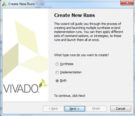
12 Basic FPGA Design Flow 12
13 Basic FPGA Design Flow Functional Specification Minimal Example: Implement a Fibonacci number generator Inputs: Reset (positive), Enable, Clock Outputs: 16-Bit Fibonacci Number Target Frequency: 300 Mhz Frequency of sampling device: 200 Mhz IO-Standard: LVCMOS25 13
14 Basic FPGA Design Flow 14
15 Basic FPGA Design Flow 15
16 Basic FPGA Design Flow 16
17 Basic FPGA Design Flow 17

18 Basic FPGA Design Flow 18

19 Basic FPGA Design Flow 19

20 Basic FPGA Design Flow 20

21 Basic FPGA Design Flow 21

22 Basic FPGA Design Flow 22
23 Advanced FPGA Design Methodologies with Xilinx Vivado - What are FPGAs - Fields of applications - Basic FPGA Design Flow - Vivado Standard Design Flow - Incremental Compile - Test Setup & Results - Conclusion 23
24 Vivado Standard Design Flow Xilinx Inc. - Vivado Design SuiteUser Guide Design Flows Overview, , P.6 24

25 Vivado Standard Design Flow 25
26 Advanced FPGA Design Methodologies with Xilinx Vivado - What are FPGAs - Fields of applications - Basic FPGA Design Flow - Vivado Standard Design Flow - Incremental Compile - Test Setup & Results - Conclusion 26

27 Incremental Compile Xilinx Inc. - Vivado Design Suite User Guide Implementation P.83 27

28 Incremental Compile 28

29 Incremental Compile 29
30 Incremental Compile Short Summary: A minimum of 85% match between original and new netlist required Design Checkpoint from previous Implementation needed Checkpoint can be (partially) placed or (partially) placed and (partially) routed 30
31 Advanced FPGA Design Methodologies - What are FPGAs - Fields of applications with Xilinx Vivado - Basic FPGA Design Flow - Vivado Standard Design Flow - Incremental Compile - Test Setup & Results - Conclusion 31
32 Test Setup & Results Starting Point: Fully implemented design with checkpoints List of small to big changes 2 runs for every list entry One with Standard Flow, One with Incremental Compile Compare: Runtime, Timing, Resource Utilization 32
33 Test Setup & Results 33

34 Test Setup & Results 34
35 Test Setup & Results Runtime Facts: Best measured runtime reduction: % Best theoretical reduction: % Average runtime reduction: 6.19 % Additional runtime inducted trough Incremental Compile: 1:45 min 35
36 Test Setup & Results Timing results: No influence, all required timings met 36
37 Test Setup & Results Resource utilization: No influence on used Block Ram and Slice Registers Utilization of Slice LUTs, LUT FF-Pairs and used Slices stayed same or dropped a bit 37
38 Advanced FPGA Design Methodologies - What are FPGAs - Fields of applications with Xilinx Vivado - Basic FPGA Design Flow - Vivado Standard Design Flow - Incremental Compile - Test Setup & Results - Conclusion 38
39 Conclusion Incremental Compile: Easy to use Overall small runtime reductions Sometimes small resource utilization reductions => Only minor improvements, still recommended for usage 39

40 Discussion Any Questions? Xilinx IC: 40
Advanced FPGA Design Methodologies with Xilinx Vivado
 Advanced FPGA Design Methodologies with Xilinx Vivado Alexander Jäger Computer Architecture Group Heidelberg University, Germany Abstract With shrinking feature sizes in the ASIC manufacturing technology,
Chapter 5: ASICs Vs. PLDs
 Chapter 5: ASICs Vs. PLDs 5.1 Introduction A general definition of the term Application Specific Integrated Circuit (ASIC) is virtually every type of chip that is designed to perform a dedicated task.
Digital Integrated Circuits
 Digital Integrated Circuits Lecture 9 Jaeyong Chung Robust Systems Laboratory Incheon National University DIGITAL DESIGN FLOW Chung EPC6055 2 FPGA vs. ASIC FPGA (A programmable Logic Device) Faster time-to-market
EECS150 - Digital Design Lecture 6 - Field Programmable Gate Arrays (FPGAs)
") EECS150 - Digital Design Lecture 6 - Field Programmable Gate Arrays (FPGAs) September 12, 2002 John Wawrzynek Fall 2002 EECS150 - Lec06-FPGA Page 1 Outline What are FPGAs? Why use FPGAs (a short history
EECS150 - Digital Design Lecture 6 - Field Programmable Gate Arrays (FPGAs) September 12, 2002 John Wawrzynek Fall 2002 EECS150 - Lec06-FPGA Page 1 Outline What are FPGAs? Why use FPGAs (a short history
Outline. EECS150 - Digital Design Lecture 6 - Field Programmable Gate Arrays (FPGAs) FPGA Overview. Why FPGAs?
 FPGA Overview. Why FPGAs?") EECS150 - Digital Design Lecture 6 - Field Programmable Gate Arrays (FPGAs) September 12, 2002 John Wawrzynek Outline What are FPGAs? Why use FPGAs (a short history lesson). FPGA variations Internal logic
EECS150 - Digital Design Lecture 6 - Field Programmable Gate Arrays (FPGAs) September 12, 2002 John Wawrzynek Outline What are FPGAs? Why use FPGAs (a short history lesson). FPGA variations Internal logic
INTRODUCTION TO FPGA ARCHITECTURE
 3/3/25 INTRODUCTION TO FPGA ARCHITECTURE DIGITAL LOGIC DESIGN (BASIC TECHNIQUES) a b a y 2input Black Box y b Functional Schematic a b y a b y a b y 2 Truth Table (AND) Truth Table (OR) Truth Table (XOR)
FPGA Based Digital Design Using Verilog HDL
 FPGA Based Digital Design Using Course Designed by: IRFAN FAISAL MIR ( Verilog / FPGA Designer ) irfanfaisalmir@yahoo.com * Organized by Electronics Division Integrated Circuits Uses for digital IC technology
Field Programmable Gate Array (FPGA)
") Field Programmable Gate Array (FPGA) Lecturer: Krébesz, Tamas 1 FPGA in general Reprogrammable Si chip Invented in 1985 by Ross Freeman (Xilinx inc.) Combines the advantages of ASIC and uc-based systems
Field Programmable Gate Array (FPGA) Lecturer: Krébesz, Tamas 1 FPGA in general Reprogrammable Si chip Invented in 1985 by Ross Freeman (Xilinx inc.) Combines the advantages of ASIC and uc-based systems
PINE TRAINING ACADEMY
 PINE TRAINING ACADEMY Course Module A d d r e s s D - 5 5 7, G o v i n d p u r a m, G h a z i a b a d, U. P., 2 0 1 0 1 3, I n d i a Digital Logic System Design using Gates/Verilog or VHDL and Implementation
10GBase-R PCS/PMA Controller Core
 10GBase-R PCS/PMA Controller Core Contents 1 10GBASE-R PCS/PMA DATA SHEET 1 1.1 FEATURES.................................................. 1 1.2 APPLICATIONS................................................
EITF35: Introduction to Structured VLSI Design
 EITF35: Introduction to Structured VLSI Design Introduction to FPGA design Rakesh Gangarajaiah Rakesh.gangarajaiah@eit.lth.se Slides from Chenxin Zhang and Steffan Malkowsky WWW.FPGA What is FPGA? Field
SHA3 Core Specification. Author: Homer Hsing
 SHA3 Core Specification Author: Homer Hsing homer.hsing@gmail.com Rev. 0.1 January 29, 2013 This page has been intentionally left blank. www.opencores.org Rev 0.1 ii Rev. Date Author Description 0.1 01/29/2013
Design Once with Design Compiler FPGA
 Design Once with Design Compiler FPGA The Best Solution for ASIC Prototyping Synopsys Inc. Agenda Prototyping Challenges Design Compiler FPGA Overview Flexibility in Design Using DC FPGA and Altera Devices
FPGAs in a Nutshell - Introduction to Embedded Systems-
 FPGAs in a Nutshell - Introduction to Embedded Systems- Dipl.- Ing. Falk Salewski Lehrstuhl Informatik RWTH Aachen salewski@informatik.rwth-aachen.de Winter term 6/7 Contents History FPGA architecture
Utility Reduced Logic (v1.00a)
") DS482 December 2, 2009 Introduction The Utility Reduced Logic core applies a logic reduction function over an input vector to generate a single bit result. The core is intended as glue logic between peripherals.
DS482 December 2, 2009 Introduction The Utility Reduced Logic core applies a logic reduction function over an input vector to generate a single bit result. The core is intended as glue logic between peripherals.
FPGA How do they work?
 ent FPGA How do they work? ETI135, Advanced Digital IC Design What is a FPGA? Manufacturers Distributed RAM History FPGA vs ASIC FPGA and Microprocessors Alternatives to FPGAs Anders Skoog, Stefan Granlund
FPGA system development What you need to think about. Frédéric Leens, CEO
 FPGA system development What you need to think about Frédéric Leens, CEO About Byte Paradigm 2005 : Founded by 3 ASIC-SoC-FPGA engineers as a Design Center for high-end FPGA and board design. 2007 : GP
Early Models in Silicon with SystemC synthesis
 Early Models in Silicon with SystemC synthesis Agility Compiler summary C-based design & synthesis for SystemC Pure, standard compliant SystemC/ C++ Most widely used C-synthesis technology Structural SystemC
Digital System Design Lecture 7: Altera FPGAs. Amir Masoud Gharehbaghi
 Digital System Design Lecture 7: Altera FPGAs Amir Masoud Gharehbaghi amgh@mehr.sharif.edu Table of Contents Altera FPGAs FLEX 8000 FLEX 10k APEX 20k Sharif University of Technology 2 FLEX 8000 Block Diagram
Design Methodologies. Full-Custom Design
 Design Methodologies Design styles Full-custom design Standard-cell design Programmable logic Gate arrays and field-programmable gate arrays (FPGAs) Sea of gates System-on-a-chip (embedded cores) Design
Design Methodologies and Tools. Full-Custom Design
 Design Methodologies and Tools Design styles Full-custom design Standard-cell design Programmable logic Gate arrays and field-programmable gate arrays (FPGAs) Sea of gates System-on-a-chip (embedded cores)
System Verification of Hardware Optimization Based on Edge Detection
 Circuits and Systems, 2013, 4, 293-298 http://dx.doi.org/10.4236/cs.2013.43040 Published Online July 2013 (http://www.scirp.org/journal/cs) System Verification of Hardware Optimization Based on Edge Detection
Graduate Institute of Electronics Engineering, NTU FPGA Design with Xilinx ISE
 FPGA Design with Xilinx ISE Presenter: Shu-yen Lin Advisor: Prof. An-Yeu Wu 2005/6/6 ACCESS IC LAB Outline Concepts of Xilinx FPGA Xilinx FPGA Architecture Introduction to ISE Code Generator Constraints
Digital Blocks Semiconductor IP
 Digital Blocks Semiconductor IP TFT Controller General Description The Digital Blocks TFT Controller IP Core interfaces a microprocessor and frame buffer memory via the AMBA 2.0 to a TFT panel. In an FPGA,
Scrypt ASIC Prototyping Preliminary Design Document
 Scrypt ASIC Prototyping Preliminary Design Document 1/13 Revision History Version Date Author Remarks Approved by v0.1 2/13 Contents 1 Scrypt Algorithm... 5 2 Major blocks in a Scrypt core... 6 3 Internal
Spiral 2-8. Cell Layout
 2-8.1 Spiral 2-8 Cell Layout 2-8.2 Learning Outcomes I understand how a digital circuit is composed of layers of materials forming transistors and wires I understand how each layer is expressed as geometric
! Program logic functions, interconnect using SRAM. ! Advantages: ! Re-programmable; ! dynamically reconfigurable; ! uses standard processes.
 Topics! SRAM-based FPGA fabrics:! Xilinx.! Altera. SRAM-based FPGAs! Program logic functions, using SRAM.! Advantages:! Re-programmable;! dynamically reconfigurable;! uses standard processes.! isadvantages:!
ECE 3220 Digital Design with VHDL. Course Information. Lecture 1
 ECE 3220 Digital Design with VHDL Course Information Lecture 1 Course Information Course #: ECE 3220 Course Name: Digital Design with VHDL Course Instructor: Dr. Vida Vakilian Email: vvakilian@csub.edu
Topics. Midterm Finish Chapter 7
 Lecture 9 Topics Midterm Finish Chapter 7 Xilinx FPGAs Chapter 7 Spartan 3E Architecture Source: Spartan-3E FPGA Family Datasheet CLB Configurable Logic Blocks Each CLB contains four slices Each slice
Simplify System Complexity
 1 2 Simplify System Complexity With the new high-performance CompactRIO controller Arun Veeramani Senior Program Manager National Instruments NI CompactRIO The Worlds Only Software Designed Controller
FPGA for Complex System Implementation. National Chiao Tung University Chun-Jen Tsai 04/14/2011
 FPGA for Complex System Implementation National Chiao Tung University Chun-Jen Tsai 04/14/2011 About FPGA FPGA was invented by Ross Freeman in 1989 SRAM-based FPGA properties Standard parts Allowing multi-level
L2: FPGA HARDWARE : ADVANCED DIGITAL DESIGN PROJECT FALL 2015 BRANDON LUCIA
 L2: FPGA HARDWARE 18-545: ADVANCED DIGITAL DESIGN PROJECT FALL 2015 BRANDON LUCIA 18-545: FALL 2014 2 Admin stuff Project Proposals happen on Monday Be prepared to give an in-class presentation Lab 1 is
Fast evaluation of nonlinear functions using FPGAs
 Adv. Radio Sci., 6, 233 237, 2008 Author(s) 2008. This work is distributed under the Creative Commons Attribution 3.0 License. Advances in Radio Science Fast evaluation of nonlinear functions using FPGAs
Introduction to Field Programmable Gate Arrays
 Introduction to Field Programmable Gate Arrays Lecture 1/3 CERN Accelerator School on Digital Signal Processing Sigtuna, Sweden, 31 May 9 June 2007 Javier Serrano, CERN AB-CO-HT Outline Historical introduction.
The Lekha 3GPP LTE FEC IP Core meets 3GPP LTE specification 3GPP TS V Release 10[1].
![The Lekha 3GPP LTE FEC IP Core meets 3GPP LTE specification 3GPP TS V Release 10[1].](/thumbs/75/72771698.jpg "The Lekha 3GPP LTE FEC IP Core meets 3GPP LTE specification 3GPP TS V Release 10[1].") Lekha IP 3GPP LTE FEC Encoder IP Core V1.0 The Lekha 3GPP LTE FEC IP Core meets 3GPP LTE specification 3GPP TS 36.212 V 10.5.0 Release 10[1]. 1.0 Introduction The Lekha IP 3GPP LTE FEC Encoder IP Core
Lekha IP 3GPP LTE FEC Encoder IP Core V1.0 The Lekha 3GPP LTE FEC IP Core meets 3GPP LTE specification 3GPP TS 36.212 V 10.5.0 Release 10[1]. 1.0 Introduction The Lekha IP 3GPP LTE FEC Encoder IP Core
easic Technology & Nextreme Architecture
 easic Technology & Nextreme Architecture Tomer Kabakov Director of Sales tomer@easic.com Tel: 054-4304032 1 easic at a Glance Fabless Semiconductor Company Provider of Structured ASIC Products Founded
The Microcontroller. Lecture Set 3. Major Microcontroller Families. Example Microcontroller Families Cont. Example Microcontroller Families
 The Microcontroller Lecture Set 3 Architecture of the 8051 Microcontroller Microcontrollers can be considered as self-contained systems with a processor, memory and I/O ports. In most cases, all that is
ECE 4514 Digital Design II. Spring Lecture 22: Design Economics: FPGAs, ASICs, Full Custom
 ECE 4514 Digital Design II Lecture 22: Design Economics: FPGAs, ASICs, Full Custom A Tools/Methods Lecture Overview Wows and Woes of scaling The case of the Microprocessor How efficiently does a microprocessor
Programmable Logic Devices FPGA Architectures II CMPE 415. Overview This set of notes introduces many of the features available in the FPGAs of today.
 Overview This set of notes introduces many of the features available in the FPGAs of today. The majority use SRAM based configuration cells, which allows fast reconfiguation. Allows new design ideas to
Learning Outcomes. Spiral 3 1. Digital Design Targets ASICS & FPGAS REVIEW. Hardware/Software Interfacing
 3-. 3-.2 Learning Outcomes Spiral 3 Hardware/Software Interfacing I understand the PicoBlaze bus interface signals: PORT_ID, IN_PORT, OUT_PORT, WRITE_STROBE I understand how a memory map provides the agreement
Fast Evaluation of the Square Root and Other Nonlinear Functions in FPGA
 Edith Cowan University Research Online ECU Publications Pre. 20 2008 Fast Evaluation of the Square Root and Other Nonlinear Functions in FPGA Stefan Lachowicz Edith Cowan University Hans-Joerg Pfleiderer
AL8253 Core Application Note
 AL8253 Core Application Note 6-15-2012 Table of Contents General Information... 3 Features... 3 Block Diagram... 3 Contents... 4 Behavioral... 4 Synthesizable... 4 Test Vectors... 4 Interface... 5 Implementation
Programmable Logic Devices UNIT II DIGITAL SYSTEM DESIGN
 Programmable Logic Devices UNIT II DIGITAL SYSTEM DESIGN 2 3 4 5 6 7 8 9 2 3 4 5 6 7 8 9 2 Implementation in Sequential Logic 2 PAL Logic Implementation Design Example: BCD to Gray Code Converter A B
Spiral 3-1. Hardware/Software Interfacing
 3-1.1 Spiral 3-1 Hardware/Software Interfacing 3-1.2 Learning Outcomes I understand the PicoBlaze bus interface signals: PORT_ID, IN_PORT, OUT_PORT, WRITE_STROBE I understand how a memory map provides
A Deterministic Flow Combining Virtual Platforms, Emulation, and Hardware Prototypes
 A Deterministic Flow Combining Virtual Platforms, Emulation, and Hardware Prototypes Presented at Design Automation Conference (DAC) San Francisco, CA, June 4, 2012. Presented by Chuck Cruse FPGA Hardware
outline Reliable State Machines MER Mission example
 outline Reliable State Machines Dr. Gary R Burke California Institute of Technology Jet Propulsion Laboratory Background JPL MER example JPL FPGA/ASIC Process Procedure Guidelines State machines Traditional
High-Tech-Marketing. Selecting an FPGA. By Paul Dillien
 High-Tech-Marketing Selecting an FPGA By Paul Dillien The Market In 2011 the total PLD market was $4.97B The FPGA portion was worth $4.1B 2 FPGA Applications The dominant applications have always been
Experiment 3. Digital Circuit Prototyping Using FPGAs
 Experiment 3. Digital Circuit Prototyping Using FPGAs Masud ul Hasan Muhammad Elrabaa Ahmad Khayyat Version 151, 11 September 2015 Table of Contents 1. Objectives 2. Materials Required 3. Background 3.1.
ECE 448 Lecture 5. FPGA Devices
 ECE 448 Lecture 5 FPGA Devices George Mason University Required reading Spartan-6 FPGA Configurable Logic Block: User Guide CLB Overview Slice Description 2 Recommended reading Highly recommended for the
EE 459/500 HDL Based Digital Design with Programmable Logic
 EE 459/500 HDL Based Digital Design with Programmable Logic Lecture 17 From special-purpose FSMD to general-purpose microcontroller: Xilinx s PicoBlaze 1 Overview From FSMD to Microcontroller PicoBlaze
DINI Group. FPGA-based Cluster computing with Spartan-6. Mike Dini Sept 2010
 DINI Group FPGA-based Cluster computing with Spartan-6 Mike Dini mdini@dinigroup.com www.dinigroup.com Sept 2010 1 The DINI Group We make big FPGA boards Xilinx, Altera 2 The DINI Group 15 employees in
High Capacity and High Performance 20nm FPGAs. Steve Young, Dinesh Gaitonde August Copyright 2014 Xilinx
 High Capacity and High Performance 20nm FPGAs Steve Young, Dinesh Gaitonde August 2014 Not a Complete Product Overview Page 2 Outline Page 3 Petabytes per month Increasing Bandwidth Global IP Traffic Growth
CAD SUBSYSTEM FOR DESIGN OF EFFECTIVE DIGITAL FILTERS IN FPGA
 CAD SUBSYSTEM FOR DESIGN OF EFFECTIVE DIGITAL FILTERS IN FPGA Pavel Plotnikov Vladimir State University, Russia, Gorky str., 87, 600000, plotnikov_pv@inbox.ru In given article analyze of DF design flows,
Chapter 9: Integration of Full ASIP and its FPGA Implementation
 Chapter 9: Integration of Full ASIP and its FPGA Implementation 9.1 Introduction A top-level module has been created for the ASIP in VHDL in which all the blocks have been instantiated at the Register
Today. Comments about assignment Max 1/T (skew = 0) Max clock skew? Comments about assignment 3 ASICs and Programmable logic Others courses
 Max clock skew? Comments about assignment 3 ASICs and Programmable logic Others courses") Today Comments about assignment 3-43 Comments about assignment 3 ASICs and Programmable logic Others courses octor Per should show up in the end of the lecture Mealy machines can not be coded in a single
Today Comments about assignment 3-43 Comments about assignment 3 ASICs and Programmable logic Others courses octor Per should show up in the end of the lecture Mealy machines can not be coded in a single
BIST is the technique of designing additional hardware and software. features into integrated circuits to allow them to perform self testing, i.e.
 CHAPTER 6 FINITE STATE MACHINE BASED BUILT IN SELF TEST AND DIAGNOSIS 5.1 Introduction BIST is the technique of designing additional hardware and software features into integrated circuits to allow them
Evaluation of the RTL Synthesis Tools for FPGA/PLD Design. M.Matveev. Rice University. August 10, 2001
 Evaluation of the RTL Synthesis Tools for FPGA/PLD Design M.Matveev Rice University August 10, 2001 Xilinx: Foundation ISE Design Entry: VHDL, Verilog, schematic, ABEL Synthesis: Xilinx XST, Synopsys FPGA
An FPGA Architecture Supporting Dynamically-Controlled Power Gating
 An FPGA Architecture Supporting Dynamically-Controlled Power Gating Altera Corporation March 16 th, 2012 Assem Bsoul and Steve Wilton {absoul, stevew}@ece.ubc.ca System-on-Chip Research Group Department
ECEN 449 Microprocessor System Design. FPGAs and Reconfigurable Computing
 ECEN 449 Microprocessor System Design FPGAs and Reconfigurable Computing Some of the notes for this course were developed using the course notes for ECE 412 from the University of Illinois, Urbana-Champaign
Power Solutions for Leading-Edge FPGAs. Vaughn Betz & Paul Ekas
 Power Solutions for Leading-Edge FPGAs Vaughn Betz & Paul Ekas Agenda 90 nm Power Overview Stratix II : Power Optimization Without Sacrificing Performance Technical Features & Competitive Results Dynamic
Workspace for '4-FPGA' Page 1 (row 1, column 1)
") Workspace for '4-FPGA' Page 1 (row 1, column 1) Workspace for '4-FPGA' Page 2 (row 2, column 1) Workspace for '4-FPGA' Page 3 (row 3, column 1) ECEN 449 Microprocessor System Design FPGAs and Reconfigurable
Workspace for '4-FPGA' Page 1 (row 1, column 1) Workspace for '4-FPGA' Page 2 (row 2, column 1) Workspace for '4-FPGA' Page 3 (row 3, column 1) ECEN 449 Microprocessor System Design FPGAs and Reconfigurable
Digital Blocks Semiconductor IP
 Digital Blocks Semiconductor IP General Description The Digital Blocks LCD Controller IP Core interfaces a video image in frame buffer memory via the AMBA 3.0 / 4.0 AXI Protocol Interconnect to a 4K and
ECE 545 Lecture 12. FPGA Resources. George Mason University
 ECE 545 Lecture 2 FPGA Resources George Mason University Recommended reading 7 Series FPGAs Configurable Logic Block: User Guide Overview Functional Details 2 What is an FPGA? Configurable Logic Blocks
VHDL-MODELING OF A GAS LASER S GAS DISCHARGE CIRCUIT Nataliya Golian, Vera Golian, Olga Kalynychenko
 136 VHDL-MODELING OF A GAS LASER S GAS DISCHARGE CIRCUIT Nataliya Golian, Vera Golian, Olga Kalynychenko Abstract: Usage of modeling for construction of laser installations today is actual in connection
UNIT 4 INTEGRATED CIRCUIT DESIGN METHODOLOGY E5163
 UNIT 4 INTEGRATED CIRCUIT DESIGN METHODOLOGY E5163 LEARNING OUTCOMES 4.1 DESIGN METHODOLOGY By the end of this unit, student should be able to: 1. Explain the design methodology for integrated circuit.
CS310 Embedded Computer Systems. Maeng
 1 INTRODUCTION (PART II) Maeng Three key embedded system technologies 2 Technology A manner of accomplishing a task, especially using technical processes, methods, or knowledge Three key technologies for
Scalable and Dynamically Updatable Lookup Engine for Decision-trees on FPGA
 Scalable and Dynamically Updatable Lookup Engine for Decision-trees on FPGA Yun R. Qu, Viktor K. Prasanna Ming Hsieh Dept. of Electrical Engineering University of Southern California Los Angeles, CA 90089
Digital Design Methodology (Revisited) Design Methodology: Big Picture
 Design Methodology: Big Picture") Digital Design Methodology (Revisited) Design Methodology Design Specification Verification Synthesis Technology Options Full Custom VLSI Standard Cell ASIC FPGA CS 150 Fall 2005 - Lec #25 Design Methodology
Digital Design Methodology (Revisited) Design Methodology Design Specification Verification Synthesis Technology Options Full Custom VLSI Standard Cell ASIC FPGA CS 150 Fall 2005 - Lec #25 Design Methodology
System-on Solution from Altera and Xilinx
 System-on on-a-programmable-chip Solution from Altera and Xilinx Xun Yang VLSI CAD Lab, Computer Science Department, UCLA FPGAs with Embedded Microprocessors Combination of embedded processors and programmable
Chapter 13 Programmable Logic Device Architectures
 Chapter 13 Programmable Logic Device Architectures Chapter 13 Objectives Selected areas covered in this chapter: Describing different categories of digital system devices. Describing different types of
Section 6. Memory Components Chapter 5.7, 5.8 Physical Implementations Chapter 7 Programmable Processors Chapter 8
 Section 6 Memory Components Chapter 5.7, 5.8 Physical Implementations Chapter 7 Programmable Processors Chapter 8 Types of memory Two major types of memory Volatile When power to the device is removed
Hardware Design Environments. Dr. Mahdi Abbasi Computer Engineering Department Bu-Ali Sina University
 Hardware Design Environments Dr. Mahdi Abbasi Computer Engineering Department Bu-Ali Sina University Outline Welcome to COE 405 Digital System Design Design Domains and Levels of Abstractions Synthesis
Field Programmable Gate Array (FPGA) Devices
 Devices") Field Programmable Gate Array (FPGA) Devices 1 Contents Altera FPGAs and CPLDs CPLDs FPGAs with embedded processors ACEX FPGAs Cyclone I,II FPGAs APEX FPGAs Stratix FPGAs Stratix II,III FPGAs Xilinx FPGAs
Field Programmable Gate Array (FPGA) Devices 1 Contents Altera FPGAs and CPLDs CPLDs FPGAs with embedded processors ACEX FPGAs Cyclone I,II FPGAs APEX FPGAs Stratix FPGAs Stratix II,III FPGAs Xilinx FPGAs
Hybrid LUT/Multiplexer FPGA Logic Architectures
 Hybrid LUT/Multiplexer FPGA Logic Architectures Abstract: Hybrid configurable logic block architectures for field-programmable gate arrays that contain a mixture of lookup tables and hardened multiplexers
CE 435 Embedded Systems Spring 2018
 CE 435 Embedded Systems Spring 2018 Administrivia Introduction to Embedded Systems Nikos Bellas Electrical and Computer Engineering Department University of Thessaly CE435 - Embedded Systems 1 Administrivia
Digital Design Methodology
 Digital Design Methodology Prof. Soo-Ik Chae Digital System Designs and Practices Using Verilog HDL and FPGAs @ 2008, John Wiley 1-1 Digital Design Methodology (Added) Design Methodology Design Specification
Basic FPGA Architectures. Actel FPGAs. PLD Technologies: Antifuse. 3 Digital Systems Implementation Programmable Logic Devices
 3 Digital Systems Implementation Programmable Logic Devices Basic FPGA Architectures Why Programmable Logic Devices (PLDs)? Low cost, low risk way of implementing digital circuits as application specific
Power Optimization in FPGA Designs
 Mouzam Khan Altera Corporation mkhan@altera.com ABSTRACT IC designers today are facing continuous challenges in balancing design performance and power consumption. This task is becoming more critical as
ECE 645: Lecture 1. Basic Adders and Counters. Implementation of Adders in FPGAs
 ECE 645: Lecture Basic Adders and Counters Implementation of Adders in FPGAs Required Reading Behrooz Parhami, Computer Arithmetic: Algorithms and Hardware Design Chapter 5, Basic Addition and Counting,
FPGA Polyphase Filter Bank Study & Implementation
 FPGA Polyphase Filter Bank Study & Implementation Raghu Rao Matthieu Tisserand Mike Severa Prof. John Villasenor Image Communications/. Electrical Engineering Dept. UCLA 1 Introduction This document describes
COE 561 Digital System Design & Synthesis Introduction
 1 COE 561 Digital System Design & Synthesis Introduction Dr. Aiman H. El-Maleh Computer Engineering Department King Fahd University of Petroleum & Minerals Outline Course Topics Microelectronics Design
Core Facts. Documentation Design File Formats. Verification Instantiation Templates Reference Designs & Application Notes Additional Items
 (FFT_MIXED) November 26, 2008 Product Specification Dillon Engineering, Inc. 4974 Lincoln Drive Edina, MN USA, 55436 Phone: 952.836.2413 Fax: 952.927.6514 E mail: info@dilloneng.com URL: www.dilloneng.com
ECE 353 Lab 4. MIDI Receiver in Verilog. Professor Daniel Holcomb UMass Amherst Fall 2016
 ECE 353 Lab 4 MIDI Receiver in Verilog Professor Daniel Holcomb UMass Amherst Fall 2016 Timeline and Grading for Lab 4 Lectures on 11/15 and 11/17 Due on 12/12 Demos in Duda hall Schedule will be posted
HW / SW Implementation Overview (0A) Young Won Lim 7/16/16
 Young Won Lim 7/16/16") HW / SW Implementation Copyright (c) 213-216 Young W. Lim. Permission is granted to copy, distribute and/or modify this document under the terms of the GNU Free Documentation License, Version 1.2 or any
HW / SW Implementation Copyright (c) 213-216 Young W. Lim. Permission is granted to copy, distribute and/or modify this document under the terms of the GNU Free Documentation License, Version 1.2 or any
Digital Blocks Semiconductor IP
 Digital Blocks Semiconductor IP -UHD General Description The Digital Blocks -UHD LCD Controller IP Core interfaces a video image in frame buffer memory via the AMBA 3.0 / 4.0 AXI Protocol Interconnect
FPGA: What? Why? Marco D. Santambrogio
 FPGA: What? Why? Marco D. Santambrogio marco.santambrogio@polimi.it 2 Reconfigurable Hardware Reconfigurable computing is intended to fill the gap between hardware and software, achieving potentially much
Design Guidelines for Optimal Results in High-Density FPGAs
 White Paper Introduction Design Guidelines for Optimal Results in High-Density FPGAs Today s FPGA applications are approaching the complexity and performance requirements of ASICs. In some cases, FPGAs
Summary. Introduction. Application Note: Virtex, Virtex-E, Spartan-IIE, Spartan-3, Virtex-II, Virtex-II Pro. XAPP152 (v2.1) September 17, 2003
 September 17, 2003") Application Note: Virtex, Virtex-E, Spartan-IIE, Spartan-3, Virtex-II, Virtex-II Pro Xilinx Tools: The Estimator XAPP152 (v2.1) September 17, 2003 Summary This application note is offered as complementary
Application Note: Virtex, Virtex-E, Spartan-IIE, Spartan-3, Virtex-II, Virtex-II Pro Xilinx Tools: The Estimator XAPP152 (v2.1) September 17, 2003 Summary This application note is offered as complementary
Testing Digital Systems I
 Testing Digital Systems I Lecture 6: Fault Simulation Instructor: M. Tahoori Copyright 2, M. Tahoori TDS I: Lecture 6 Definition Fault Simulator A program that models a design with fault present Inputs:
FPGA Implementation and Validation of the Asynchronous Array of simple Processors
 FPGA Implementation and Validation of the Asynchronous Array of simple Processors Jeremy W. Webb VLSI Computation Laboratory Department of ECE University of California, Davis One Shields Avenue Davis,
Leso Martin, Musil Tomáš
 SAFETY CORE APPROACH FOR THE SYSTEM WITH HIGH DEMANDS FOR A SAFETY AND RELIABILITY DESIGN IN A PARTIALLY DYNAMICALLY RECON- FIGURABLE FIELD-PROGRAMMABLE GATE ARRAY (FPGA) Leso Martin, Musil Tomáš Abstract:
A 3-D CPU-FPGA-DRAM Hybrid Architecture for Low-Power Computation
 A 3-D CPU-FPGA-DRAM Hybrid Architecture for Low-Power Computation Abstract: The power budget is expected to limit the portion of the chip that we can power ON at the upcoming technology nodes. This problem,
ELCT 501: Digital System Design
 ELCT 501: Digital System Lecture 1: Introduction Dr. Mohamed Abd El Ghany, Mohamed.abdel-ghany@guc.edu.eg Administrative Rules Course components: Lecture: Thursday (fourth slot), 13:15-14:45 (H8) Office
Lab 5. Using Fpro SoC with Hardware Accelerators Fast Sorting
 Lab 5 Using Fpro SoC with Hardware Accelerators Fast Sorting Design, implement, and verify experimentally a circuit shown in the block diagram below, composed of the following major components: FPro SoC
The Embedded computing platform. Four-cycle handshake. Bus protocol. Typical bus signals. Four-cycle example. CPU bus.
 The Embedded computing platform CPU bus. Memory. I/O devices. CPU bus Connects CPU to: memory; devices. Protocol controls communication between entities. Bus protocol Determines who gets to use the bus
Data Side OCM Bus v1.0 (v2.00b)
") 0 Data Side OCM Bus v1.0 (v2.00b) DS480 January 23, 2007 0 0 Introduction The DSOCM_V10 core is a data-side On-Chip Memory (OCM) bus interconnect core. The core connects the PowerPC 405 data-side OCM interface
0 Data Side OCM Bus v1.0 (v2.00b) DS480 January 23, 2007 0 0 Introduction The DSOCM_V10 core is a data-side On-Chip Memory (OCM) bus interconnect core. The core connects the PowerPC 405 data-side OCM interface
Xilinx(Ultrascale) Vs. Altera(ARRIA 10) Test Bench
 Vs. Altera(ARRIA 10) Test Bench") Xilinx(Ultrascale) Vs. Altera(ARRIA 10) Test Bench By Roy Messinger www.hwdebugger.com roy.messinger@hwdebugger.com 1 1 GENERAL In the following document I will show a thorough comparison I've conducted
Xilinx(Ultrascale) Vs. Altera(ARRIA 10) Test Bench By Roy Messinger www.hwdebugger.com roy.messinger@hwdebugger.com 1 1 GENERAL In the following document I will show a thorough comparison I've conducted
New Approach for Affine Combination of A New Architecture of RISC cum CISC Processor
 Volume 2 Issue 1 March 2014 ISSN: 2320-9984 (Online) International Journal of Modern Engineering & Management Research Website: www.ijmemr.org New Approach for Affine Combination of A New Architecture
LogiCORE IP AXI DataMover v3.00a
 LogiCORE IP AXI DataMover v3.00a Product Guide Table of Contents SECTION I: SUMMARY IP Facts Chapter 1: Overview Operating System Requirements..................................................... 7 Feature
Quartus II Prime Foundation
 Quartus II Prime Foundation Course Description This course provides all theoretical and practical know-how to design programmable devices of ALTERA with Quartus Prime design software. The course combines