Magnetic core memory (1951) cm 2 ( bit)
|
|
|
- Griffin Wheeler
- 5 years ago
- Views:
Transcription


1 Magnetic core memory (1951) cm 2 ( bit)
2
3 Semiconductor Memory Classification Read-Write Memory Non-Volatile Read-Write Memory Read-Only Memory Random Access Non-Random Access EPROM E 2 PROM Mask-Programmed Programmable (PROM) SRAM FIFO FLASH DRAM LIFO Shift Register
4 Memory Timing: Definitions Read cycle READ Read access Read access Write cycle WRITE Data valid Write access DATA Data written
5 Memory Architecture: Decoders M bits M bits Nwords S 0 S 1 S 2 Word 0 Word 1 Word 2 Storage cell A 0 A 1 S 0 Word 0 Word 1 Word 2 Storage cell S N2 2 WordN2 2 A K2 1 WordN2 2 S N2 1 WordN2 1 K = log 2 N WordN2 1 Input-Output (M bits) Decoder Input-Output (M bits) Intuitive architecture for N x M memory Too many select signals: N words == N select signals Decoder reduces the number of select signals K = log 2 N
6 Array-Structured Memory Architecture Problem: ASPECT RATIO or HEIGHT >> WIDTH 2 L 2 K Bit line Storage cell A K A K1 1 A L 2 1 Row Decoder Word line Sense amplifiers / Drivers M.2 K Amplify swing to rail-to-rail amplitude A 0 A K2 1 Column decoder Selects appropriate word Input-Output (M bits)
7 Memory Timing: Approaches Address bus Row Address Column Address RAS CAS Address Bus Address Address transition initiates memory operation RAS-CAS timing DRAM Timing Multiplexed Adressing SRAM Timing Self-timed
8 Read-Only Memory Cells BL BL BL 1 WL WL V DD WL BL BL BL 0 WL WL WL GND Diode ROM MOS ROM 1 MOS ROM 2
9

10 MOS NOR ROM

11 MOS NAND ROM All word lines high by default with exception of selected row
12
13
14
15
16
17
18

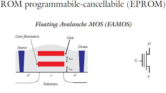
19 Cross-sections of NVM cells Flash Courtesy Intel EPROM
20 Read-Write Memories (RAM) STATIC (SRAM) Data stored as long as supply is applied Large (6 transistors/cell) Fast Differential DYNAMIC (DRAM) Periodic refresh required Small (1-3 transistors/cell) Slower Single Ended
21
22 6-transistor CMOS SRAM Cell WL V DD M 2 M 4 Q M Q M 5 6 M 1 M 3 BL BL
23
24
25
26 SRAM Characteristics
27 Esempio di organizzazione di una cella di memoria statica dato in selezione colonna S Q selezione riga R pass-gate (three state) dato out abilitazione scrittura abilitazione lettura
28 Esempio di organizzazione di una cella di memoria statica dato in dato in dato out selezione riga dato out dato in dato out abilitazione scrittura selezione colonna abilitazione lettura
29
30
31
32
33

34 BL 1 BL 2 WWL RWL WWL M 3 RWL M 1 C S X M 2 X BL1 V DD V DD - V T BL2 V DD - V T V
35 1-Transistor DRAM Cell WL BL WL Write 1 Read 1 M 1 X GND V DD 2 V T C S V DD BL V DD /2 V sensing DD /2 C BL Write: C S is charged or discharged by asserting WL and BL. Read: Charge redistribution takes places between bit line and storage capacitance Voltage swing is small; typically around 250 mv.
36
37 DRAM Cell Observations 1T DRAM requires a sense amplifier for each bit line, due to charge redistribution read-out. DRAM memory cells are single ended in contrast to SRAM cells. The read-out of the 1T DRAM cell is destructive; read and refresh operations are necessary for correct operation. Unlike 3T cell, 1T cell requires presence of an extra capacitance that must be explicitly included in the design. When writing a 1 into a DRAM cell, a threshold voltage is lost.
38 1-T DRAM Cell Metal word line Poly SiO 2 n + n + Field Oxide Poly Inversion layer induced by plate bias Cross-section Expensive in Area


39 Advanced 1T DRAM Cells Word line Insulating Layer Cell plate Capacitor dielectric layer Cell Plate Si Capacitor Insulator Refilling Poly Transfer gate Storage electrode Isolation Storage Node Poly 2nd Field Oxide Si Substrate Trench Cell Stacked-capacitor Cell
40 Periphery Decoders Sense Amplifiers Input/Output Buffers Control / Timing Circuitry
41 DRAM Timing
42 Reliability and Yield
43 Redundancy Redundant columns Redundant rows Memory Array Row Address Fuse : Bank Column Decoder Row Decoder Column Address
44 Error-Correcting Codes with e.g. B3 Wrong 1 1 = 3 0
45 Redundancy and Error Correction

46 125mm 2 1Gbit NAND Flash Memory 10.7mm Charge pump 2kB Page buffer & cache 32 word lines x 1024 blocks bit lines 11.7mm From [Nakamura02]
47 125mm 2 1Gbit NAND Flash Memory Technology 0.13 m p-sub CMOS triple-well 1poly, 1polycide, 1W, 2Al Cell size m2 Chip size 125.2mm2 Organization 2112 x 8b x 64 page x 1k block Power supply 2.7V-3.6V Cycle time 50ns Read time 25 s Program time 200 s / page Erase time 2ms / block From [Nakamura02]
EE141-Fall 2007 Digital Integrated Circuits. ROM and Flash. Announcements. Read-Only Memory Cells. Class Material. Semiconductor Memory Classification
 EE4-Fall 2007 igital Integrated Circuits Lecture 29 ROM, Flash, and RAM ROM and Flash 4 4 Announcements Final ec. 20 th Room TBA Final review sessions: Mon. ec. 7 th 3:30pm, 550 Cory Tues. ec. 7 th 3:30pm,
Semiconductor Memory Classification. Today. ESE 570: Digital Integrated Circuits and VLSI Fundamentals. CPU Memory Hierarchy.
 ESE 57: Digital Integrated Circuits and VLSI Fundamentals Lec : April 4, 7 Memory Overview, Memory Core Cells Today! Memory " Classification " ROM Memories " RAM Memory " Architecture " Memory core " SRAM
! Memory Overview. ! ROM Memories. ! RAM Memory " SRAM " DRAM. ! This is done because we can build. " large, slow memories OR
 ESE 57: Digital Integrated Circuits and VLSI Fundamentals Lec 2: April 5, 26 Memory Overview, Memory Core Cells Lecture Outline! Memory Overview! ROM Memories! RAM Memory " SRAM " DRAM 2 Memory Overview
EECS 427 Lecture 17: Memory Reliability and Power Readings: 12.4,12.5. EECS 427 F09 Lecture Reminders
 EECS 427 Lecture 17: Memory Reliability and Power Readings: 12.4,12.5 1 Reminders Deadlines HW4 is due Tuesday 11/17 at 11:59 pm (email submission) CAD8 is due Saturday 11/21 at 11:59 pm Quiz 2 is on Wednesday
Integrated Circuits & Systems
 Federal University of Santa Catarina Center for Technology Computer Science & Electronics Engineering Integrated Circuits & Systems INE 5442 Lecture 23-1 guntzel@inf.ufsc.br Semiconductor Memory Classification
! Memory. " RAM Memory. " Serial Access Memories. ! Cell size accounts for most of memory array size. ! 6T SRAM Cell. " Used in most commercial chips
 ESE 57: Digital Integrated Circuits and VLSI Fundamentals Lec : April 5, 8 Memory: Periphery circuits Today! Memory " RAM Memory " Architecture " Memory core " SRAM " DRAM " Periphery " Serial Access Memories
Memory Design I. Array-Structured Memory Architecture. Professor Chris H. Kim. Dept. of ECE.
 Memory Design I Professor Chris H. Kim University of Minnesota Dept. of ECE chriskim@ece.umn.edu Array-Structured Memory Architecture 2 1 Semiconductor Memory Classification Read-Write Wi Memory Non-Volatile
Semiconductor Memory Classification
 ESE37: Circuit-Level Modeling, Design, and Optimization for Digital Systems Lec 6: November, 7 Memory Overview Today! Memory " Classification " Architecture " Memory core " Periphery (time permitting)!
ESE370: Circuit-Level Modeling, Design, and Optimization for Digital Systems
 ESE370: Circuit-Level Modeling, Design, and Optimization for Digital Systems Lec 26: November 9, 2018 Memory Overview Dynamic OR4! Precharge time?! Driving input " With R 0 /2 inverter! Driving inverter
ECE321 Electronics I
 ECE321 Electronics I Lecture 28: DRAM & Flash Memories Payman Zarkesh-Ha Office: ECE Bldg. 230B Office hours: Tuesday 2:00-3:00PM or by appointment E-mail: payman@ece.unm.edu Slide: 1 Review of Last Lecture
CENG 4480 L09 Memory 2
 CENG 4480 L09 Memory 2 Bei Yu Reference: Chapter 11 Memories CMOS VLSI Design A Circuits and Systems Perspective by H.E.Weste and D.M.Harris 1 v.s. CENG3420 CENG3420: architecture perspective memory coherent
CMPEN 411 VLSI Digital Circuits Spring Lecture 22: Memery, ROM
 CMPEN 411 VLSI Digital Circuits Spring 2011 Lecture 22: Memery, ROM [Adapted from Rabaey s Digital Integrated Circuits, Second Edition, 2003 J. Rabaey, A. Chandrakasan, B. Nikolic] Sp11 CMPEN 411 L22 S.1
+1 (479)
") Memory Courtesy of Dr. Daehyun Lim@WSU, Dr. Harris@HMC, Dr. Shmuel Wimer@BIU and Dr. Choi@PSU http://csce.uark.edu +1 (479) 575-6043 yrpeng@uark.edu Memory Arrays Memory Arrays Random Access Memory Serial
Memory Courtesy of Dr. Daehyun Lim@WSU, Dr. Harris@HMC, Dr. Shmuel Wimer@BIU and Dr. Choi@PSU http://csce.uark.edu +1 (479) 575-6043 yrpeng@uark.edu Memory Arrays Memory Arrays Random Access Memory Serial
Based on slides/material by. Topic 7-4. Memory and Array Circuits. Outline. Semiconductor Memory Classification
 Based on slides/material by Topic 7 Memory and Array Circuits K. Masselos http://cas.ee.ic.ac.uk/~kostas J. Rabaey http://bwrc.eecs.berkeley.edu/classes/icbook/instructors.html Digital Integrated Circuits:
Memory Design I. Semiconductor Memory Classification. Read-Write Memories (RWM) Memory Scaling Trend. Memory Scaling Trend
 Memory Scaling Trend. Memory Scaling Trend") Array-Structured Memory Architecture Memory Design I Professor hris H. Kim University of Minnesota Dept. of EE chriskim@ece.umn.edu 2 Semiconductor Memory lassification Read-Write Memory Non-Volatile Read-Write
Array-Structured Memory Architecture Memory Design I Professor hris H. Kim University of Minnesota Dept. of EE chriskim@ece.umn.edu 2 Semiconductor Memory lassification Read-Write Memory Non-Volatile Read-Write
Memory and Programmable Logic
 Digital Circuit Design and Language Memory and Programmable Logic Chang, Ik Joon Kyunghee University Memory Classification based on functionality ROM : Read-Only Memory RWM : Read-Write Memory RWM NVRWM
COMP3221: Microprocessors and. and Embedded Systems. Overview. Lecture 23: Memory Systems (I)
") COMP3221: Microprocessors and Embedded Systems Lecture 23: Memory Systems (I) Overview Memory System Hierarchy RAM, ROM, EPROM, EEPROM and FLASH http://www.cse.unsw.edu.au/~cs3221 Lecturer: Hui Wu Session
COMP3221: Microprocessors and Embedded Systems Lecture 23: Memory Systems (I) Overview Memory System Hierarchy RAM, ROM, EPROM, EEPROM and FLASH http://www.cse.unsw.edu.au/~cs3221 Lecturer: Hui Wu Session
! Serial Access Memories. ! Multiported SRAM ! 5T SRAM ! DRAM. ! Shift registers store and delay data. ! Simple design: cascade of registers
 ESE370: Circuit-Level Modeling, Design, and Optimization for Digital Systems Lec 28: November 16, 2016 RAM Core Pt 2 Outline! Serial Access Memories! Multiported SRAM! 5T SRAM! DRAM Penn ESE 370 Fall 2016
Memory. Outline. ECEN454 Digital Integrated Circuit Design. Memory Arrays. SRAM Architecture DRAM. Serial Access Memories ROM
 ECEN454 Digital Integrated Circuit Design Memory ECEN 454 Memory Arrays SRAM Architecture SRAM Cell Decoders Column Circuitry Multiple Ports DRAM Outline Serial Access Memories ROM ECEN 454 12.2 1 Memory
ENEE 759H, Spring 2005 Memory Systems: Architecture and
 SLIDE, Memory Systems: DRAM Device Circuits and Architecture Credit where credit is due: Slides contain original artwork ( Jacob, Wang 005) Overview Processor Processor System Controller Memory Controller
Advanced 1 Transistor DRAM Cells
 Trench DRAM Cell Bitline Wordline n+ - Si SiO 2 Polysilicon p-si Depletion Zone Inversion at SiO 2 /Si Interface [IC1] Address Transistor Memory Capacitor SoC - Memory - 18 Advanced 1 Transistor DRAM Cells
CMOS Logic Circuit Design Link( リンク ): センター教官講義ノートの下 CMOS 論理回路設計
: センター教官講義ノートの下 CMOS 論理回路設計") CMOS Logic Circuit Design http://www.rcns.hiroshima-u.ac.jp Link( リンク ): センター教官講義ノートの下 CMOS 論理回路設計 Memory Circuits (Part 1) Overview of Memory Types Memory with Address-Based Access Principle of Data Access
CMOS Logic Circuit Design http://www.rcns.hiroshima-u.ac.jp Link( リンク ): センター教官講義ノートの下 CMOS 論理回路設計 Memory Circuits (Part 1) Overview of Memory Types Memory with Address-Based Access Principle of Data Access
Very Large Scale Integration (VLSI)
") Very Large Scale Integration (VLSI) Lecture 8 Dr. Ahmed H. Madian ah_madian@hotmail.com Content Array Subsystems Introduction General memory array architecture SRAM (6-T cell) CAM Read only memory Introduction
Very Large Scale Integration (VLSI) Lecture 8 Dr. Ahmed H. Madian ah_madian@hotmail.com Content Array Subsystems Introduction General memory array architecture SRAM (6-T cell) CAM Read only memory Introduction
Module 6 : Semiconductor Memories Lecture 30 : SRAM and DRAM Peripherals
 Module 6 : Semiconductor Memories Lecture 30 : SRAM and DRAM Peripherals Objectives In this lecture you will learn the following Introduction SRAM and its Peripherals DRAM and its Peripherals 30.1 Introduction
Concept of Memory. The memory of computer is broadly categories into two categories:
 Concept of Memory We have already mentioned that digital computer works on stored programmed concept introduced by Von Neumann. We use memory to store the information, which includes both program and data.
Lecture 13: SRAM. Slides courtesy of Deming Chen. Slides based on the initial set from David Harris. 4th Ed.
 Lecture 13: SRAM Slides courtesy of Deming Chen Slides based on the initial set from David Harris CMOS VLSI Design Outline Memory Arrays SRAM Architecture SRAM Cell Decoders Column Circuitry Multiple Ports
Chapter 5 Internal Memory
 Chapter 5 Internal Memory Memory Type Category Erasure Write Mechanism Volatility Random-access memory (RAM) Read-write memory Electrically, byte-level Electrically Volatile Read-only memory (ROM) Read-only
Computer Organization. 8th Edition. Chapter 5 Internal Memory
 William Stallings Computer Organization and Architecture 8th Edition Chapter 5 Internal Memory Semiconductor Memory Types Memory Type Category Erasure Write Mechanism Volatility Random-access memory (RAM)
Organization. 5.1 Semiconductor Main Memory. William Stallings Computer Organization and Architecture 6th Edition
 William Stallings Computer Organization and Architecture 6th Edition Chapter 5 Internal Memory 5.1 Semiconductor Main Memory 5.2 Error Correction 5.3 Advanced DRAM Organization 5.1 Semiconductor Main Memory
CHAPTER 12 ARRAY SUBSYSTEMS [ ] MANJARI S. KULKARNI
![CHAPTER 12 ARRAY SUBSYSTEMS [ ] MANJARI S. KULKARNI](/thumbs/76/73997056.jpg "CHAPTER 12 ARRAY SUBSYSTEMS [ ] MANJARI S. KULKARNI") CHAPTER 2 ARRAY SUBSYSTEMS [2.4-2.9] MANJARI S. KULKARNI OVERVIEW Array classification Non volatile memory Design and Layout Read-Only Memory (ROM) Pseudo nmos and NAND ROMs Programmable ROMS PROMS, EPROMs,
CHAPTER 2 ARRAY SUBSYSTEMS [2.4-2.9] MANJARI S. KULKARNI OVERVIEW Array classification Non volatile memory Design and Layout Read-Only Memory (ROM) Pseudo nmos and NAND ROMs Programmable ROMS PROMS, EPROMs,
William Stallings Computer Organization and Architecture 6th Edition. Chapter 5 Internal Memory
 William Stallings Computer Organization and Architecture 6th Edition Chapter 5 Internal Memory Semiconductor Memory Types Semiconductor Memory RAM Misnamed as all semiconductor memory is random access
Introduction to SRAM. Jasur Hanbaba
 Introduction to SRAM Jasur Hanbaba Outline Memory Arrays SRAM Architecture SRAM Cell Decoders Column Circuitry Non-volatile Memory Manufacturing Flow Memory Arrays Memory Arrays Random Access Memory Serial
Memory Arrays. Array Architecture. Chapter 16 Memory Circuits and Chapter 12 Array Subsystems from CMOS VLSI Design by Weste and Harris, 4 th Edition
 Chapter 6 Memory Circuits and Chapter rray Subsystems from CMOS VLSI Design by Weste and Harris, th Edition E E 80 Introduction to nalog and Digital VLSI Paul M. Furth New Mexico State University Static
Basic Organization Memory Cell Operation. CSCI 4717 Computer Architecture. ROM Uses. Random Access Memory. Semiconductor Memory Types
 CSCI 4717/5717 Computer Architecture Topic: Internal Memory Details Reading: Stallings, Sections 5.1 & 5.3 Basic Organization Memory Cell Operation Represent two stable/semi-stable states representing
William Stallings Computer Organization and Architecture 8th Edition. Chapter 5 Internal Memory
 William Stallings Computer Organization and Architecture 8th Edition Chapter 5 Internal Memory Semiconductor Memory The basic element of a semiconductor memory is the memory cell. Although a variety of
Internal Memory. Computer Architecture. Outline. Memory Hierarchy. Semiconductor Memory Types. Copyright 2000 N. AYDIN. All rights reserved.
 Computer Architecture Prof. Dr. Nizamettin AYDIN naydin@yildiz.edu.tr nizamettinaydin@gmail.com Internal Memory http://www.yildiz.edu.tr/~naydin 1 2 Outline Semiconductor main memory Random Access Memory
Introduction to CMOS VLSI Design. Semiconductor Memory Harris and Weste, Chapter October 2018
 Introduction to CMOS VLSI Design Semiconductor Memory Harris and Weste, Chapter 12 25 October 2018 J. J. Nahas and P. M. Kogge Modified from slides by Jay Brockman 2008 [Including slides from Harris &
ECSE-2610 Computer Components & Operations (COCO)
") ECSE-2610 Computer Components & Operations (COCO) Part 18: Random Access Memory 1 Read-Only Memories 2 Why ROM? Program storage Boot ROM for personal computers Complete application storage for embedded
ECSE-2610 Computer Components & Operations (COCO) Part 18: Random Access Memory 1 Read-Only Memories 2 Why ROM? Program storage Boot ROM for personal computers Complete application storage for embedded
CENG 4480 L09 Memory 3
 CENG 4480 L09 Memory 3 Bei Yu Chapter 11 Memories Reference: CMOS VLSI Design A Circuits and Systems Perspective by H.E.Weste and D.M.Harris 1 Memory Arrays Memory Arrays Random Access Memory Serial Access
Microcontroller Systems. ELET 3232 Topic 11: General Memory Interfacing
 Microcontroller Systems ELET 3232 Topic 11: General Memory Interfacing 1 Objectives To become familiar with the concepts of memory expansion and the data and address bus To design embedded systems circuits
ELCT 912: Advanced Embedded Systems
 Advanced Embedded Systems Lecture 2: Memory and Programmable Logic Dr. Mohamed Abd El Ghany, Memory Random Access Memory (RAM) Can be read and written Static Random Access Memory (SRAM) Data stored so
Digital Systems. Semiconductor memories. Departamentul de Bazele Electronicii
 Digital Systems Semiconductor memories Departamentul de Bazele Electronicii Outline ROM memories ROM memories PROM memories EPROM memories EEPROM, Flash, MLC memories Applications with ROM memories extending
Lecture 11 SRAM Zhuo Feng. Z. Feng MTU EE4800 CMOS Digital IC Design & Analysis 2010
 EE4800 CMOS Digital IC Design & Analysis Lecture 11 SRAM Zhuo Feng 11.1 Memory Arrays SRAM Architecture SRAM Cell Decoders Column Circuitryit Multiple Ports Outline Serial Access Memories 11.2 Memory Arrays
Embedded Systems Design: A Unified Hardware/Software Introduction. Outline. Chapter 5 Memory. Introduction. Memory: basic concepts
 Hardware/Software Introduction Chapter 5 Memory Outline Memory Write Ability and Storage Permanence Common Memory Types Composing Memory Memory Hierarchy and Cache Advanced RAM 1 2 Introduction Memory:
Embedded Systems Design: A Unified Hardware/Software Introduction. Chapter 5 Memory. Outline. Introduction
 Hardware/Software Introduction Chapter 5 Memory 1 Outline Memory Write Ability and Storage Permanence Common Memory Types Composing Memory Memory Hierarchy and Cache Advanced RAM 2 Introduction Embedded
COMPUTER ARCHITECTURE
 COMPUTER ARCHITECTURE 8 Memory Types & Technologies RA - 8 2018, Škraba, Rozman, FRI Memory types & technologies - objectives 8 Memory types & technologies - objectives: Basic understanding of: The speed
Chapter 3 Semiconductor Memories. Jin-Fu Li Department of Electrical Engineering National Central University Jungli, Taiwan
 Chapter 3 Semiconductor Memories Jin-Fu Li Department of Electrical Engineering National Central University Jungli, Taiwan Outline Introduction Random Access Memories Content Addressable Memories Read
SRAM. Introduction. Digital IC
 SRAM Introduction Outline Memory Arrays SRAM Architecture SRAM Cell Decoders Column Circuitry Multiple Ports Serial Access Memories Memory Arrays Memory Arrays Random Access Memory Serial Access Memory
Sense Amplifiers 6 T Cell. M PC is the precharge transistor whose purpose is to force the latch to operate at the unstable point.
 Announcements (Crude) notes for switching speed example from lecture last week posted. Schedule Final Project demo with TAs. Written project report to include written evaluation section. Send me suggestions
Introduction to Semiconductor Memory Dr. Lynn Fuller Webpage:
 ROCHESTER INSTITUTE OF TECHNOLOGY MICROELECTRONIC ENGINEERING Introduction to Semiconductor Memory Webpage: http://people.rit.edu/lffeee 82 Lomb Memorial Drive Rochester, NY 14623-5604 Tel (585) 475-2035
P-2 Digital Design & Applications
 P-2 Digital Design & Applications Semiconductor Memory (Unit-V) By: A K Verma SOS in Electronics & Photonics Pt. Ravishankar Shukla University, Raipur (C.G.) 1 What is Memory? In computing, memory refers
Design with Microprocessors
 Design with Microprocessors Year III Computer Sci. English 1-st Semester Lecture 12: Memory interfacing Typical Memory Hierarchy [1] On-Chip Components Control edram Datapath RegFile ITLB DTLB Instr Data
Hardware Design with VHDL PLDs I ECE 443. FPGAs can be configured at least once, many are reprogrammable.
 PLDs, ASICs and FPGAs FPGA definition: Digital integrated circuit that contains configurable blocks of logic and configurable interconnects between these blocks. Key points: Manufacturer does NOT determine
Design with Microprocessors
 Design with Microprocessors Year III Computer Sci. English 1-st Semester Lecture 12: Memory interfacing Typical Memory Hierarchy [1] On-Chip Components Control edram Datapath RegFile ITLB DTLB Instr Data
(Advanced) Computer Organization & Architechture. Prof. Dr. Hasan Hüseyin BALIK (5 th Week)
 Computer Organization & Architechture. Prof. Dr. Hasan Hüseyin BALIK (5 th Week)") + (Advanced) Computer Organization & Architechture Prof. Dr. Hasan Hüseyin BALIK (5 th Week) + Outline 2. The computer system 2.1 A Top-Level View of Computer Function and Interconnection 2.2 Cache Memory
+ (Advanced) Computer Organization & Architechture Prof. Dr. Hasan Hüseyin BALIK (5 th Week) + Outline 2. The computer system 2.1 A Top-Level View of Computer Function and Interconnection 2.2 Cache Memory
Read and Write Cycles
 Read and Write Cycles The read cycle is shown. Figure 41.1a. The RAS and CAS signals are activated one after the other to latch the multiplexed row and column addresses respectively applied at the multiplexed
The Memory Hierarchy Part I
 Chapter 6 The Memory Hierarchy Part I The slides of Part I are taken in large part from V. Heuring & H. Jordan, Computer Systems esign and Architecture 1997. 1 Outline: Memory components: RAM memory cells
Introduction to CMOS VLSI Design Lecture 13: SRAM
 Introduction to CMOS VLSI Design Lecture 13: SRAM David Harris Harvey Mudd College Spring 2004 1 Outline Memory Arrays SRAM Architecture SRAM Cell Decoders Column Circuitry Multiple Ports Serial Access
ECEN 449 Microprocessor System Design. Memories
 ECEN 449 Microprocessor System Design Memories 1 Objectives of this Lecture Unit Learn about different types of memories SRAM/DRAM/CAM /C Flash 2 1 SRAM Static Random Access Memory 3 SRAM Static Random
Chapter Two - SRAM 1. Introduction to Memories. Static Random Access Memory (SRAM)
") 1 3 Introduction to Memories The most basic classification of a memory device is whether it is Volatile or Non-Volatile (NVM s). These terms refer to whether or not a memory device loses its contents when
1 3 Introduction to Memories The most basic classification of a memory device is whether it is Volatile or Non-Volatile (NVM s). These terms refer to whether or not a memory device loses its contents when
CS 320 February 2, 2018 Ch 5 Memory
 CS 320 February 2, 2018 Ch 5 Memory Main memory often referred to as core by the older generation because core memory was a mainstay of computers until the advent of cheap semi-conductor memory in the
Digital Integrated Circuits Lecture 13: SRAM
 Digital Integrated Circuits Lecture 13: SRAM Chih-Wei Liu VLSI Signal Processing LAB National Chiao Tung University cwliu@twins.ee.nctu.edu.tw DIC-Lec13 cwliu@twins.ee.nctu.edu.tw 1 Outline Memory Arrays
Chapter 4 Main Memory
 Chapter 4 Main Memory Course Outcome (CO) - CO2 Describe the architecture and organization of computer systems Program Outcome (PO) PO1 Apply knowledge of mathematics, science and engineering fundamentals
UMBC. Select. Read. Write. Output/Input-output connection. 1 (Feb. 25, 2002) Four commonly used memories: Address connection ... Dynamic RAM (DRAM)
 Four commonly used memories: Address connection ... Dynamic RAM (DRAM)") Memory Types Two basic types: ROM: Read-only memory RAM: Read-Write memory Four commonly used memories: ROM Flash (EEPROM) Static RAM (SRAM) Dynamic RAM (DRAM) Generic pin configuration: Address connection
Memory Types Two basic types: ROM: Read-only memory RAM: Read-Write memory Four commonly used memories: ROM Flash (EEPROM) Static RAM (SRAM) Dynamic RAM (DRAM) Generic pin configuration: Address connection
Information Storage and Spintronics 10
 Information Storage and Spintronics 10 Atsufumi Hirohata Department of Electronic Engineering 09:00 Tuesday, 30/October/2018 (J/Q 004) Quick Review over the Last Lecture Flash memory : NAND-flash writing
CREATED BY M BILAL & Arslan Ahmad Shaad Visit:
 CREATED BY M BILAL & Arslan Ahmad Shaad Visit: www.techo786.wordpress.com Q1: Define microprocessor? Short Questions Chapter No 01 Fundamental Concepts Microprocessor is a program-controlled and semiconductor
Memory classification:- Topics covered:- types,organization and working
 Memory classification:- Topics covered:- types,organization and working 1 Contents What is Memory? Cache Memory PC Memory Organisation Types 2 Memory what is it? Usually we consider this to be RAM, ROM
Address connections Data connections Selection connections
 Interface (cont..) We have four common types of memory: Read only memory ( ROM ) Flash memory ( EEPROM ) Static Random access memory ( SARAM ) Dynamic Random access memory ( DRAM ). Pin connections common
MEMORIES. Memories. EEC 116, B. Baas 3
 MEMORIES Memories VLSI memories can be classified as belonging to one of two major categories: Individual registers, single bit, or foreground memories Clocked: Transparent latches and Flip-flops Unclocked:
Views of Memory. Real machines have limited amounts of memory. Programmer doesn t want to be bothered. 640KB? A few GB? (This laptop = 2GB)
") CS6290 Memory Views of Memory Real machines have limited amounts of memory 640KB? A few GB? (This laptop = 2GB) Programmer doesn t want to be bothered Do you think, oh, this computer only has 128MB so
CS6290 Memory Views of Memory Real machines have limited amounts of memory 640KB? A few GB? (This laptop = 2GB) Programmer doesn t want to be bothered Do you think, oh, this computer only has 128MB so
Design and Implementation of an AHB SRAM Memory Controller
 Design and Implementation of an AHB SRAM Memory Controller 1 Module Overview Learn the basics of Computer Memory; Design and implement an AHB SRAM memory controller, which replaces the previous on-chip
chapter 8 The Memory System Chapter Objectives
 chapter 8 The Memory System Chapter Objectives In this chapter you will learn about: Basic memory circuits Organization of the main memory Memory technology Direct memory access as an I/O mechanism Cache
MTJ-Based Nonvolatile Logic-in-Memory Architecture
 2011 Spintronics Workshop on LSI @ Kyoto, Japan, June 13, 2011 MTJ-Based Nonvolatile Logic-in-Memory Architecture Takahiro Hanyu Center for Spintronics Integrated Systems, Tohoku University, JAPAN Laboratory
MEMORY BHARAT SCHOOL OF BANKING- VELLORE
 A memory is just like a human brain. It is used to store data and instructions. Computer memory is the storage space in computer where data is to be processed and instructions required for processing are
ECE 152 Introduction to Computer Architecture
 Introduction to Computer Architecture Main Memory and Virtual Memory Copyright 2009 Daniel J. Sorin Duke University Slides are derived from work by Amir Roth (Penn) Spring 2009 1 Where We Are in This Course
ECE 2300 Digital Logic & Computer Organization
 ECE 2300 Digital Logic & Computer Organization Spring 201 Memories Lecture 14: 1 Announcements HW6 will be posted tonight Lab 4b next week: Debug your design before the in-lab exercise Lecture 14: 2 Review:
8051 INTERFACING TO EXTERNAL MEMORY
 8051 INTERFACING TO EXTERNAL MEMORY Memory Capacity The number of bits that a semiconductor memory chip can store Called chip capacity It can be in units of Kbits (kilobits), Mbits (megabits), and so on
Memory in Digital Systems
 MEMORIES Memory in Digital Systems Three primary components of digital systems Datapath (does the work) Control (manager) Memory (storage) Single bit ( foround ) Clockless latches e.g., SR latch Clocked
NAND Flash Memory. Jinkyu Jeong Computer Systems Laboratory Sungkyunkwan University
 NAND Flash Memory Jinkyu Jeong (Jinkyu@skku.edu) Computer Systems Laboratory Sungkyunkwan University http://csl.skku.edu ICE3028: Embedded Systems Design, Fall 2018, Jinkyu Jeong (jinkyu@skku.edu) Flash
CSE502: Computer Architecture CSE 502: Computer Architecture
 CSE 502: Computer Architecture Memory / DRAM SRAM = Static RAM SRAM vs. DRAM As long as power is present, data is retained DRAM = Dynamic RAM If you don t do anything, you lose the data SRAM: 6T per bit
ECE 485/585 Microprocessor System Design
 Microprocessor System Design Lecture 4: Memory Hierarchy Memory Taxonomy SRAM Basics Memory Organization DRAM Basics Zeshan Chishti Electrical and Computer Engineering Dept Maseeh College of Engineering
Introduction read-only memory random access memory
 Memory Interface Introduction Simple or complex, every microprocessorbased system has a memory system. Almost all systems contain two main types of memory: read-only memory (ROM) and random access memory
PROGRAMMABLE MODULES SPECIFICATION OF PROGRAMMABLE COMBINATIONAL AND SEQUENTIAL MODULES
 PROGRAMMABLE MODULES SPECIFICATION OF PROGRAMMABLE COMBINATIONAL AND SEQUENTIAL MODULES. psa. rom. fpga THE WAY THE MODULES ARE PROGRAMMED NETWORKS OF PROGRAMMABLE MODULES EXAMPLES OF USES Programmable
ECEN 449 Microprocessor System Design. Memories. Texas A&M University
 ECEN 449 Microprocessor System Design Memories 1 Objectives of this Lecture Unit Learn about different types of memories SRAM/DRAM/CAM Flash 2 SRAM Static Random Access Memory 3 SRAM Static Random Access
Chapter 8 Memory Basics
 Logic and Computer Design Fundamentals Chapter 8 Memory Basics Charles Kime & Thomas Kaminski 2008 Pearson Education, Inc. (Hyperlinks are active in View Show mode) Overview Memory definitions Random Access
The Memory Hierarchy 1
 The Memory Hierarchy 1 What is a cache? 2 What problem do caches solve? 3 Memory CPU Abstraction: Big array of bytes Memory memory 4 Performance vs 1980 Processor vs Memory Performance Memory is very slow
Z-RAM Ultra-Dense Memory for 90nm and Below. Hot Chips David E. Fisch, Anant Singh, Greg Popov Innovative Silicon Inc.
 Z-RAM Ultra-Dense Memory for 90nm and Below Hot Chips 2006 David E. Fisch, Anant Singh, Greg Popov Innovative Silicon Inc. Outline Device Overview Operation Architecture Features Challenges Z-RAM Performance
Programmable Logic Devices Introduction CMPE 415. Programmable Logic Devices
 Instructor: Professor Jim Plusquellic Programmable Logic Devices Text: The Design Warrior s Guide to FPGAs, Devices, Tools and Flows, Clive "Max" Maxfield, ISBN: 0-7506-7604-3 Modeling, Synthesis and Rapid
Memory in Digital Systems
 MEMORIES Memory in Digital Systems Three primary components of digital systems Datapath (does the work) Control (manager) Memory (storage) Single bit ( foround ) Clockless latches e.g., SR latch Clocked
Digital Integrated Circuits (83-313) Lecture 7: SRAM. Semester B, Lecturer: Dr. Adam Teman Itamar Levi, Robert Giterman.
 Lecture 7: SRAM. Semester B, Lecturer: Dr. Adam Teman Itamar Levi, Robert Giterman.") Digital Integrated Circuits (83-313) Lecture 7: SRAM Semester B, 2016-17 Lecturer: Dr. Adam Teman TAs: Itamar Levi, Robert Giterman 16 May 2017 Disclaimer: This course was prepared, in its entirety, by
Digital Integrated Circuits (83-313) Lecture 7: SRAM Semester B, 2016-17 Lecturer: Dr. Adam Teman TAs: Itamar Levi, Robert Giterman 16 May 2017 Disclaimer: This course was prepared, in its entirety, by
Semiconductor Memories: RAMs and ROMs
 Semiconductor Memories: RAMs and ROMs Lesson Objectives: In this lesson you will be introduced to: Different memory devices like, RAM, ROM, PROM, EPROM, EEPROM, etc. Different terms like: read, write,
ECE 341. Lecture # 16
 ECE 341 Lecture # 16 Instructor: Zeshan Chishti zeshan@ece.pdx.edu November 24, 2014 Portland State University Lecture Topics The Memory System Basic Concepts Semiconductor RAM Memories Organization of
Memory technology and optimizations ( 2.3) Main Memory
 Main Memory") Memory technology and optimizations ( 2.3) 47 Main Memory Performance of Main Memory: Latency: affects Cache Miss Penalty» Access Time: time between request and word arrival» Cycle Time: minimum time between
Memory technology and optimizations ( 2.3) 47 Main Memory Performance of Main Memory: Latency: affects Cache Miss Penalty» Access Time: time between request and word arrival» Cycle Time: minimum time between
Memory Expansion. Lecture Embedded Systems
 Memory Expansion Lecture 22 22-1 In These Notes... Memory Types Memory Expansion Interfacing Parallel Serial Direct Memory Access controllers 22-2 Memory Characteristics and Issues Volatility - Does it
UNIT:4 MEMORY ORGANIZATION
 1 UNIT:4 MEMORY ORGANIZATION TOPICS TO BE COVERED. 4.1 Memory Hierarchy 4.2 Memory Classification 4.3 RAM,ROM,PROM,EPROM 4.4 Main Memory 4.5Auxiliary Memory 4.6 Associative Memory 4.7 Cache Memory 4.8
Flash Memories. Ramin Roosta Dept. of Computer Engineering. EE 595 EDA / ASIC Design Lab
 Flash Memories Ramin Roosta Dept. of Computer Engineering EE 595 EDA / ASIC Design Lab Content Non-volatile memories Flash applications Industry standards Architectures Main reliability issues New cells
Multilevel Memories. Joel Emer Computer Science and Artificial Intelligence Laboratory Massachusetts Institute of Technology
 1 Multilevel Memories Computer Science and Artificial Intelligence Laboratory Massachusetts Institute of Technology Based on the material prepared by Krste Asanovic and Arvind CPU-Memory Bottleneck 6.823
Chapter 5. Internal Memory. Yonsei University
 Chapter 5 Internal Memory Contents Main Memory Error Correction Advanced DRAM Organization 5-2 Memory Types Memory Type Category Erasure Write Mechanism Volatility Random-access memory(ram) Read-write
The DRAM Cell. EEC 581 Computer Architecture. Memory Hierarchy Design (III) 1T1C DRAM cell
 1T1C DRAM cell") EEC 581 Computer Architecture Memory Hierarchy Design (III) Department of Electrical Engineering and Computer Science Cleveland State University The DRAM Cell Word Line (Control) Bit Line (Information)
EEC 581 Computer Architecture Memory Hierarchy Design (III) Department of Electrical Engineering and Computer Science Cleveland State University The DRAM Cell Word Line (Control) Bit Line (Information)
ΔΙΑΛΕΞΗ 5: FPGA Programming Technologies (aka: how to connect/disconnect wires/gates)
") ΗΜΥ 408 ΨΗΦΙΑΚΟΣ ΣΧΕΔΙΑΣΜΟΣ ΜΕ FPGAs Χειμερινό Εξάμηνο 2018 ΔΙΑΛΕΞΗ 5: FPGA Programming Technologies (aka: how to connect/disconnect wires/gates) (ack: Jurriaan Schmitz, Semiconductor Components) ΧΑΡΗΣ
ΗΜΥ 408 ΨΗΦΙΑΚΟΣ ΣΧΕΔΙΑΣΜΟΣ ΜΕ FPGAs Χειμερινό Εξάμηνο 2018 ΔΙΑΛΕΞΗ 5: FPGA Programming Technologies (aka: how to connect/disconnect wires/gates) (ack: Jurriaan Schmitz, Semiconductor Components) ΧΑΡΗΣ