Programable Logic Devices
|
|
|
- Marjory Felicia Gibson
- 5 years ago
- Views:
Transcription
1 Programable Logic Devices In the 1970s programmable logic circuits called programmable logic device (PLD) was introduced. They are based on a structure with an AND- OR array that makes it easy to implement SOP expression
2 PLD structure x 1 x 2 x n Input buffers and inverters x 1 x 1 x n x n P 1 AND plane P k OR plane f 1 f m
3 Programmable Logic Array (PLA) x 1 x 2 x 3 Both AND and OR arrays are programmable P 1 OR plane P 2 P 3 P 4 AND plane f f
4 Programmable Array Logic (PAL) x 1 x 2 x 3 Only the AND array is programmable P 1 P 2 f 1 P 3 P 4 f 2 AND plane
5 Register output In the earlier PLD circuits there were combinatorial outputs register outputs (output with a flip-flop) For each circuit there were a fixed number of combinational and register outputs To increase flexibility the macrocell where you could choose if an output would be a combinatorial or a register output was introduced.
6 Macrocels ia a PLD Select Enable Flip-flop f 1 Clock D Q With a programmable multiplexer one can select the type of output To AND plane
7 PAL
8 Programing of PLDs
9 Complex PLDs (CPLD) PLD were quite small (PALCE 22V10 had 10 flip-flops) For bigger programmable circuits a structure consisting of several PLD-like block was developed.
10 CPLD (MAX)
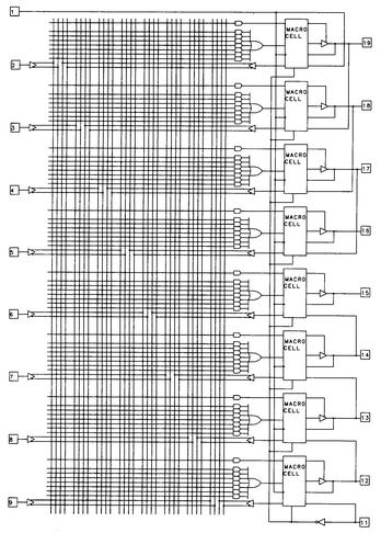
11 CPLD structure I/O block PAL-like block PAL-like block I/O block Interconnection wires I/O block PAL-like block PAL-like block I/O block
12 Programing with JTAG Modern CPLDs (and FPGAs) can be programmed by downloading programming information via a cable Download will usually use a standard port: JTAG-port

13 JTAG programing (a) CPLD in a Quad Flat Pack (QFP) package To computer You can program the chips when they are soldered to the circuit board - from inside the programmer you can select which chip you want to program with the JTAG connector. Printed circuit board (b) JTAG programming
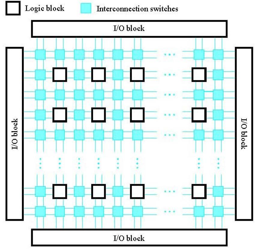
14 FPGA chips CPLD:s are based on the AND-OR array, and it becomes difficult to make really large circuits FPGA (Field Programmable Gate Array) circuits using a different concept based on logical blocks
15 FPGA-structure
16 LUT-LookUp-Table Programmable cells 0/1 0/1 0/ f A LUT with n inputs can realize all combinational functions with n inputs. The usual size in an FPGA is n=4 0/1 0 x 2 x 1 Two-input LUT
17 Ex. LUT for XOR-gate x2 x1 f f x 2 x 1 Two-input LUT
18 Logic block in FPGA A logic block of an FPGA consists of a LUT, a flipflop, and a mux to select register output. Select In 1 Flip-flop Out In 2 LUT D Q In 3 Clock
19 Interconnexion matrix in FPGA x 3 f Blue cross: connection is programmed Black cross: connection is not programmed x 1 x 2 x 1 x x 2 0 f 1 1 f x f 1 f f

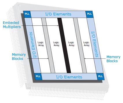
20 DE2 University Board Cyclone II EP2C35 FPGA Datorteknikcourse
21 Cyclone II logic element
22 Cyclone II Family (3) Total Number of 18x18 Multipliers DE2

23 Stratix III Family DE3 Board
24 Multiple processors on an FPGA Nios II is a so-called 'softprocessor' (32-bit) which can be implemented on an Altera FPGA Today's FPGAs are so large that multiple processors can fit on a single FPGA chip Nios II Nios II Very powerful multiprocessor systems can be created on an FPGA!
25 ASIC An ASIC (Application Specific Integrated Circuit) is a circuit that is madi in a semiconductor factory In a full custom integrated circuit you in principle tailors the whole circuit In an ASIC have certain work steps already been made to reduce design time and cost
 are allready on the silicon.")
26 ASIC, gate array In an Gate Array the gates (or transistors) are allready on the silicon.
27 ASIC, gate array f 1 One only creates links between inputs, gates, and outputs x 1 x 2 x 3
28 Comparison ASIC, FPGA Initial Cost Cost per part Performance Fabrication Time FPGA Low High Low Short Gate Array (ASIC) Standard Cell (ASIC) High Low High Long
29 Design Trade-Offs Design Time Full Custom Standard Cell Gate Array Programmable Logic Microprocessor Performance
30
31 Sekvenskretsar med VHDL State Inputsignals NEXT STATE DECODER STATE REGISTER OUTPUT DECODER Outputsignals Clk Moore-machine
32 Model a State Machine in VHDL In a Moore-machine we have three blocks Next-state-decoder Output-decoder State-register These blocks execute in parallel
33 Quickie Question which logic gate corresponds to the following VHDL code
34 Quickie Question which logic gate corresponds to the following VHDL code
35 Quickie Question which logic gate corresponds to the following VHDL code
36 Quickie Question which logic gate corresponds to the following VHDL code
37 Processes in VHDL An architecture in VHDL can consist of several processes Processes are executed in parallel A process is written as a sequential program
38 Moore-machine processes For a Moore-machine, we can create three processes Next-state-decoder Output-decoder State-register
39 Internal signals Moore-machine contains internal signals Next state Present state Theese signals are declared in the architecture-description

40 The vending machine in VHDL We use bottle vending machine (system control) from last lecture as a concrete VHDL example COIN RECEIVER COIN_PRESENT GT_1_EURO EQ_1_EURO LT_1_EURO SYSTEM CONTROL DROP DROP_READY DROP BOTTLE ACCUMU- LATOR DEC_ACC CLR_ACC RETURN_10_CENT CHANGER_READY COIN RETURN
41 COIN_PRESENT GT_1_EURO EQ_1_EURO LT_1_EURO DEC_ACC CLR_ACC Reset_n Clk Vending machine entity SYSTEM CONTROL DROP DROP_READY Clk and Reset (active low) is also needed! RETURN_10_CENT CHANGER_READY ENTITY Vending_Machine IS PORT ( -- Inputs coin_present gt_1_euro eq_1_euro lt_1_euro drop_ready : IN std_logic; : IN std_logic; : IN std_logic; : IN std_logic; : IN std_logic; changer_ready : IN std_logic; reset_n clk -- Outputs dec_acc clr_acc drop : IN std_logic; : IN std_logic; : OUT std_logic; : OUT std_logic; : OUT std_logic; return_10_cent : OUT std_logic); END Vending_Machine;
42 Vending machine architecture The architecture describes the function of the vending machine We define internal signals for present and next state three processes for next-statedecoder, output-decoder and stateregister
43 State diagram (a) Wait for coin input (b) Register the coin (c) Coin is registered (3 cases) (d) Drop bottle (e) Reset sum (f) Return 10 Cent (g) Decrement sum with 10 Cent
44 Internal signals We need to create a data type for the internal signal Since we describe the states we use an enumeration type with values a,b,c,d,e,f,g We declare a variable for the current state (current_state) and one for next state (next_state) ARCHITECTURE Moore_FSM OF Vending_Machine IS TYPE state_type IS (a, b, c, d, e, f, g); SIGNAL current_state, next_state : state_type; BEGIN -- Moore_FSM
45 We want to keep our "clever state encoding If we do not specify the encoding state then the synthesis tool chooses the coding. We can force it to a specific encoding with attributes (NOTE Attributes are dependent on synthesis tool and thus not portable!) ARCHITECTURE Moore_FSM OF Vending_Machine IS TYPE state_type IS (a, b, c, d, e, f, g); -- We can use state encoding according to BV to enforce a particular encoding (for Quartus) ATTRIBUTE enum_encoding : string; ATTRIBUTE enum_encoding OF state_type : TYPE IS " "; SIGNAL current_state, next_state BEGIN -- Moore_FSM : state_type;
46 COIN_PRESENT LT_I_EURO EQ_I_EURO GT_I_EURO DROP_READY CHANGER_READY Block schematic Next State Decoder D A Clk D B Clk D D A B Output Decoder DROP RETURN_I0_CENT CLR_ACC A B D C D C DEC_ACC C Clk Signals A,B,C describes present state Signals D A, D B, D C describes next state
47 Quickie Question which statemachine corresponds to the VHDL code
48 Quickie Question which statemachine corresponds to the VHDL code
49 Next-State-Decoder Next-State-Decoder describes as a process Sensitivity list contains all input signals that 'activates' the process
50 Next-State-Decoder Usually the sensitivity list contains all the inputs to the process NEXTSTATE : PROCESS (current_state, coin_present, gt_1_euro, eq_1_euro, lt_1_euro, drop_ready, changer_ready) - Sensitivity List BEGIN -- PROCESS NEXT_STATE
51 Next-State-Decoder We now use a CASE statement to describe for each state conditions for the transition from a state to the next state CASE current_state IS WHEN a => IF coin_present = '1' THEN next_state <= b; ELSE next_state <= a; END IF; WHEN b => IF coin_present = '0' THEN next_state <= c; ELSE next_state <= b; END IF;
52 Next-State-Decoder We can simplify the description, by specifying a default value for the next state next_state <= current_state; CASE current_state IS WHEN a => IF coin_present = '1' THEN next_state <= b; END IF; WHEN b => IF coin_present = '0' THEN next_state <= c; END IF; It is important that we specify all options for the next_state signal. Otherwise, we implicitly gets an expression next_state <= next_state which will genarate a latch!
53 Next-State-Decoder We end the CASE statement with a WHEN OTHERS statement. Here we specify that we should go to a certain state (a) if we end up in a unspecified state WHEN g => next_state <= c; WHEN OTHERS => next_state <= a; END CASE; END PROCESS NEXTSTATE;
54 Output-decoder Output-decoder is described as a own process Sensitivity list contains only the state as outputs only depend on the state
55 Output-decoder OUTPUT : PROCESS (current_state) BEGIN -- PROCESS OUTPUT drop <= '0'; clr_acc <= '0'; dec_acc <= '0'; return_10_cent <= '0'; CASE current_state IS WHEN d => drop <= '1'; WHEN e => clr_acc <= '1'; WHEN f => return_10_cent <= '1'; WHEN g => dec_acc <= '1'; WHEN OTHERS => NULL; END CASE; END PROCESS OUTPUT;
56 State register The State register is modeled as a synchronous process with asynchronous reset (active low) CLOCK : PROCESS (clk, reset_n) BEGIN -- PROCESS CLOCK IF reset_n = '0' THEN -- asynchronous reset (active low) current_state <= a; ELSIF clk'event AND clk = '1' THEN -- rising clock edge current_state <= next_state; END IF; END PROCESS CLOCK;
57 Mealy-machine? A Mealy machine can be modeled in the same way as the Moore machine The difference is that output-decoder is also dependent on the input signals Process modeling outputs also need to have the inputs in the sensitivity list!
58 More about VHDL The sample code for bottle vending machine available on the course website Look at the study material of "VHDL synthesis" on the course website Both Brown/Vranesic- and the Hemert-book includes code samples
59
60 Laboratory - codelock Task: to write VHDL code for a code lock that opens with the code "the last four digits of your Social Security number. Hint: a VHDL "template" for a simplified code lock that opens with the code "number one".
61 Code lock classic example! Moore Gedanken Experiments on Sequential Machines 1956 Code lock That example is listed in Moore's classic essay from 1956.


62 Template-program Power On/Off Templat-program for a simplified code lock that opens for the code "1", a little bit too easy it seems...!

63 Open the lock with your Social! Now it's time to rewrite the VHDL code to open the lock for the last four digits of your social security number! (If you are preparing code for your Social Security number, then two in a lab group contribute with one half each of the code in the lab).
64
Lecture 7. Standard ICs FPGA (Field Programmable Gate Array) VHDL (Very-high-speed integrated circuits. Hardware Description Language)
 VHDL (Very-high-speed integrated circuits. Hardware Description Language)") Standard ICs FPGA (Field Programmable Gate Array) VHDL (Very-high-speed integrated circuits Hardware Description Language) 1 Standard ICs PLD: Programmable Logic Device CPLD: Complex PLD FPGA: Field Programmable
Standard ICs FPGA (Field Programmable Gate Array) VHDL (Very-high-speed integrated circuits Hardware Description Language) 1 Standard ICs PLD: Programmable Logic Device CPLD: Complex PLD FPGA: Field Programmable
ECE 331 Digital System Design
 ECE 331 Digital System Design Tristate Buffers, Read-Only Memories and Programmable Logic Devices (Lecture #17) The slides included herein were taken from the materials accompanying Fundamentals of Logic
INTRODUCTION TO FPGA ARCHITECTURE
 3/3/25 INTRODUCTION TO FPGA ARCHITECTURE DIGITAL LOGIC DESIGN (BASIC TECHNIQUES) a b a y 2input Black Box y b Functional Schematic a b y a b y a b y 2 Truth Table (AND) Truth Table (OR) Truth Table (XOR)
Topics. Midterm Finish Chapter 7
 Lecture 9 Topics Midterm Finish Chapter 7 ROM (review) Memory device in which permanent binary information is stored. Example: 32 x 8 ROM Five input lines (2 5 = 32) 32 outputs, each representing a memory
Sequential Logic - Module 5
 Sequential Logic Module 5 Jim Duckworth, WPI 1 Latches and Flip-Flops Implemented by using signals in IF statements that are not completely specified Necessary latches or registers are inferred by the
CHAPTER 9 MULTIPLEXERS, DECODERS, AND PROGRAMMABLE LOGIC DEVICES
 CHAPTER 9 MULTIPLEXERS, DECODERS, AND PROGRAMMABLE LOGIC DEVICES This chapter in the book includes: Objectives Study Guide 9.1 Introduction 9.2 Multiplexers 9.3 Three-State Buffers 9.4 Decoders and Encoders
Lecture 12 VHDL Synthesis
 CPE 487: Digital System Design Spring 2018 Lecture 12 VHDL Synthesis Bryan Ackland Department of Electrical and Computer Engineering Stevens Institute of Technology Hoboken, NJ 07030 1 What is Synthesis?
IT T35 Digital system desigm y - ii /s - iii
 UNIT - V Introduction to Verilog Hardware Description Language Introduction HDL for combinational circuits Sequential circuits Registers and counters HDL description for binary multiplier. 5.1 INTRODUCTION
DIGITAL CIRCUIT LOGIC UNIT 9: MULTIPLEXERS, DECODERS, AND PROGRAMMABLE LOGIC DEVICES
 DIGITAL CIRCUIT LOGIC UNIT 9: MULTIPLEXERS, DECODERS, AND PROGRAMMABLE LOGIC DEVICES 1 Learning Objectives 1. Explain the function of a multiplexer. Implement a multiplexer using gates. 2. Explain the
Today. Comments about assignment Max 1/T (skew = 0) Max clock skew? Comments about assignment 3 ASICs and Programmable logic Others courses
 Max clock skew? Comments about assignment 3 ASICs and Programmable logic Others courses") Today Comments about assignment 3-43 Comments about assignment 3 ASICs and Programmable logic Others courses octor Per should show up in the end of the lecture Mealy machines can not be coded in a single
Today Comments about assignment 3-43 Comments about assignment 3 ASICs and Programmable logic Others courses octor Per should show up in the end of the lecture Mealy machines can not be coded in a single
DESCRIPTION OF DIGITAL CIRCUITS USING VHDL
 DESCRIPTION OF DIGITAL CIRCUITS USING VHDL Combinatinal circuits Sequential circuits Design organization. Generic design Iterative operations Authors: Luis Entrena Arrontes, Celia López, Mario García,
Chapter 13 Programmable Logic Device Architectures
 Chapter 13 Programmable Logic Device Architectures Chapter 13 Objectives Selected areas covered in this chapter: Describing different categories of digital system devices. Describing different types of
CprE 583 Reconfigurable Computing
 Recap 4:1 Multiplexer CprE / ComS 583 Reconfigurable Computing Prof. Joseph Zambreno Department of Electrical and Computer Engineering Iowa State University Lecture #18 VHDL for Synthesis I LIBRARY ieee
An Introduction to Programmable Logic
 Outline An Introduction to Programmable Logic 3 November 24 Transistors Logic Gates CPLD Architectures FPGA Architectures Device Considerations Soft Core Processors Design Example Quiz Semiconductors Semiconductor
FPGA for Complex System Implementation. National Chiao Tung University Chun-Jen Tsai 04/14/2011
 FPGA for Complex System Implementation National Chiao Tung University Chun-Jen Tsai 04/14/2011 About FPGA FPGA was invented by Ross Freeman in 1989 SRAM-based FPGA properties Standard parts Allowing multi-level
Lecture 08 Finite State Machine Design Using VHDL
 Lecture 08 Finite State Machine Design Using VHDL 10/1/2006 ECE 358: Introduction to VHDL Lecture 8-1 Today Sequential digital logic system design state diagram/state graph 10/1/2006 ECE 358: Introduction
FPGA for Software Engineers
 FPGA for Software Engineers Course Description This course closes the gap between hardware and software engineers by providing the software engineer all the necessary FPGA concepts and terms. The course
Evolution of Implementation Technologies. ECE 4211/5211 Rapid Prototyping with FPGAs. Gate Array Technology (IBM s) Programmable Logic
 Programmable Logic") ECE 42/52 Rapid Prototyping with FPGAs Dr. Charlie Wang Department of Electrical and Computer Engineering University of Colorado at Colorado Springs Evolution of Implementation Technologies Discrete devices:
ECE 42/52 Rapid Prototyping with FPGAs Dr. Charlie Wang Department of Electrical and Computer Engineering University of Colorado at Colorado Springs Evolution of Implementation Technologies Discrete devices:
Outline. EECS Components and Design Techniques for Digital Systems. Lec 11 Putting it all together Where are we now?
 Outline EECS 5 - Components and Design Techniques for Digital Systems Lec Putting it all together -5-4 David Culler Electrical Engineering and Computer Sciences University of California Berkeley Top-to-bottom
Luleå University of Technology Kurskod SMD098 Datum Skrivtid
 Luleå University of Technology Kurskod SMD098 Datum 2001-12-17 Skrivtid 14.00 18.00 Tentamen i Beräkningstrukturer Antal uppgifter: 6 Max poäng: 35 Lärare: Jonas Thor Telefon: 2549 Tillåtna hjälpmedel:
The University of Alabama in Huntsville ECE Department CPE Midterm Exam February 26, 2003
 The University of Alabama in Huntsville ECE Department CPE 526 01 Midterm Exam February 26, 2003 1. (20 points) Describe the following logic expression (A B D) + (A B C) + (B C ) with a structural VHDL
VHDL for Synthesis. Course Description. Course Duration. Goals
 VHDL for Synthesis Course Description This course provides all necessary theoretical and practical know how to write an efficient synthesizable HDL code through VHDL standard language. The course goes
Finite State Machines
 Lab Workbook Introduction (FSM) are sequential circuit used in many digital systems to control the behavior of systems and dataflow paths. Examples of FSM include control units and sequencers. This lab
CS310 Embedded Computer Systems. Maeng
 1 INTRODUCTION (PART II) Maeng Three key embedded system technologies 2 Technology A manner of accomplishing a task, especially using technical processes, methods, or knowledge Three key technologies for
Summary of FPGA & VHDL
 FYS4220/9220 Summary of FPGA & VHDL Lecture #6 Jan Kenneth Bekkeng, University of Oslo - Department of Physics 16.11.2011 Curriculum (VHDL & FPGA part) Curriculum (Syllabus) defined by: Lectures Lecture6:
HDLs and SystemVerilog. Digital Computer Design
 HDLs and SystemVerilog Digital Computer Design Logic Arrays Gates can be organized into regular arrays. If the connections are made programmable, these logic arrays can be configured to perform any function
[VARIABLE declaration] BEGIN. sequential statements
![[VARIABLE declaration] BEGIN. sequential statements](/thumbs/89/98890993.jpg "[VARIABLE declaration] BEGIN. sequential statements") PROCESS statement (contains sequential statements) Simple signal assignment statement
PROCESS statement (contains sequential statements) Simple signal assignment statement
CSE 260 Introduction to Digital Logic and Computer Design. Exam 1. Your name 2/13/2014
 CSE 260 Introduction to Digital Logic and Computer Design Jonathan Turner Exam 1 Your name 2/13/2014 1. (10 points) Draw a logic diagram that implements the expression A(B+C)(C +D)(B+D ) directly (do not
Field Programmable Gate Array
 Field Programmable Gate Array System Arch 27 (Fire Tom Wada) What is FPGA? System Arch 27 (Fire Tom Wada) 2 FPGA Programmable (= reconfigurable) Digital System Component Basic components Combinational
Design Progression With VHDL Helps Accelerate The Digital System Designs
 Fourth LACCEI International Latin American and Caribbean Conference for Engineering and Technology (LACCET 2006) Breaking Frontiers and Barriers in Engineering: Education, Research and Practice 21-23 June
FYSE420 DIGITAL ELECTRONICS. Lecture 7
 FYSE420 DIGITAL ELECTRONICS Lecture 7 1 [1] [2] [3] DIGITAL LOGIC CIRCUIT ANALYSIS & DESIGN Nelson, Nagle, Irvin, Carrol ISBN 0-13-463894-8 DIGITAL DESIGN Morris Mano Fourth edition ISBN 0-13-198924-3
Programmable Logic Devices
 Programmable Logic Devices Luis Entrena, Celia López, Mario García, Enrique San Millán Universidad Carlos III de Madrid Outline Tecnologies for implementing programmable circuits Simple Programmable Logic
Programmable Logic Devices (PLDs)
") Programmable Logic Devices (PLDs) 212: Digital Design I, week 13 PLDs basically store binary information in a volatile/nonvolatile device. Data is specified by designer and physically inserted (Programmed)
Programmable Logic Devices (PLDs) 212: Digital Design I, week 13 PLDs basically store binary information in a volatile/nonvolatile device. Data is specified by designer and physically inserted (Programmed)
ECE Digital Design Laboratory. Lecture 3 Finite State Machines!
 ECE 4401 - Digital Design Laboratory Lecture 3 Finite State Machines! 1!!!! Synchronous Sequential Circuits!!! Synchronous sequential logic circuits are realized using combinational logic and storage elements
Written exam for IE1204/5 Digital Design Thursday 29/
 Written exam for IE1204/5 Digital Design Thursday 29/10 2015 9.00-13.00 General Information Examiner: Ingo Sander. Teacher: William Sandqvist phone 08-7904487 Exam text does not have to be returned when
VHDL Essentials Simulation & Synthesis
 VHDL Essentials Simulation & Synthesis Course Description This course provides all necessary theoretical and practical know-how to design programmable logic devices using VHDL standard language. The course
Luleå University of Technology Kurskod SMD152 Datum Skrivtid
 Luleå University of Technology Kurskod SMD152 Datum 2003-10-24 Skrivtid 9.00 13.00 1 Manual synthesis (10 p, 2 p each) Here you are given five different VHDL models. Your task is to draw the schematics
FPGA Design Challenge :Techkriti 14 Digital Design using Verilog Part 1
 FPGA Design Challenge :Techkriti 14 Digital Design using Verilog Part 1 Anurag Dwivedi Digital Design : Bottom Up Approach Basic Block - Gates Digital Design : Bottom Up Approach Gates -> Flip Flops Digital
(ii) Simplify and implement the following SOP function using NOR gates:
 Simplify and implement the following SOP function using NOR gates:") DHANALAKSHMI COLLEGE OF ENGINEERING DEPARTMENT OF ELECTRONICS AND COMMUNICATION ENGINEERING EE6301 DIGITAL LOGIC CIRCUITS UNIT I NUMBER SYSTEMS AND DIGITAL LOGIC FAMILIES PART A 1. How can an OR gate be
DHANALAKSHMI COLLEGE OF ENGINEERING DEPARTMENT OF ELECTRONICS AND COMMUNICATION ENGINEERING EE6301 DIGITAL LOGIC CIRCUITS UNIT I NUMBER SYSTEMS AND DIGITAL LOGIC FAMILIES PART A 1. How can an OR gate be
Embedded Controller Design. CompE 270 Digital Systems - 5. Objective. Application Specific Chips. User Programmable Logic. Copyright 1998 Ken Arnold 1
 CompE 270 Digital Systems - 5 Programmable Logic Ken Arnold Objective Application Specific ICs Introduce User Programmable Logic Common Architectures Programmable Array Logic Address Decoding Example Development
Memory and Programmable Logic
 Memory and Programmable Logic Memory units allow us to store and/or retrieve information Essentially look-up tables Good for storing data, not for function implementation Programmable logic device (PLD),
ECE 551: Digital System *
 ECE 551: Digital System * Design & Synthesis Lecture Set 5 5.1: Verilog Behavioral Model for Finite State Machines (FSMs) 5.2: Verilog Simulation I/O and 2001 Standard (In Separate File) 3/4/2003 1 Explicit
Laboratory Exercise 3 Davide Rossi DEI University of Bologna AA
 Laboratory Exercise 3 Davide Rossi DEI University of Bologna AA 2017-2018 Objectives Summary of finite state machines (Mealy, Moore) Description of FSMs in System Verilog Design of control blocks based
LSN 6 Programmable Logic Devices
 LSN 6 Programmable Logic Devices Department of Engineering Technology LSN 6 What Are PLDs? Functionless devices in base form Require programming to operate The logic function of the device is programmed
Introduction to VHDL #3
 ECE 322 Digital Design with VHDL Introduction to VHDL #3 Lecture 7 & 8 VHDL Modeling Styles VHDL Modeling Styles Dataflow Concurrent statements Structural Components and interconnects Behavioral (sequential)
Introduction to VHDL Design on Quartus II and DE2 Board
 ECP3116 Digital Computer Design Lab Experiment Duration: 3 hours Introduction to VHDL Design on Quartus II and DE2 Board Objective To learn how to create projects using Quartus II, design circuits and
IE1204 Digital Design L7: Combinational circuits, Introduction to VHDL
 IE24 Digital Design L7: Combinational circuits, Introduction to VHDL Elena Dubrova KTH / ICT / ES dubrova@kth.se This lecture BV 38-339, 6-65, 28-29,34-365 IE24 Digital Design, HT 24 2 The multiplexer
Chapter 10: Design Options of Digital Systems
 Chapter 10: Design Options of Digital Systems Prof. Ming-Bo Lin Department of Electronic Engineering National Taiwan University of Science and Technology Digital System Designs and Practices Using Verilog
FPGA. Logic Block. Plessey FPGA: basic building block here is 2-input NAND gate which is connected to each other to implement desired function.
 FPGA Logic block of an FPGA can be configured in such a way that it can provide functionality as simple as that of transistor or as complex as that of a microprocessor. It can used to implement different
VHDL Modeling Behavior from Synthesis Perspective -Part B - EL 310 Erkay Savaş Sabancı University
 VHDL Modeling Behavior from Synthesis Perspective -Part B - EL 310 Erkay Savaş Sabancı University 1 The Wait Statement Syntax wait until condition; Different forms wait until(clk event and clk = 1 ); wait
Hardware Design Environments. Dr. Mahdi Abbasi Computer Engineering Department Bu-Ali Sina University
 Hardware Design Environments Dr. Mahdi Abbasi Computer Engineering Department Bu-Ali Sina University Outline Welcome to COE 405 Digital System Design Design Domains and Levels of Abstractions Synthesis
Two HDLs used today VHDL. Why VHDL? Introduction to Structured VLSI Design
 Two HDLs used today Introduction to Structured VLSI Design VHDL I VHDL and Verilog Syntax and ``appearance'' of the two languages are very different Capabilities and scopes are quite similar Both are industrial
VHDL. VHDL History. Why VHDL? Introduction to Structured VLSI Design. Very High Speed Integrated Circuit (VHSIC) Hardware Description Language
 Hardware Description Language") VHDL Introduction to Structured VLSI Design VHDL I Very High Speed Integrated Circuit (VHSIC) Hardware Description Language Joachim Rodrigues A Technology Independent, Standard Hardware description Language
VHDL Introduction to Structured VLSI Design VHDL I Very High Speed Integrated Circuit (VHSIC) Hardware Description Language Joachim Rodrigues A Technology Independent, Standard Hardware description Language
KINGS COLLEGE OF ENGINEERING DEPARTMENT OF ELECTRICAL AND ELECTRONICS ENGINEERING QUESTION BANK NAME OF THE SUBJECT: EE 2255 DIGITAL LOGIC CIRCUITS
 KINGS COLLEGE OF ENGINEERING DEPARTMENT OF ELECTRICAL AND ELECTRONICS ENGINEERING QUESTION BANK NAME OF THE SUBJECT: EE 2255 DIGITAL LOGIC CIRCUITS YEAR / SEM: II / IV UNIT I BOOLEAN ALGEBRA AND COMBINATIONAL
V1 - VHDL Language. FPGA Programming with VHDL and Simulation (through the training Xilinx, Lattice or Actel FPGA are targeted) Objectives
 Objectives") Formation VHDL Language: FPGA Programming with VHDL and Simulation (through the training Xilinx, Lattice or Actel FPGA are targeted) - Programmation: Logique Programmable V1 - VHDL Language FPGA Programming
Formation VHDL Language: FPGA Programming with VHDL and Simulation (through the training Xilinx, Lattice or Actel FPGA are targeted) - Programmation: Logique Programmable V1 - VHDL Language FPGA Programming
Basic FPGA Architectures. Actel FPGAs. PLD Technologies: Antifuse. 3 Digital Systems Implementation Programmable Logic Devices
 3 Digital Systems Implementation Programmable Logic Devices Basic FPGA Architectures Why Programmable Logic Devices (PLDs)? Low cost, low risk way of implementing digital circuits as application specific
PLAs & PALs. Programmable Logic Devices (PLDs) PLAs and PALs
 PLAs and PALs") PLAs & PALs Programmable Logic Devices (PLDs) PLAs and PALs PLAs&PALs By the late 1970s, standard logic devices were all the rage, and printed circuit boards were loaded with them. To offer the ultimate
PLAs & PALs Programmable Logic Devices (PLDs) PLAs and PALs PLAs&PALs By the late 1970s, standard logic devices were all the rage, and printed circuit boards were loaded with them. To offer the ultimate
Introduction to Field Programmable Gate Arrays
 Introduction to Field Programmable Gate Arrays Lecture 1/3 CERN Accelerator School on Digital Signal Processing Sigtuna, Sweden, 31 May 9 June 2007 Javier Serrano, CERN AB-CO-HT Outline Historical introduction.
Lab 3. Advanced VHDL
 Lab 3 Advanced VHDL Lab 3 Advanced VHDL This lab will demonstrate many advanced VHDL techniques and how they can be used to your advantage to create efficient VHDL code. Topics include operator balancing,
CSCB58 - Lab 3. Prelab /3 Part I (in-lab) /2 Part II (in-lab) /2 TOTAL /8
 /2 Part II (in-lab) /2 TOTAL /8") CSCB58 - Lab 3 Latches, Flip-flops, and Registers Learning Objectives The purpose of this exercise is to investigate the fundamental synchronous logic elements: latches, flip-flops, and registers. Prelab
CSCB58 - Lab 3 Latches, Flip-flops, and Registers Learning Objectives The purpose of this exercise is to investigate the fundamental synchronous logic elements: latches, flip-flops, and registers. Prelab
Field Program mable Gate Arrays
 Field Program mable Gate Arrays M andakini Patil E H E P g r o u p D H E P T I F R SERC school NISER, Bhubaneshwar Nov 7-27 2017 Outline Digital electronics Short history of programmable logic devices
VHDL: RTL Synthesis Basics. 1 of 59
 VHDL: RTL Synthesis Basics 1 of 59 Goals To learn the basics of RTL synthesis. To be able to synthesize a digital system, given its VHDL model. To be able to relate VHDL code to its synthesized output.
Lecture 2 Hardware Description Language (HDL): VHSIC HDL (VHDL)
: VHSIC HDL (VHDL)") Lecture 2 Hardware Description Language (HDL): VHSIC HDL (VHDL) Pinit Kumhom VLSI Laboratory Dept. of Electronic and Telecommunication Engineering (KMUTT) Faculty of Engineering King Mongkut s University
Lecture 2 Hardware Description Language (HDL): VHSIC HDL (VHDL) Pinit Kumhom VLSI Laboratory Dept. of Electronic and Telecommunication Engineering (KMUTT) Faculty of Engineering King Mongkut s University
The University of Alabama in Huntsville ECE Department CPE Final Exam Solution Spring 2004
 The University of Alabama in Huntsville ECE Department CPE 526 01 Final Exam Solution Spring 2004 1. (15 points) An old Thunderbird car has three left and three right tail lights, which flash in unique
Laboratory Exercise 3
 Laboratory Exercise 3 Latches, Flip-flops, and egisters The purpose of this exercise is to investigate latches, flip-flops, and registers. Part I Altera FPGAs include flip-flops that are available for
3 Designing Digital Systems with Algorithmic State Machine Charts
 3 Designing with Algorithmic State Machine Charts An ASM chart is a method of describing the sequential operations of a digital system which has to implement an algorithm. An algorithm is a well defined
FPGA Implementations
 FPGA Implementations Smith Text: Chapters 4-8 Online version at: http://www10.edacafe.com/book/asic/asics.php Topic outline Chapter 4 Programmable ASIC technologies Chapter 5 Programmable logic cells Chapter
ECE 545 Lecture 12. Datapath vs. Controller. Structure of a Typical Digital System Data Inputs. Required reading. Design of Controllers
 ECE 545 Lecture 12 Design of Controllers Finite State Machines and Algorithmic State Machine (ASM) Charts Required reading P. Chu, using VHDL Chapter 1, Finite State Machine: Principle & Practice Chapter
EITF35: Introduction to Structured VLSI Design
 EITF35: Introduction to Structured VLSI Design Part 1.2.2: VHDL-1 Liang Liu liang.liu@eit.lth.se 1 Outline VHDL Background Basic VHDL Component An example FSM Design with VHDL Simulation & TestBench 2
DIGITAL LOGIC DESIGN VHDL Coding for FPGAs Unit 6
 DIGITAL LOGIC DESIGN VHDL Coding for FPGAs Unit 6 FINITE STATE MACHINES (FSMs) Moore Machines Mealy Machines Algorithmic State Machine (ASM) charts FINITE STATE MACHINES (FSMs) Classification: Moore Machine:
Programmable Logic Devices
 Programmable Logic Devices INTRODUCTION A programmable logic device or PLD is an electronic component used to build reconfigurable digital circuits. Unlike a logic gate, which has a fixed function, a PLD
8 Register, Multiplexer and
 8 Register, Multiplexer and Three-State Inference HDL Compiler can infer Registers (latches and flip flops) Multiplexers Three state gates This chapter discusses methods of inferring different types of
FSM Components. FSM Description. HDL Coding Methods. Chapter 7: HDL Coding Techniques
 FSM Components XST features: Specific inference capabilities for synchronous Finite State Machine (FSM) components. Built-in FSM encoding strategies to accommodate your optimization goals. You may also
EECS150, Fall 2004, Midterm 1, Prof. Culler. Problem 1 (15 points) 1.a. Circle the gate-level circuits that DO NOT implement a Boolean AND function.
 1.a. Circle the gate-level circuits that DO NOT implement a Boolean AND function.") Problem 1 (15 points) 1.a. Circle the gate-level circuits that DO NOT implement a Boolean AND function. 1.b. Show that a 2-to-1 MUX is universal (i.e. that any Boolean expression can be implemented with
Problem 1 (15 points) 1.a. Circle the gate-level circuits that DO NOT implement a Boolean AND function. 1.b. Show that a 2-to-1 MUX is universal (i.e. that any Boolean expression can be implemented with
Note: Closed book no notes or other material allowed, no calculators or other electronic devices.
 ECE 574: Modeling and Synthesis of Digital Systems using Verilog and VHDL Fall 2017 Exam Review Note: Closed book no notes or other material allowed, no calculators or other electronic devices. One page
Injntu.com Injntu.com Injntu.com R16
 1. a) What are the three methods of obtaining the 2 s complement of a given binary (3M) number? b) What do you mean by K-map? Name it advantages and disadvantages. (3M) c) Distinguish between a half-adder
ECE 4514 Digital Design II. Spring Lecture 15: FSM-based Control
 ECE 4514 Digital Design II Lecture 15: FSM-based Control A Design Lecture Overview Finite State Machines Verilog Mapping: one, two, three always blocks State Encoding User-defined or tool-defined State
Programmable Logic Devices
 Programmable Logic Devices Programmable Logic Devices Fig. (1) General structure of PLDs Programmable Logic Device (PLD): is an integrated circuit with internal logic gates and/or connections that can
Finite State Machines
 Lab Workbook Introduction (FSM) are sequential circuit used in many digital systems to control the behavior of systems and dataflow paths. Examples of FSM include control units and sequencers. This lab
Timing in synchronous systems
 BO 1 esign of sequential logic Outline Timing in synchronous networks Synchronous processes in VHL VHL-code that introduces latches andf flip-flops Initialization of registers Mealy- and Moore machines
Lecture #1: Introduction
 Lecture #1: Introduction Kunle Olukotun Stanford EE183 January 8, 20023 What is EE183? EE183 is continuation of EE121 Digital Logic Design is a a minute to learn, a lifetime to master Programmable logic
EE 459/500 HDL Based Digital Design with Programmable Logic. Lecture 6 Combinational and sequential circuits
 EE 459/5 HL Based igital esign with Programmable Logic Lecture 6 ombinational and sequential circuits Read before class: hapter 2 from textbook Overview ombinational circuits Multiplexer, decoders, encoders,
FPGAs in a Nutshell - Introduction to Embedded Systems-
 FPGAs in a Nutshell - Introduction to Embedded Systems- Dipl.- Ing. Falk Salewski Lehrstuhl Informatik RWTH Aachen salewski@informatik.rwth-aachen.de Winter term 6/7 Contents History FPGA architecture
Topics. Midterm Finish Chapter 7
 Lecture 9 Topics Midterm Finish Chapter 7 Xilinx FPGAs Chapter 7 Spartan 3E Architecture Source: Spartan-3E FPGA Family Datasheet CLB Configurable Logic Blocks Each CLB contains four slices Each slice
Problem Set 10 Solutions
 CSE 260 Digital Computers: Organization and Logical Design Problem Set 10 Solutions Jon Turner thru 6.20 1. The diagram below shows a memory array containing 32 words of 2 bits each. Label each memory
One and a half hours. Section A is COMPULSORY UNIVERSITY OF MANCHESTER SCHOOL OF COMPUTER SCIENCE
 One and a half hours Section A is COMPULSORY UNIVERSITY OF MANCHESTER SCHOOL OF COMPUTER SCIENCE Fundamentals of Computer Engineering Date: Thursday 21st January 2016 Time: 14:00-15:30 Answer BOTH Questions
Lecture 3. Behavioral Modeling Sequential Circuits. Registers Counters Finite State Machines
 Lecture 3 Behavioral Modeling Sequential Circuits Registers Counters Finite State Machines Behavioral Modeling Behavioral Modeling Behavioral descriptions use the keyword always, followed by optional event
Digital Design with FPGAs. By Neeraj Kulkarni
 Digital Design with FPGAs By Neeraj Kulkarni Some Basic Electronics Basic Elements: Gates: And, Or, Nor, Nand, Xor.. Memory elements: Flip Flops, Registers.. Techniques to design a circuit using basic
Hardware Modeling using Verilog Prof. Indranil Sengupta Department of Computer Science and Engineering Indian Institute of Technology, Kharagpur
 Hardware Modeling using Verilog Prof. Indranil Sengupta Department of Computer Science and Engineering Indian Institute of Technology, Kharagpur Lecture 01 Introduction Welcome to the course on Hardware
Sign here to give permission for your test to be returned in class, where others might see your score:
 EEL 4712 Midterm 2 Spring 216 VERSION 1 Name: UFID: Sign here to give permission for your test to be returned in class, where others might see your score: IMPORTANT: Please be neat and write (or draw)
Graduate Institute of Electronics Engineering, NTU. Lecturer: Chihhao Chao Date:
 Design of Datapath Controllers and Sequential Logic Lecturer: Date: 2009.03.18 ACCESS IC LAB Sequential Circuit Model & Timing Parameters ACCESS IC LAB Combinational Logic Review Combinational logic circuits
DIGITAL DESIGN TECHNOLOGY & TECHNIQUES
 DIGITAL DESIGN TECHNOLOGY & TECHNIQUES CAD for ASIC Design 1 INTEGRATED CIRCUITS (IC) An integrated circuit (IC) consists complex electronic circuitries and their interconnections. William Shockley et
Music. Numbers correspond to course weeks EULA ESE150 Spring click OK Based on slides DeHon 1. !
 MIC Lecture #7 Digital Logic Music 1 Numbers correspond to course weeks sample EULA D/A 10101001101 click OK Based on slides 2009--2018 speaker MP Player / iphone / Droid DeHon 1 2 A/D domain conversion
FPGA: FIELD PROGRAMMABLE GATE ARRAY Verilog: a hardware description language. Reference: [1]
![FPGA: FIELD PROGRAMMABLE GATE ARRAY Verilog: a hardware description language. Reference: [1]](/thumbs/80/81661285.jpg "FPGA: FIELD PROGRAMMABLE GATE ARRAY Verilog: a hardware description language. Reference: [1]") FPGA: FIELD PROGRAMMABLE GATE ARRAY Verilog: a hardware description language Reference: [] FIELD PROGRAMMABLE GATE ARRAY FPGA is a hardware logic device that is programmable Logic functions may be programmed
FPGA: FIELD PROGRAMMABLE GATE ARRAY Verilog: a hardware description language Reference: [] FIELD PROGRAMMABLE GATE ARRAY FPGA is a hardware logic device that is programmable Logic functions may be programmed
Introduction to Programmable Logic Devices (Class 7.2 2/28/2013)
") Introduction to Programmable Logic Devices (Class 7.2 2/28/2013) CSE 2441 Introduction to Digital Logic Spring 2013 Instructor Bill Carroll, Professor of CSE Today s Topics Complexity issues Implementation
Introduction to Programmable Logic Devices (Class 7.2 2/28/2013) CSE 2441 Introduction to Digital Logic Spring 2013 Instructor Bill Carroll, Professor of CSE Today s Topics Complexity issues Implementation
Hardware Synthesis. References
 Hardware Synthesis MidiaReshadi CE Department Science and research branch of Islamic Azad University Email: ce.srbiau@gmail.com 1 References 2 1 Chapter 1 Digital Design Using VHDL and PLDs 3 Some Definitions
Digital Integrated Circuits
 Digital Integrated Circuits Lecture 4 Jaeyong Chung System-on-Chips (SoC) Laboratory Incheon National University BCD TO EXCESS-3 CODE CONVERTER 0100 0101 +0011 +0011 0111 1000 LSB received first Chung
EECS150 - Digital Design Lecture 10 Logic Synthesis
 EECS150 - Digital Design Lecture 10 Logic Synthesis September 26, 2002 John Wawrzynek Fall 2002 EECS150 Lec10-synthesis Page 1 Logic Synthesis Verilog and VHDL stated out as simulation languages, but quickly
Verilog Fundamentals. Shubham Singh. Junior Undergrad. Electrical Engineering
 Verilog Fundamentals Shubham Singh Junior Undergrad. Electrical Engineering VERILOG FUNDAMENTALS HDLs HISTORY HOW FPGA & VERILOG ARE RELATED CODING IN VERILOG HDLs HISTORY HDL HARDWARE DESCRIPTION LANGUAGE
PINE TRAINING ACADEMY
 PINE TRAINING ACADEMY Course Module A d d r e s s D - 5 5 7, G o v i n d p u r a m, G h a z i a b a d, U. P., 2 0 1 0 1 3, I n d i a Digital Logic System Design using Gates/Verilog or VHDL and Implementation