2013 International Workshop on EUV Lithography Hanyang University
|
|
|
- Grace Stephens
- 5 years ago
- Views:
Transcription

1
2 Agenda What is photon shot noise? Attenuated PSM Stochastic simulation condition Simulation result Conclusion
3 What is photon shot noise? Attenuated PSM Stochastic simulation condition Simulation result Conclusion

4 What is Photon Shot Noise? Intensity Fluctuations of the number of photons detected due to their occurrence independent of each other. The term shot noise analogy of the discrete photons that make up a stream of light to the tiny pellets that compose the stream of buckshot fired from a shotgun Position magnitude of shot noise increases
 SPIE Vol.")
5 PSN Effect in Photo-Lithography Statistical fluctuations between photon and photo resist (PR) Exposure dose number of quanta Photon energy and dose Smaller number of quanta for shorter wavelength Large photon shot noise Ref. : JVST B Vol. 21, 2632 (2003) SPIE Vol. 7520, (2009)


6 Shot Noise Effect for LER & LWR total absorbed photons or 1 st order diffracted photons?? The number of absorbed photons(number of quanta) / generated acids in exposed area is the key factor for mitigating PSN effect. Ref. : SPIE Vol. 5374, 79 (2004)
7 What is photon shot noise? Attenuated PSM Stochastic simulation condition Simulation result Conclusion
 Material n k TaN 0.9260 0.0436 Si 0.9991 0.0013 Mo 0.")
= 1-δ + ίβ Schematic image of")
8 Attenuated PSM Phase shift (ΔΦ) = (2πδ/λ)*Δr (Δr = propagation distance) Material n k TaN Si Mo Ru Refractive index (n)= 1-δ + ίβ Schematic image of attenuated PSM Ref. : JVST B Vol. 31(2), (2013)
9 Attenuated PSM (cont.)


10 Mask Stack 12% PSM 6% PSM BIM Mask Absorber stack 16.5nm TaN / 24nm Mo 26.5nm TaN / 14nm Mo 70nm TaN Reflectivity 12.66% 5.85% 0.18% Phase difference Ref. : SPIE Vol. 8679, 79 (2013)

11 Mask Characteristics Diffraction Efficiency
12 What is photon shot noise? Attenuated PSM Stochastic simulation condition Simulation result Conclusion
13 Stochastic Simulation Probability Continuum simulation (Analytical method) One-condition Stochastic simulation (Numerical method) Non-deterministic Gaussian distribution continuum stochastic Trial number

14 Continuum vs. Stochastic Aerial image Absorbed photons Generated Acids Latent image Developed PR Continuum N/A N/A Stochastic


")

15 Simulation Condition Simulator Pattern Resist PROLITH X4 (KLA-Tencor) 14nm L/S half-pitch EUV generic resist model (Adv. CA) (offered by KLA-Tencor) NA 0.33 Parallel to EUV (non-shadowing) Illumination Shape Wavelength Dipole EUV (13.5nm) 14nm L/S half-pitch Dipole (0.8, 0.2σ) illumination
16 What is photon shot noise? Attenuated PSM Stochastic simulation condition Simulation result Conclusion
17 Absorbed Photons Mask Stack 12% PSM 6% PSM BIM Dose to size (E op, mj/cm 2 ) Focus Absorbed Photons

 22.")

18 Generated Acids Mask Stack 12% PSM 6% PSM BIM Dose to size (E op, mj/cm 2 ) Focus Generated Acids
19 Latent Image after PEB Mask Stack 12% PSM 6% PSM BIM Dose to size (E op, mj/cm 2 ) Focus Latent image after PEB
 22.53 23.18 25.67 Focus -69.5-63.6-53.5 Developed PR")
20 Developed PR Mask Stack 12% PSM 6% PSM BIM Dose to size (E op, mj/cm 2 ) Focus Developed PR

21 LWR & Absorbed Photons Total absorbed photons 51,500 ea 1 st / 0 th order diffraction ratio Mask Stack 1 st / 0 th order Diffraction ratio 12% PSM 6% PSM BIM

22 LWR & 1/ N LWR 1 N


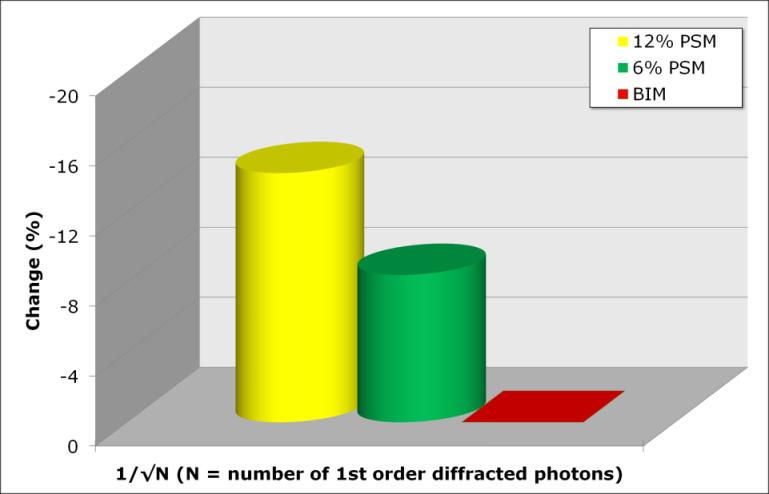
23 LWR & 1/ N (Cont.) LWR 1 N
24 What is photon shot noise? Attenuated PSM Stochastic simulation condition Simulation result Conclusion
25 Conclusion Phase shift mask concept has been proposed to mitigate photon shot noise effect With proposed PSM, simulation results showed - Higher relative intensity vs. BIM - Transfer more 1 st order diffracted photons onto wafer - Alleviate photon shot noise effect at even lower E op - lmproved LWR absorbed photons from 1 st order diffraction!! Confirmed that 1 st order diffracted photons are informative photons that affect photon shot noise effect Possibility of further works on PSM concept for even better performance!


26
Preliminary Investigation of Shot Noise, Dose, and Focus Latitude for E-Beam Direct Write
 Preliminary Investigation of Shot Noise, Dose, and Focus Latitude for E-Beam Direct Write Alan Brodie, Shinichi Kojima, Mark McCord, Luca Grella, Thomas Gubiotti, Chris Bevis KLA-Tencor, Milpitas, CA 94035
Stochastics and the Phenomenon of Line-Edge Roughness
 Stochastics and the Phenomenon of Line-Edge Roughness Chris Mack February 27, 2017 Tutorial talk at the SPIE Advanced Lithography Symposium, San Jose, California What s so Hard about Roughness? Roughness
Computational Lithography Turning Physics into Yield
 Computational Lithography Turning Physics into Yield Tim Fühner Fraunhofer IISB Erlangen, Germany SEMICON Europa, TechArena, 11.10.2012 Lithography Modeling 2 SEMICON Europa, TechArena, 11.10.2012 Computational
Reflectivity metrics for optimization of anti-reflection coatings on wafers with topography
 Reflectivity metrics for optimization of anti-reflection coatings on wafers with topography Mark D. Smith, Trey Graves, John Biafore, and Stewart Robertson KLA-Tencor Corp, 8834 N. Capital of Texas Hwy,
Optimization of Photolithography Process Using Simulation
 Optimization of Photolithography Process Using Simulation Introduction The progress in semiconductor technology towards even smaller device geometries demands continuous refinements of photolithography
Impact of mask line roughness in EUV lithography
 Impact of mask line roughness in EUV lithography Alessandro Vaglio Pret a,b, Roel Gronheid a, Trey Graves c, Mark D. Smith c, John Biafore c a IMEC, Kapeldreef 75, B-3001 Leuven, Belgium b Katholieke Universiteit
Using the Normalized Image Log-Slope, part 5: Development
 T h e L i t h o g r a p h y E x p e r t (February ) Using the Normalized Image Log-Slope, part 5: Development Chris A. Mack, KLA-Tencor, FINLE Division, Austin, Texas This recent series of Lithography
OPC flare and optical modeling requirements for EUV
 OPC flare and optical modeling requirements for EUV Lena Zavyalova, Kevin Lucas, Brian Ward*, Peter Brooker Synopsys, Inc., Austin, TX, USA 78746 *Synopsys assignee to IMEC, Leuven, Belgium B3001 1 Abstract
The Death of the Aerial Image
 Tutor50.doc: Version 5/9/05 T h e L i t h o g r a p h y E x p e r t (August 005) The Death of the Aerial Image Chris A. Mack, KLA-Tencor, FINLE Division, Austin, Texas The aerial image is, quite literally,
The impact of resist model on mask 3D simulation accuracy beyond. 40nm node memory patterns
 The impact of resist model on mask D simulation accuracy beyond nm node memory patterns Kao-Tun Chen a, Shin-Shing Yeh a, Ya-Hsuan Hsieh a, Jun-Cheng Nelson Lai a, Stewart A. Robertson b, John J. Biafore
Benefiting from Polarization: Effects at High-NA Imaging
 Benefiting from Polarization: Effects at High-NA Imaging Bruce W. Smith L. Zavyalova, A. Estroff, Y. Fan, A. Bourov Rochester Institute of Technology P. Zimmerman International SEMACH and Intel J. Cashmore
Photoresist Qualification using Scatterometry CD
 Photoresist Qualification using Scatterometry CD Roie Volkovich *a, Yosef Avrahamov a, Guy Cohen a, Patricia Fallon b, Wenyan Yin b, a KLA-Tencor Corporation Israel, Halavian St., P.O.Box 143, Migdal Haemek
Investigation of the foot-exposure impact in hyper-na immersion lithography when using thin anti-reflective coating
 Investigation of the foot-exposure impact in hyper-na immersion lithography when using thin anti-reflective coating Darron Jurajda b, Enrico Tenaglia a, Jonathan Jeauneau b, Danilo De Simone a, Zhimin
Defect Repair for EUVL Mask Blanks
 Defect Repair for EUVL Mask Blanks A.Barty, S.Hau-Riege, P.B.Mirkarimi, D.G.Stearns, H.Chapman, D.Sweeney Lawrence Livermore National Laboratory M.Clift Sandia National Laboratory E.Gullikson, M.Yi Lawrence
Investigation of interactions between metrology and lithography with a CD SEM simulator
 Investigation of interactions between metrology and lithography with a CD SEM simulator Mark D. Smith, Chao Fang, John J, Biafore, Alessandro Vaglio Pret, Stewart A. Robertson KLA-Tencor Corp. ABSTRACT
Design Rule Optimization of Regular layout for Leakage Reduction in Nanoscale Design
 Design Rule Optimization of Regular layout for Leakage Reduction in Nanoscale Design Anupama R. Subramaniam, Ritu Singhal, Chi-Chao Wang, Yu Cao Department of Electrical Engineering, Arizona State University,
EUV Lithography and Overlay Control
 YMS Magazine DECEMBER 2017 EUV Lithography and Overlay Control Efi Megged, Mark Wylie and Cathy Perry-Sullivan L A-Tencor Corporation One of the key parameters in IC fabrication is overlay the accuracy
Challenges in Manufacturing of optical and EUV Photomasks Martin Sczyrba
 Challenges in Manufacturing of optical and EUV Photomasks Martin Sczyrba Advanced Mask Technology Center Dresden, Germany Senior Member of Technical Staff Advanced Mask Technology Center Dresden Key Facts
Supreme lithographic performance by simple mask layout based on lithography and layout co-optimization
 Supreme lithographic performance by simple mask layout based on lithography and layout co-optimization Koichiro Tsujita a, Tadashi Arai a, Hiroyuki Ishii a, Yuichi Gyoda a, Kazuhiro Takahashi a, Valery
Iterative procedure for in-situ EUV optical testing with an incoherent source
 APS/123-QED Iterative procedure for in-situ EUV optical testing with an incoherent source Ryan Miyakawa and Patrick Naulleau Lawrence Berkeley National Laboratory, Berkeley, CA 94720 Avideh Zakhor Dept.
On the quality of measured optical aberration coefficients using phase wheel monitor
 On the quality of measured optical aberration coefficients using phase wheel monitor Lena V. Zavyalova *, Aaron R. Robinson, Anatoly Bourov, Neal V. Lafferty, and Bruce W. Smith Center for Nanolithography
Three-dimensional imaging of 30-nm nanospheres using immersion interferometric lithography
 Three-dimensional imaging of 30-nm nanospheres using immersion interferometric lithography Jianming Zhou *, Yongfa Fan, Bruce W. Smith Microelectronics Engineering Department, Rochester Institute of Technology,
CSPLAT for Photolithography Simulation
 CSPLAT for Photolithography Simulation Guoxiong Wang wanggx@vlsi.zju.edu.cn Institute of VLSI Design, Zhejiang University 2001.8.31 Outline Photolithographic system Resolution enhancement technologies
Benefiting from polarization effects on high-na imaging
 Benefiting from polarization effects on high-na imaging Bruce W. Smith, Lena Zavyalova, Andrew Estroff Rochester Institute of Technology, Microelectronic Engineering Department 82 Lomb Memorial Drive,
Characterization of a Chemically Amplified Photoresist for Simulation using a Modified Poor Man s DRM Methodology
 Characterization of a Chemically Amplified Photoresist for Simulation using a Modified Poor Man s DRM Methodology Nickhil Jakatdar 1, Xinhui Niu, Costas J. Spanos Dept. of Electrical Engineering and Computer
Image Degradation due to Phase Effects in Chromeless Phase Lithography
 Image Degradation due to Phase Effects in Chromeless Phase Lithography Karsten Bubke *, Martin Sczyrba, KT Park, Ralf Neubauer, Rainer Pforr 2, Jens Reichelt 2, Ralf Ziebold 2 Advanced Mask Technology
Copyright 2002 by the Society of Photo-Optical Instrumentation Engineers.
 Copyright by the Society of Photo-Optical Instrumentation Engineers. This paper was published in the proceedings of Optical Microlithography XV, SPIE Vol. 469, pp. 5-37. It is made available as an electronic
Mask patterning challenges for EUV N7 and beyond. Date: 2018/02/27
 Mask patterning challenges for EUV N7 and beyond Date: 2018/02/27 Outline EUV tech drivers and mask roadmap N7 mask process status Mask and mask process characterization Process improvements toward N5
SMO Photomask Inspection in the Lithographic Plane
 SMO Photomask Inspection in the Lithographic Plane Emily Gallagher 1, Karen Badger 1, Yutaka Kodera 2, Jaione Tirapu Azpiroz 3, Ioana Graur 3 Scott D. Halle 4, Kafai Lai 3, Gregory R. McIntyre 4, Mark
Outline. Abstract. Modeling Approach
 EUV Interference Lithography Michael Goldstein ϕ, Donald Barnhart λ, Ranju D. Venables ϕ, Bernice Van Der Meer ϕ, Yashesh A. Shroff ϕ ϕ = Intel Corporation (www.intel.com), λ = Optica Software (www.opticasoftware.com)
EUV telecentricity and shadowing errors impact on process margins
 EUV telecentricity and shadowing errors impact on process margins D. Civay 1*, E. Hosler 1, V. Chauhan 1, T. Guha Neogi 1, L. Smith 1, D. Pritchard 1 1 GLOBALFOUNDRIES, Malta, NY, USA ABSTRACT Monte Carlo
Photoresist Modulation Curves
 Photoresist Modulation Curves Anatoly Bourov, Yongfa Fan, Frank C. Cropanese, Bruce W. Smith Rochester nstitute of Technology, 82 Lomb Memorial Dr., Rochester, NY 14623 ABSTRACT Photoresist modulation
Materials for and performance of multilayer lithography schemes
 Materials for and performance of multilayer lithography schemes Marc Weimer, Yubao Wang, Charles J. Neef, James Claypool, Kevin Edwards, Zhimin Zhu Brewer Science, Inc., 2401 Brewer Dr., Rolla, MO, USA
SuMMIT Application Notes:
 SuMMIT Application Notes: #2 Tools for large data sets EUV Technology, SuMMIT Software Division Large data sets support high precision SuMMIT allows for batch processing of large data sets for such studies
Maaike Op de Beeck, Erik Sleeckx, Patrick Jaenen, Eddy Kunnen, IMEC Leuven, Belgium Wendy Yeh, Applied Materials Santa Clara, CA
 EXCLUSIVE ONLINE FEATURE Immersion lithography using a dual-function BARC Maaike Op de Beeck, Erik Sleeckx, Patrick Jaenen, Eddy Kunnen, IMEC Leuven, Belgium Wendy Yeh, Applied Materials Santa Clara, CA
Frontiers in CD-SEM metrology
 Frontiers in CD-SEM metrology abeam Technologies, Inc. Dr. Sergey Babin, sb@abeamtech.com Hayward, CA, USA CD-SEM in semiconductor CD-SEM is an indispensable part of the semiconductor industry In volume
Immersion Microlithography at 193 nm with a Talbot Prism Interferometer
 RIT Scholar Works Presentations and other scholarship 5-28-2004 Immersion Microlithography at 193 nm with a Talbot Prism Interferometer Anatoly Bourov Yongfa Fan Frank Cropanese Neal Lafferty Lena V. Zavyalova
ABSTRACT. KEYWORDS: AIMS, Bossung plot, linewidth versus defocus, quartz height, EAPSM, repair verification, MeRiT, Litho simulation INTRODUCTION
 A novel method for utilizing AIMS to evaluate mask repair and quantify over-repair or under-repair condition Doug Uzzel 1, Anthony Garetto 2, Krister Magnusson 2, Gilles Tabbone 2 1 Photronics, Inc., 10136
Direct Imaging Solutions for Advanced Fan-Out Wafer-Level and Panel-Level Packaging
 Semicon Europe 2018 Direct Imaging Solutions for Advanced Fan-Out Wafer-Level and Panel-Level Packaging November 16, 2018 by Mark Goeke SCREEN SPE Germany GmbH 1 SCREEN Semiconductor s Target Market Target
Manufacturability of computation lithography mask: Current limit and requirements for sub-20nm node
 Manufacturability of computation lithography mask: Current limit and requirements for sub-20nm node Jin Choi, In-Yong Kang, Ji Soong Park, In Kyun Shin, and Chan-Uk Jeon Samsung Electronics Co., Ltd, San
Practical approach to full-field wavefront aberration measurement using phase wheel targets
 Practical approach to full-field wavefront aberration measurement using phase wheel targets Lena V. Zavyalova *a, Bruce W. Smith a, Anatoly Bourov a, Gary Zhang b, Venugopal Vellanki c, Patrick Reynolds
Applications of DSA for lithography
 Applications of DSA for lithography Yoshi Hishiro, Takehiko Naruoka, JSR Micro Inc. Yuusuke Anno JSR Micro NV. Hayato Namai, Fumihiro Toyokawa, Shinya Minegishi, Yuuji Namie, Tomoki Nagai, Kentaro Goto,
Rigorous electromagnetic simulation of mask magnification effects on the diffracted light for EUV binary mask
 Microelectronic Engineering 84 (2007) 711 715 www.elsevier.com/locate/mee Rigorous electromagnetic simulation of mask magnification effects on the diffracted light for EUV binary mask Chun-Hung Lin a,
Measurement and characterization of EUV mask performance at high-na
 Measurement and characterization of EUV mask performance at high-na Rikon Chao Andrew R. Neureuther, Ed. Laura Waller, Ed. Patrick Naulleau, Ed. Electrical Engineering and Computer Sciences University
Strengthening the leadership
 Strengthening the leadership Press conference, SEMICON West 2005 Martin van den Brink, Executive Vice President ASML / Slide 1 Safe Harbor Safe Harbor Statement under the U.S. Private Securities Litigation
Sub-wavelength Holographic Lithography: The Possibilities And Advantages. (NANOTECH SWHL, 6-1 Kazarmenny per., Moscow, Russia)
") Sub-wavelength Holographic Lithography: The Possibilities And Advantages Mikhail V. Borisov, Dmitriy A. Chelyubeev, Vitalij V. Chernik, Alexander A. Gavrikov, Dmitriy Yu. Knyazkov, Petr A. Mikheev, Vadim
Sub-wavelength Holographic Lithography: The Possibilities And Advantages Mikhail V. Borisov, Dmitriy A. Chelyubeev, Vitalij V. Chernik, Alexander A. Gavrikov, Dmitriy Yu. Knyazkov, Petr A. Mikheev, Vadim
Analytic Derivation and Minimization of Line Edge Roughness in Electron-beam Lithography. Rui Guo
 Analytic Derivation and Minimization of Line Edge Roughness in Electron-beam Lithography by Rui Guo A dissertation submitted to the Graduate Faculty of Auburn University in partial fulfillment of the requirements
New methodology to characterize printing performance of mask materials by analyzing diffraction efficiency
 9-Oct-7 4th nternational Symposium on mmersion Lithography * The title has been modified [ 865 ; P-HM-5/5 ] New methodology to characterize printing performance of mask materials by analyzing diffraction
Optical Lithography Modelling with MATLAB
 Optical Lithography Modelling with MATLAB 2 Laboratory Manual to accompany Fundamental Principles of Optical Lithography, by Chris Mack 2 Optical Lithography Modelling with MATLAB Kevin Berwick Optical
SIMULATION FOR ADVANCED MASK ALIGNER LITHOGRAPHY
 SIMULATION FOR ADVANCED MASK ALIGNER LITHOGRAPHY Ulrich Hofmann, Daniel Ritter, Balint Meliorisz, Nezih Unal GenISys GmbH Germany Dr. Michael Hornung, Ralph Zoberbier SUSS MicroTec Lithography GmbH Germany
Dynamic Performance of DUV Step & Scan Systems and Process Latitude
 Dynamic Performance of DUV Step & Scan Systems and Process Latitude Michel Klaassen, Marian Reuhman, Antoine Loock Mike Rademaker, Jack Gemen ASML, De Run 111, 553 LA Veldhoven, The Netherlands This paper
Overlay control methodology comparison: field-by-field and high-order methods
 Overlay control methodology comparison: field-by-field and high-order methods Chun-Yen Huang a, Chui-Fu Chiu a, Wen-Bin Wu a, Chiang-Lin Shih a, Chin-Chou Kevin Huang* b, Healthy Huang c, DongSub Choi
Advanced Simulation Techniques for Thick Photoresist Lithography
 SPIE 1997 349-72 Advanced Simulation Techniques for Thick Photoresist Lithography Warren W. Flack, Gary Newman Ultratech Stepper, Inc. San Jose, CA 95134 D. Bernard, J. Rey, Y. Granik, V. Boksha Technology
Low k 1 Logic Design using Gridded Design Rules
 SPIE Advanced Lithography Conference 2008 6925-68 Tela Innovations, ASML 1 Low k 1 Logic Design using Gridded Design Rules Michael C. Smayling a, Hua-yu Liu b, Lynn Cai b a Tela Innovations, Inc., 655
Extreme Ultraviolet Phase Contrast Imaging
 Extreme Ultraviolet Phase Contrast Imaging Gregory Denbeaux 1, Rashi Garg 1, Andy Aquila 2, Anton Barty 3, Kenneth Goldberg 2, Eric Gullikson 2, Yanwei Liu 2, Obert Wood 4 1, University at Albany, Albany,
Study of Air Bubble Induced Light Scattering Effect On Image Quality in 193 nm Immersion Lithography
 Study of Air Bubble Induced Light Scattering Effect On Image Quality in 193 nm Immersion Lithography Y. Fan, N. Lafferty, A. Bourov, L. Zavyalova, B. W. Smith Rochester Institute of Technology Microelectronic
Overlay accuracy fundamentals
 accuracy fundamentals Daniel Kandel Vladimir Levinski Noam Sapiens Guy Cohen Eran Amit Dana Klein Irina Vakshtein KLA-Tencor Corporation 1 Halavyan Street Migdal Haemek 31 Israel ABSTRACT Currently the
A New Fast Resist Model: the Gaussian LPM
 A New Fast Resist Model: the Gaussian LPM Chris A. Mack Lithoguru.com, 65 Watchhill Rd, Austin, TX 7873 Abstract BACKGROUN: Resist models for full-chip lithography simulation demand a difficult compromise
Waves & Oscillations
 Physics 42200 Waves & Oscillations Lecture 37 Interference Spring 2016 Semester Matthew Jones Multiple Beam Interference In many situations, a coherent beam can interfere with itself multiple times Consider
A novel methodology for Litho-to-Etch Pattern Fidelity Correction for SADP Process
 A novel methodology for Litho-to-Etch Pattern Fidelity Correction for SADP Process Shr-Jia Chen* a, Yu-Cheng Chang a, Arthur Lin b, Yi-Shiang Chang a, Chia-Chi Lin a, Jun-Cheng Lai a a Powerchip Technology
SUSS MJB4. Manual Aligner For Research, Development and Operator Assisted Production October, 2009
 SUSS MJB4 Manual Aligner For Research, Development and Operator Assisted Production October, 2009 Overview Product Portfolio Aligner MA/BA 8 MA200Compact LithoFab200 MJB4 MA300Plus MA/BA 6 MA150e LithoPack300
Snell or Fresnel The influence of material index on hyper NA lithography
 Snell or Fresnel The influence of material index on hyper NA lithography Bruce Smith and Jianming Zhou Rochester Institute of Technology, Center for Nanolithography Research Microelectronic Engineering
Analysis of an Effect of Perturbations in SWHM and Illuminating Optical Scheme Parameters on an Aerial Image
 Analysis of an Effect of Perturbations in SWHM and Illuminating Optical Scheme Parameters on an Aerial Image Borisov M.V., Chelyubeev D.A., Chernik V.V., Gavrikov A.A., Knyazkov D.Yu., Mikheev P.A., Rakhovskіy
Hybrid hotspot detection using regression model and lithography simulation
 Hybrid hotspot detection using regression model and lithography simulation Taiki Kimura 1a, Tetsuaki Matsunawa a, Shigeki Nojima a and David Z. Pan b a Toshiba Corp. Semiconductor & Storage Products Company,
Model-Based MPC Enables Curvilinear ILT using Either VSB or Multi-Beam Mask Writers
 Model-Based MPC Enables Curvilinear ILT using Either VSB or Multi-Beam Mask Writers Leo (Linyong) Pang, Yutesu Takatsukasa, Daisuke Hara, Michael Pomerantsev, Bo Su, Aki Fujimura D2S Patented Technology
PRODUCT OVERVIEW. Rupert Perera President, EUV Tech
 PRODUCT OVERVIEW Rupert Perera President, EUV Tech EUV TECH OVERVIEW Started in 1997, EUV Tech has pioneered the development of EUV metrology tools: EUV Reflectometer o Measures the reflectivity and uniformity
Fast Lithography Simulation under Focus Variations for OPC and Layout Optimizations
 Fast Lithography Simulation under Focus Variations for OPC and Layout Optimizations Peng Yu a, David Z. Pan a and Chris A. Mack a,b a Electrical and Computer Engineering Department, University of Texas
Job Deck and Schedule File Instructions
 Job Deck and Schedule File Instructions The instructions which determine how your pattern is applied to a wafer or other writing substrate, is determined by two files; the Job Deck file (.jdf) and the
Multi-Level Overlay Techniques for Improving DPL Overlay Control
 Multi-Level Overlay Techniques for Improving DPL Overlay Control Charlie Chen 1, C Pai, Dennis u 1, Peter Pang 1, Chun Chi u 1, Robert (Hsing-Chien) Wu, Eros (Chien Jen) Huang, Marson (Chiun-Chieh) Chen,
Lithography Simulation
 Stepper Laser Proximity e-beam Lithography Simulation Enable next generation products and faster development by computational design and process optimization www.genisys-gmbh.com Source Condenser Mask
Chapter 24. Wave Optics
 Chapter 24 Wave Optics Wave Optics The wave nature of light is needed to explain various phenomena Interference Diffraction Polarization The particle nature of light was the basis for ray (geometric) optics
FOURIER-TRANSFORM INTERFERENCE LITHOGRAPHY
 FOURIER-TRANSFORM INTERFERENCE LITHOGRAPHY M. BULINSKI 1, G. MOAGÃR-POLADIAN 2* 1 Faculty of Physics, Bucharest University, str. Atomiştilor nr. 405, Bucureşti-Măgurele, România, E- 2 National Institute
Coupling of surface roughness to the performance of computer-generated holograms
 Coupling of surface roughness to the performance of computer-generated holograms Ping Zhou* and Jim Burge College of Optical Sciences, University of Arizona, Tucson, Arizona 85721, USA *Corresponding author:
Optimal frequency coverages and parsings for imaging interferometric lithography
 J. Microlith., Microfab., Microsyst. 4 3, 033005 Jul Sep 2005 Optimal frequency coverages and parsings for imaging interferometric lithography Thanis M. Tridhavee University of New Mexico Department of
Computer Vision. The image formation process
 Computer Vision The image formation process Filippo Bergamasco (filippo.bergamasco@unive.it) http://www.dais.unive.it/~bergamasco DAIS, Ca Foscari University of Venice Academic year 2016/2017 The image
Manufacturing Challenges and their Implications on Design
 Manufacturing Challenges and their Implications on Design Phiroze Parakh, Ph.D 45nm/32nm Design Challenges MANUFACTURING VARIATIONS PROCESS & DESIGN VARIATIONS LARGE DESIGNS LOW POWER The Evolution of
3D Holographic Lithography
 3D Holographic Lithography Luke Seed, Gavin Williams, Jesus Toriz-Garcia Department of Electronic and Electrical Engineering University of Sheffield Richard McWilliam, Alan Purvis, Richard Curry School
Amherst. University of Massachusetts Amherst. Aswin Sreedhar University of Massachusetts Amherst
 University of Massachusetts Amherst ScholarWorks@UMass Amherst Masters Theses 1911 - February 2014 2008 Automatic Techniques for Modeling Impact of Sub-wavelength Lithography on Transistors and Interconnects
CSE 681 Illumination and Phong Shading
 CSE 681 Illumination and Phong Shading Physics tells us What is Light? We don t see objects, we see light reflected off of objects Light is a particle and a wave The frequency of light What is Color? Our
High Throughput Maskless Lithography
 High Throughput Maskless Lithography Sokudo lithography breakfast forum July 14 th 2010 Bert Jan Kampherbeek, VP Market Development and co-founder Agenda MAPPER s Objective MAPPER s Status MAPPER s Roadmap
PTFE Reflectance Measurements, Modeling and Simulation for Xenon Detectors
 PTFE Reflectance Measurements, Modeling and Simulation for Xenon Detectors Claudio F. P. Silva University of Coimbra LIP Laboratory Chicago, 11 June 2011 TIPP 2011 PTFE reflectance measurements, modeling
Pushing 193i lithography by Joint optimization of Layout and Lithography
 Pushing 193i lithography by Joint optimization of Layout and Lithography Peter De Bisschop Imec, Leuven, Belgium Semicon Europe Messe Dresden, Germany Lithography session October 12, 2011 Semiconductor-Industry
WAVELENGTH MANAGEMENT
 BEAM DIAGNOS TICS SPECIAL PRODUCTS OEM DETECTORS THZ DETECTORS PHOTO DETECTORS HIGH POWER SOLUTIONS POWER DETECTORS ENERGY DETECTORS MONITORS Camera Accessories WAVELENGTH MANAGEMENT UV CONVERTERS UV Converters
Basic Polarization Techniques and Devices 1998, 2003 Meadowlark Optics, Inc
 Basic Polarization Techniques and Devices 1998, 2003 Meadowlark Optics, Inc This application note briefly describes polarized light, retardation and a few of the tools used to manipulate the polarization
Local Reflection Models
 Local Reflection Models Illumination Thus Far Simple Illumination Models Ambient + Diffuse + Attenuation + Specular Additions Texture, Shadows, Used in global algs! (Ray tracing) Problem: Different materials
ILT for Double Exposure Lithography with Conventional and Novel Materials
 ILT for Double Exposure Lithography with Conventional and Novel Materials Amyn Poonawala a and Yan Borodovsky b and Peyman Milanfar c a Department of Computer Engineering, University of California, Santa
Current status and expectation of EUV lithography
 2014 International Workshop on EUV Lithography Current status and expectation of EUV lithography June 26, 2014 Takayuki UCHIYAMA TOSHIBA Corporation Copyright 2014, Toshiba Corporation. Contents Introduction
Announcements. Advanced Digital Integrated Circuits. No office hour next Monday. Lecture 2: Scaling Trends
 EE24 - Spring 2008 Advanced Digital Integrated Circuits Lecture 2: Scaling Trends Announcements No office hour next Monday Extra office hours Tuesday and Thursday 2-3pm 2 CMOS Scaling Rules Voltage, V
Sub-Wavelength Holographic Lithography SWHL. NANOTECH SWHL Prof. Dr. Vadim Rakhovsky October, 2012
 Sub-Wavelength Holographic Lithography SWHL NANOTECH SWHL Prof. Dr. Vadim Rakhovsky October, 2012 EXECUTIVE SUMMARY SWHL is a new, alternative low cost approach to lithography SWHL is suitable for all
Process Variation Aware OPC with Variational Lithography Modeling
 Process Variation Aware OPC with Variational Lithography Modeling Peng Yu ECE Department University of Texas at Austin Austin, TX 78712 yupeng@cerc.utexas.edu Sean X. Shi ECE Department University of Texas
Supplementary Figure 1 Optimum transmissive mask design for shaping an incident light to a desired
 Supplementary Figure 1 Optimum transmissive mask design for shaping an incident light to a desired tangential form. (a) The light from the sources and scatterers in the half space (1) passes through the
Physical or wave optics
 Physical or wave optics In the last chapter, we have been studying geometric optics u light moves in straight lines u can summarize everything by indicating direction of light using a ray u light behaves
Modeling of Mask Thermal Distortion during Optical Lithography and Its Dependence on Pattern Density Distribution
 Modeling of Mask Thermal Distortion during Optical Lithography and Its Dependence on Pattern Density Distribution M.S. Thesis Qiaolin Zhang Department of Electrical Engineering and Computer Science University
Analysis of OPC Features in Binary Masks at 193nm
 Analysis of OPC Features in Binary Masks at 193nm Konstantinos Adam, Andrew R. Neureuther EECS Department, University of California at Berkeley Berkeley, CA 94720 email: kadam@eecs.berkeley.edu, neureuth@eecs.berkeley.edu
Defocus based phase imaging for quantifying electromagnetic edge effects in photomasks
 Defocus based phase imaging for quantifying electromagnetic edge effects in photomasks Aamod Shanker Laura Waller, Ed. Andrew R. Neureuther, Ed. Electrical Engineering and Computer Sciences University
Fabrication of the photo-resist mask onto 3D nonplanar wafer for micro abrasive jet machining
 Fabrication of the photo-resist mask onto 3D nonplanar wafer for micro abrasive jet machining 1 J. B. Byiringiro, 1a T. J. Ko, 2 H.C. Kim, 3 I.H. Lee Abstract This paper presents a novel fabrication technique
specular diffuse reflection.
 Lesson 8 Light and Optics The Nature of Light Properties of Light: Reflection Refraction Interference Diffraction Polarization Dispersion and Prisms Total Internal Reflection Huygens s Principle The Nature
Chapter 37. Wave Optics
 Chapter 37 Wave Optics Wave Optics Wave optics is a study concerned with phenomena that cannot be adequately explained by geometric (ray) optics. Sometimes called physical optics These phenomena include:
SYDE 575: Introduction to Image Processing
 SYDE 575: Introduction to Image Processing Image Enhancement and Restoration in Spatial Domain Chapter 3 Spatial Filtering Recall 2D discrete convolution g[m, n] = f [ m, n] h[ m, n] = f [i, j ] h[ m i,
Coping with Variability in Semiconductor Manufacturing
 1 Coping with Variability in Semiconductor Manufacturing Costas J. Spanos Berkeley Computer Aided Manufacturing Department of EECS University of California, Berkeley 12/6/04 2 The Traditional Semiconductor