Applications of DSA for lithography
|
|
|
- Jocelin McCoy
- 5 years ago
- Views:
Transcription

1 Applications of DSA for lithography Yoshi Hishiro, Takehiko Naruoka, JSR Micro Inc. Yuusuke Anno JSR Micro NV. Hayato Namai, Fumihiro Toyokawa, Shinya Minegishi, Yuuji Namie, Tomoki Nagai, Kentaro Goto, Masayuki Motonari, Yoshikazu Yamaguchi JSR Corp.

2 Lithography Roadmap DSA has been the candidate for next generation lithography since DSA appeared on ITRS lithography roadmap from DSA attracts increasing attention because of the delay of EUV development. 2

3 Block Copolymers VS Polymer Blends Block copolymer Polymer blend 1. Phase-separated polymer domains Intrinsic dimension and pre-determined morphology No specific dimension, morphology, or periodicity DSA DSA 2. Phase separation in pre-pattern 3. Material/Process flexibility Pitch multiplication Block copolymer keeps intrinsic periodicity and morphology Specialty polymers High bake temperature (-250C) Difficult to perform wet development Need ultra-high molecular weight to achieve large features Sidewall image transfer Morphology and dimension are determined by pre-pattern and blend composition Huge material selection Low bake temperature (-120C) Wet- or Dry-etching can be applied to selectively remove one component Can apply to large dimensions This paper will focus mainly on DSA process using polymer blend but touch on Bolck copolymer system also. 3
4 Sidewall Image Transfer with Phase Separation of Si Containing Polymer Blend 1st Patterning Basic Process Flow Pre-pattern Polymer blend coating SOC/BARC Baking 100~140C/60s Silicon polymer Organic polymer Etching (Wet or dry) Pattern transfer Annealing 4

=2.")
 LWR(3 )=3.")
5 Polymer Blend DSA for 22nm HP Spacers SPIE co-work of JSR&IBM Polymer blend coating Baking Silicon polymer Organic polymer Etching (Wet or dry) 26nmL88nmP CD=26.3 nm LER=2.8 nm LWR=4.8nm CD=19.2nm LER(3 )=2.9nm (Pre-pattern side) LER(3 )=3.3nm (Organic polymer side) LWR(3 )=3.5nm Application of polymer blend DSA for LS patterning was demonstrated. 5

6 Applications of polymer blends DSA for CH application CH shrink application 1 Polymer blend coating Silicon Polymer Silicon Polymer CH repair by DSA shrink Organic polymer Silicon Polymer DSA Pattern Doubling process Resist DSA Resist Resist Silicon Polymer Silicon polymer 1. DSA shrink process with block copolymer was reported by IBM. J. Cheng et al SPIE
7 CH Shrink Application Guide-pattern Si polymer Organic polymer Polymer blend coating SiARC Organic Hard Mask Silicon polymer Annealing ( C/60s-90s) Organic polymer Remove Organic Polymer (wet developmant) Simple process (low DSA bake temperature, existing SiARC) could be applied in polymer blend DSA shrink process. Shrink process with Block Copolymer J. Cheng et al SPIE Guide-pattern Annealing BCP coating (>200C) Dry etch Neutral Layer 7

")
 After")


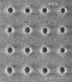
8 Results of CH Shrink Application (Top-Down) Guide-pattern (110nmP) After DSA shrink 55.6nm 33.2nm 100K 100K 70K 70K Over 20nm shrink amounts was observed in DSA shrink process. 8

; 4.")
: 4.0nm Max CD: 32.1nm Min CD: 25.7nm CD(nm) 30.5-31.5 29.5-30.5 28.5-29.5 27.5-28.5 26.5-27.5 25.5-26.5 24.5-25.5 23.5-24.5 22.5-23.")
9 DSA material; JSR DS003X Bake; 120C/90s Full-Field CDU Evaluation Guide Pattern: 55nmH110nmP After DSA Shrink DS003X # # # # # # # # # # # # # # # # # # # # # # # # # # # # # # # # # # # # # # # # # # # # # # # # # # # # # # # # # # # # # # # # # # # # # # # # # # # # # # # # # # # # # # # # # # # # # # # # # # # # # # # # # # # # # # # # # # # # # # # # # # # # # # # # # # # # # # # # # # # # # # # # # # # # # # # # # # # # # # # # # # # # # # # # # # # # # # # # # # # # # # # # # # # # # # # # # # # # # # # # # # # # # # # # # # # # # # # # # # # # # # # # # # # # # # # # # # # # # # # # # # # # # # # # # # # # # # # # # # # # # # # # # # # # # # # # # # # # # # # # # # # # # # # # # # # # # # # # # # # # # # # # # # # # # # # # # # # # # # # # # # # # # # # # # # # # # # # # # # # # # # # # # # # # # # # # # # # # # # # # # # # # # # # # # # # # # # # # # # # # # # # # # # # # # # # # # # # # # # # # # # # # # # # # # # # # # # # # # # # # # # # # # # # # # # # # # # # # # # # # # # # # # # # # # # # # # # # # # # # # # # # # # # # # # # # # # # # # # # # # # # # # # # # # # # # # # # # # # # # # # ### ### # # # # # # # # # # # # # # # # # # # # # # # # # # # # # # # # # # # # # # # # # # # # # # # # # # # # # # # # # # # # # # # # # # # # # # # # # # # # # # # # # # # # # # # # # # # # # # # # # # # # # # # # # # # # # # # # # # # # # # # # # # # # # # # # # # # # # # # # # # # # # # # # # # # # # # # # # # # # # # # # # # # # # # # # # # # # # # # # # # # # # # # # # # # # # # # # # # # # # # # # # # # # # # # # # # # # # # # # # ### # # # # # # # # # # # # # # # # # # # # # # # # # # # # # # # # # # # # # # # # # # # # # # # # # # # # # # # # # # # # # # # # # # # # # # # # # # # # # # # # # # # # # # # # # # # # # # # # # # # # # # # # # # # # # # # # # # # # # # # # # # # # # # # #### # # # # # # # # # # # # # # # # # # # # # # # # # # # # # # # # # # # # # # # # # ### # # # # # # # # # # # # # # # # # # # # # # # # # # # # # # # # # # # 3 (local); 4.6nm 3 (local); 4.0nm Avg.CD: 55.8nm 3 (in wafer): 4.9nm Max CD: 59.5nm Min CD: 50.7nm CD(nm) Avg.CD: 28.6nm 3 (in wafer): 4.0nm Max CD: 32.1nm Min CD: 25.7nm CD(nm) CDU improvement in DSA shrink process was observed. 9
10 CH Repair by DSA Shrink Concept Silicon-Organic Blend Polymer Si polymer Organic polymer Silicon Polymer Organic Polymer Polymer blend coating DSA Annealing Remove Organic layer Diamond shape Normal Hole Hole Repair by DSA shrink 10


 Hole profile")
11 CH Repair by DSA Shrink (1) 71.9nmH110nmP 43.4nmH110nmP DSA Organic polymer removal 100K 100K Before Shrink After Shrink Silicon Polymer Profile Repair (Circularity improvement) Hole profile was effectively repaired by DSA shrink process. 11


12 CH Repair by DSA Shrink 120nmP 63.1nmH120nmP DSA Organic polymer removal 100K 100K Before Shrink After Shrink Silicon Polymer Profile Repair (CH Reassembly) Hole profile was effectively repaired by DSA shrink process. 12


13 Blend DSA Shrink and Repair for Various Patterns Blend DSA reduce hole size with maintaining the shape of guide pattern. Blend DSA also work for pattern repair as well as size shrink. Elongated CH Shrink Pattern-A X=230.7nm Y=51.1nm L-plate trench Pattern-B X=51.4nm Y=296.6nm A:X/Y=4.5, B:Y/X=5.8 Pattern-A X=179.9nm Y=41.5nm Pattern-B X=40.9nm Y=234.6nm A:X/Y=4.4, B:Y/X=5.7 Oval hole repair 200nm 200nm 13
14 Pattern Doubling Process by DSA shrink Concept Si polymer Organic polymer Polymer blend coating Organic Polymer Annealing (120C/90s) Resist Pillar Guide-pattern Silicon polymer Organic polymer removal Resist Resist Removal Silicon polymer Staggered Hole Pattern Grid Hole Pattern Silicon polymer 14


15 Guide-pattern Pillar guide-pattern:110nmp Pattern Doubling Demonstration by DSA Step.1 Grid: 55nmH110nmP Step.2 Staggered: 55nmH78nmP 100K 100K 100K Resist Pillar Resist Pillar Organic polymer Removal Resist Pillar Resist Removal X Y S Hole Staggered CD: 55nm X: 110nm Y: 110nm S: 78nm Organic Polymer Silicon Polymer Hole Silicon Polymer Hole Silicon Polymer Pattern doubling by polymer blend DSA was demonstrated. 15
16 CH Shrink by Block-co-Polymer
 PMMA")
17 CH Shrink by PS-b-PMMA 80nmCH was shrunk to CD=20nm hole with PS-b-PMMA. PMMA. Metal contents of DSA solution: less than 2ppb. Li, Na, Mg, Al, K,, Ca, C Ti, Cr, Mn, Fe, Ni, Cu, Zn, Zr, Pb Resist NL SiARC Organic Hard Mask Polymer Coating /Annealing (250C/300s) PMMA development
18 Beyond PS-b-PMMA


19 High Materials for Fine Patterning 8.4nm line pattern was formed with high block-co co-polymer BCP at 220C60s anneal under air. Guide resist BCP pattern L 0 =16.75nm 100nm Anneal condition Bake: 220C60s Atmosphere: Air
20 Summary Blend DSA was applied for sidewall L/S pitch splitting, hole pattern shrink, hole pattern repair, and hole pattern doubling process. EUV + DSA was examined to prove DSA can support EUV. BCP DSA is also used for CH shrink. Post PS-b-PMMA PMMA material was developed to form 8.4nmLS pattern.
21 Acknowledgment The authors gratefully thank to IBM Almaden Research stuff for valuable discussions and suggestions, especially for Joy Y. Cheng, Daniel P. Sanders, and Robert Allen. Thank you for kind attention! 21


22 We will develop materials for expansion of industry Thank you for your attention.
Further Optimization of SMART TM DSA Material and Process
 Further Optimization of SMART TM DSA Material and Process G. Lin, H. Wu, J. Kim, J. Yin, Y. Cao, J. Shan, Y. Her, S. Miyazaki, D. Baskaran and T. Tsutsumi Schematics of the SMART TM DSA process* NLD-175
DSA: How far have we come and how much further is left to go? Darron Jurajda
 DSA: How far have we come and how much further is left to go? Darron Jurajda Semiconductor Business Unit Director, Brewer Science Outline Background of DSA at Brewer Science DSA historical progress Hype
Approaches to the Metrology Challenges for DSA Hole
 Approaches to the Metrology Challenges for DSA Hole Masafumi Asano, Kazuto Matsuki, Tomoko Ojima, Hiroki Yonemitsu, Ayako Kawanishi, Miwa Sato 2015 Toshiba Corporation Introduction Outline Metrology for
New plasma processes for improved dimensional control and LWR for a 28nm gate patterning
 New plasma processes for improved dimensional control and LWR for a 28nm gate patterning Onintza Ros a, Erwine Pargon b, Sebatien Barnola c, Pascal Gouraud a, Marc Fouchier b a STMicroelectronics, 85 rue
Preliminary Investigation of Shot Noise, Dose, and Focus Latitude for E-Beam Direct Write
 Preliminary Investigation of Shot Noise, Dose, and Focus Latitude for E-Beam Direct Write Alan Brodie, Shinichi Kojima, Mark McCord, Luca Grella, Thomas Gubiotti, Chris Bevis KLA-Tencor, Milpitas, CA 94035
Advanced multi-patterning and hybrid lithography techniques. Fedor G Pikus, J. Andres Torres
 Advanced multi-patterning and hybrid lithography techniques Fedor G Pikus, J. Andres Torres Outline Need for advanced patterning technologies Multipatterning (MP) technologies What is multipatterning?
Pushing 193i lithography by Joint optimization of Layout and Lithography
 Pushing 193i lithography by Joint optimization of Layout and Lithography Peter De Bisschop Imec, Leuven, Belgium Semicon Europe Messe Dresden, Germany Lithography session October 12, 2011 Semiconductor-Industry
2013 International Workshop on EUV Lithography Hanyang University
 Agenda What is photon shot noise? Attenuated PSM Stochastic simulation condition Simulation result Conclusion What is photon shot noise? Attenuated PSM Stochastic simulation condition Simulation result
Mask patterning challenges for EUV N7 and beyond. Date: 2018/02/27
 Mask patterning challenges for EUV N7 and beyond Date: 2018/02/27 Outline EUV tech drivers and mask roadmap N7 mask process status Mask and mask process characterization Process improvements toward N5
OPC flare and optical modeling requirements for EUV
 OPC flare and optical modeling requirements for EUV Lena Zavyalova, Kevin Lucas, Brian Ward*, Peter Brooker Synopsys, Inc., Austin, TX, USA 78746 *Synopsys assignee to IMEC, Leuven, Belgium B3001 1 Abstract
CMOS TECHNOLOGY- Chapter 2 in the Text
 CMOS TECHOLOGY- Chapter 2 in the Text CMOS Technology- Chapter 2 We will describe a modern CMOS process flow. In the simplest CMOS technologies, we need to realize simply MOS and MOS transistors for circuits
Quality of Semiconductor Raw Materials: Evolution and Challenges. Yongqiang Lu Kevin McLaughlin
 Quality of Semiconductor Raw Materials: Evolution and Challenges Yongqiang Lu Kevin McLaughlin Outline Advance of Fab technologies and the evolution of raw materials for ever higher quality Challenges:
Directed Self-Assembly for the Semiconductor Industry
 Directed Self-Assembly for the Semiconductor Industry H.-S. Philip Wong, Chris Bencher # Linda He Yi, Xin-Yu Bao, Li-Wen Chang Stanford University, # Applied Materials Stanford University J.W. Jeong...C.A.
Olivier Vatel. Accelerated innovation through strategic collaboration: a view from an equipment supplier CTO. July 10, 2018 SE L1
 1 SE-77-3018-L1 SCREEN Semiconductor Solutions Co., Ltd. Accelerated innovation through strategic collaboration: a view from an equipment supplier Olivier Vatel SCREEN Semiconductor Solutions Co., Ltd.
Olivier Vatel. Accelerated innovation through strategic collaboration: a view from an equipment supplier CTO. March 1, 2018 SE L1
 Accelerated innovation through strategic collaboration: a view from an equipment supplier Olivier Vatel SCREEN Semiconductor Solutions Co., Ltd. CTO March 1, 2018 1 SE-77-3018-L1 SCREEN Semiconductor Solutions
Stochastics and the Phenomenon of Line-Edge Roughness
 Stochastics and the Phenomenon of Line-Edge Roughness Chris Mack February 27, 2017 Tutorial talk at the SPIE Advanced Lithography Symposium, San Jose, California What s so Hard about Roughness? Roughness
Frontiers in CD-SEM metrology
 Frontiers in CD-SEM metrology abeam Technologies, Inc. Dr. Sergey Babin, sb@abeamtech.com Hayward, CA, USA CD-SEM in semiconductor CD-SEM is an indispensable part of the semiconductor industry In volume
Computational Lithography Turning Physics into Yield
 Computational Lithography Turning Physics into Yield Tim Fühner Fraunhofer IISB Erlangen, Germany SEMICON Europa, TechArena, 11.10.2012 Lithography Modeling 2 SEMICON Europa, TechArena, 11.10.2012 Computational
March 15-18, 2015 Hilton Phoenix / Mesa Hotel Mesa, Arizona Archive Session 4
 Proceedings March 15-18, 2015 Hilton Phoenix / Mesa Hotel Mesa, Arizona Archive Session 4 2015 BiTS Workshop Image: BCFC/iStock Session 4 Rafiq Hussain Session Chair BiTS Workshop 2015 Schedule Performance
Challenges in Manufacturing of optical and EUV Photomasks Martin Sczyrba
 Challenges in Manufacturing of optical and EUV Photomasks Martin Sczyrba Advanced Mask Technology Center Dresden, Germany Senior Member of Technical Staff Advanced Mask Technology Center Dresden Key Facts
Victory Process. Full Physical 3D Semiconductor Simulator Etching and Deposition Simulation
 Victory Process Full Physical 3D Semiconductor Simulator Etching and Deposition Simulation Victory Process 3D Process Simulator Victory Process provides the capability to simulate comprehensive full process
FST s status on EUV Pellicle & Inspection System Development
 FST s status on EUV Pellicle & Inspection System Development OCT.04, 2015 EUV Pellicle TWG @ Imec, nl. Donwon Park FST (Korea) http://www.fstc.co.kr FST Business Segments Division Pellicle TCU (Temperature
EUV MASK MANUFACTURING: PATTERNING AND BLANK STATUS BRYAN S. KASPROWICZ, HENRY KAMBERIAN PHOTRONICS, INC.
 EUV MASK MANUFACTURING: PATTERNING AND BLANK STATUS BRYAN S. KASPROWICZ, HENRY KAMBERIAN PHOTRONICS, INC. OUTLINE Patterning Challenges Target Requirements Mask Manufacturing Modules Resist Process Selection
Reflectivity metrics for optimization of anti-reflection coatings on wafers with topography
 Reflectivity metrics for optimization of anti-reflection coatings on wafers with topography Mark D. Smith, Trey Graves, John Biafore, and Stewart Robertson KLA-Tencor Corp, 8834 N. Capital of Texas Hwy,
LER Degradation vs. EUV Resist Thickness Report for Technical Working Group
 LER Degradation vs. EUV Resist Thickness Report for Technical Working Group Brian Cardineau, 1 William Earley, 1 Tomohisa Fujisawa, 2 Ken Maruyama, 3 Makato Shimizu, 2 Shalini Sharma, 3 Karen Petrillo,
Manufacturing Challenges for Lithography in the Textured Disc Paradigm. September 18 th, 2008 Babak Heidari
 Manufacturing Challenges for Lithography in the Textured Disc Paradigm September 18 th, 2008 Babak Heidari Longitudinal Perpendicular Pattern media + HAMR 6,25 T/in 2 TDK: DTR 602 Gb/in 2 1 T/in 2 150
Transmission Electron Tomography 3D Reconstruction of Directed Self-Assembly Di-Block Copolymers
 Transmission Electron Tomography 3D Reconstruction of Directed Self-Assembly Di-Block Copolymers Abstract The Directed Self-Assembly (DSA) technique using di-block copolymers is an emerging technology
EUV Lithography and Overlay Control
 YMS Magazine DECEMBER 2017 EUV Lithography and Overlay Control Efi Megged, Mark Wylie and Cathy Perry-Sullivan L A-Tencor Corporation One of the key parameters in IC fabrication is overlay the accuracy
IMPLEMENTATION OF TEMPLATED DSA FOR VIA LAYER PATTERNING AT THE 7 NM NODE. IMEC, Kapeldreef 75, B-3001 Leuven, Belgium 2
 IMPLEMENTATION OF TEMPLATED DSA FOR VIA LAYER PATTERNING AT THE 7 NM NODE Roel Gronheid 1, Jan Doise 1,2, Joost Bekaert 1, Boon Teik Chan 1, Ioannis Karageorgos 1,2, Julien Ryckaert 1, Geert Vandenberghe
Joint Research with imec Belgium Targeting Measurement for 10-nm Generation
 173 Corporations from around the world collaborate at imec on basic research into microelectronics and nanotechnology. Special Report Joint Research with imec Belgium Targeting Measurement for 10-nm Generation
Study of Air Bubble Induced Light Scattering Effect On Image Quality in 193 nm Immersion Lithography
 Study of Air Bubble Induced Light Scattering Effect On Image Quality in 193 nm Immersion Lithography Y. Fan, N. Lafferty, A. Bourov, L. Zavyalova, B. W. Smith Rochester Institute of Technology Microelectronic
Supporting Information. Highly Selective and Reversible Chemosensor for Pd 2+ Detected by Fluorescence, Colorimetry and Test Paper.
 Supporting Information Highly Selective and Reversible Chemosensor for Pd 2+ Detected by Fluorescence, Colorimetry and Test Paper Mian Wang, Xiaomei Liu, Huizhe Lu, Hongmei Wang* and Zhaohai Qin* Department
Line Pattern Collapse
 Line Pattern Collapse Modeling and Prediction in Semiconductor Processing Derek Bassett a, Michael Carcasi a, Wallace Printz a, Shinichiro Kawakami b, Yuichiro Miyata c a Tokyo Electron America, 2400 Grove
Manufacturability of computation lithography mask: Current limit and requirements for sub-20nm node
 Manufacturability of computation lithography mask: Current limit and requirements for sub-20nm node Jin Choi, In-Yong Kang, Ji Soong Park, In Kyun Shin, and Chan-Uk Jeon Samsung Electronics Co., Ltd, San
Distortion and Overlay Performance of UV Step and Repeat Imprint Lithography
 Distortion and Overlay Performance of UV Step and Repeat Imprint Lithography Jin Choi 1, Kevin Nordquist 2, Ashuman Cherala 1, Lester Casoose 3, Kathy Gehoski 2, William J. Dauksher 2, S.V. Sreenivasan
VI... VIII
 - 23 2017 2017 ... VI... VIII... 1 1... 2... 2 1.1... 2 1.1.1... 2 1.1.2... 9 1.1.3... 13 1.1.4... 25 1.1.5... 29 1.1.6... 34 1.1.7... 37 1.1.8... 42 1.2... 47 1.2.1... 47 1.2.2 -... 49 1.2.3... 50 1.2.4
Inspection of imprint templates Sematech Lithography Workshop May, 2008
 Inspection of imprint templates Sematech Lithography Workshop May, 2008 Mark McCord, Tony DiBiase, Bo Magyulan Ian McMackin*, Joe Perez*, Doug Resnick* * Outline Electron beam inspection of templates Optical
Presented at the COMSOL Conference 2010 Paris Multiphysics Simulation of REMS hot-film Anemometer Under Typical Martian Atmosphere Conditions
 Presented at the COMSOL Conference 2010 Paris Multiphysics Simulation of REMS hot-film Anemometer Under Typical Martian Atmosphere Conditions author: Lukasz Kowalski Universitat Politècnica de Catalunya
Embedded UTCP interposers for miniature smart sensors
 Embedded UTCP interposers for miniature smart sensors T. Sterken 1,2, M. Op de Beeck 2, Tom Torfs 2, F. Vermeiren 1,2, C. Van Hoof 2, J. Vanfleteren 1,2 1 CMST (affiliated with Ugent and IMEC), Technologiepark
Impact of mask line roughness in EUV lithography
 Impact of mask line roughness in EUV lithography Alessandro Vaglio Pret a,b, Roel Gronheid a, Trey Graves c, Mark D. Smith c, John Biafore c a IMEC, Kapeldreef 75, B-3001 Leuven, Belgium b Katholieke Universiteit
Advanced Flash Technology Status, Scaling Trends & Implications to Enterprise SSD Technology Enablement
 Advanced Flash Technology Status, Scaling Trends & Implications to Enterprise SSD Technology Enablement Jung H. Yoon & Gary A. Tressler IBM Corporation Aug 21, 2012 Santa Clara, CA 1 Outline Si Technology
32nm and below Logic Patterning using Optimized Illumination and Double Patterning
 32nm and below Logic Patterning using Optimized Illumination and Double Patterning Michael C. Smayling* a, Valery Axelrad b a Tela Innovations, Inc., 655 Technology Pkwy, Suite 150, Campbell, CA, USA 95008
Design of Experiment Application for Unit Process Development in Semiconductor Manufacturing
 Design of Experiment Application for Unit Process Development in Semiconductor Manufacturing Pavel Nesladek Advanced Mask Technology Center, Rähnitzer Allee 9, 01109 Dresden, Germany 4 rd European DoE
Metallizer for BD-R/RE Production and Beyond. Oerlikon Systems. R. Bieri Head of Metallizer Balzers, March 2011
 Metallizer for BD-R/RE Production and Beyond Oerlikon Systems R. Bieri Head of Metallizer Balzers, March 2011 Layer Stack done on Oerlikon Metallizer Page 2 15/03/2011 Media Tech 2011 R. Bieri SYOM Oerlikon
A Study of phase defect measurement on EUV mask by multiple detectors CD-SEM
 Title:A Study of phase defect measurement on EUV mask by multiple detectors CD-SEM Authors:Isao Yonekura a, Hidemitsu Hakii a, Shinya Morisaki a Tsutomu Murakawa b, Soichi Shida b,masayuki Kuribara b,toshimichi
ENDF/B-VII.1 versus ENDFB/-VII.0: What s Different?
 LLNL-TR-548633 ENDF/B-VII.1 versus ENDFB/-VII.0: What s Different? by Dermott E. Cullen Lawrence Livermore National Laboratory P.O. Box 808/L-198 Livermore, CA 94550 March 17, 2012 Approved for public
High Throughput Maskless Lithography
 High Throughput Maskless Lithography Sokudo lithography breakfast forum July 14 th 2010 Bert Jan Kampherbeek, VP Market Development and co-founder Agenda MAPPER s Objective MAPPER s Status MAPPER s Roadmap
A novel methodology for Litho-to-Etch Pattern Fidelity Correction for SADP Process
 A novel methodology for Litho-to-Etch Pattern Fidelity Correction for SADP Process Shr-Jia Chen* a, Yu-Cheng Chang a, Arthur Lin b, Yi-Shiang Chang a, Chia-Chi Lin a, Jun-Cheng Lai a a Powerchip Technology
Second Level Printing of Advanced Phase Shift Masks using DUV Laser Lithography.
 Second Level Printing of Advanced Phase Shift Masks using DUV Laser Lithography. Charles Howard a, Keun-Taek Park a, Marcus Scherer b, Svetomir Stankovic b, Rusty Cantrell b, Mark Herrmann b a DuPont Photomasks,
Photoresist with Ultrasonic Atomization Allows for High-Aspect-Ratio Photolithography under Atmospheric Conditions
 Photoresist with Ultrasonic Atomization Allows for High-Aspect-Ratio Photolithography under Atmospheric Conditions 1 CONTRIBUTING AUTHORS Robb Engle, Vice President of Engineering, Sono-Tek Corporation
Investigation of the foot-exposure impact in hyper-na immersion lithography when using thin anti-reflective coating
 Investigation of the foot-exposure impact in hyper-na immersion lithography when using thin anti-reflective coating Darron Jurajda b, Enrico Tenaglia a, Jonathan Jeauneau b, Danilo De Simone a, Zhimin
Direct Imaging Solutions for Advanced Fan-Out Wafer-Level and Panel-Level Packaging
 Semicon Europe 2018 Direct Imaging Solutions for Advanced Fan-Out Wafer-Level and Panel-Level Packaging November 16, 2018 by Mark Goeke SCREEN SPE Germany GmbH 1 SCREEN Semiconductor s Target Market Target
Cold Cutting or Laser Dissociation Uses Eximer (UV) lasers to cut without melting UV photons ev Enough energy to break organic molecular
 lasers to cut without melting UV photons ev Enough energy to break organic molecular") Cold Cutting or Laser Dissociation Uses Eximer (UV) lasers to cut without melting UV photons 3.5-7.9 ev Enough energy to break organic molecular bonds eg C=H bond 3.5 ev Causes material to fall apart Does
Cold Cutting or Laser Dissociation Uses Eximer (UV) lasers to cut without melting UV photons 3.5-7.9 ev Enough energy to break organic molecular bonds eg C=H bond 3.5 ev Causes material to fall apart Does
On-Chip Variation (OCV) Kunal Ghosh
 Kunal Ghosh") On-Chip Variation (OCV) Kunal Ghosh Ever thought what s an interviewer s favorite questions to rip you off all my previous ebooks. And On-Chip Variation (OCV) is one of them, specifically for Static Timing
On-Chip Variation (OCV) Kunal Ghosh Ever thought what s an interviewer s favorite questions to rip you off all my previous ebooks. And On-Chip Variation (OCV) is one of them, specifically for Static Timing
Impact of lead free simulated repeated reflow on through hole reliability using AATC
 Impact of lead free simulated repeated reflow on through hole reliability using AATC Multek Helmut.Kroener@de.multek.com +49 171 463 5431 February 07, 2006 ABRACI Sao Paulo RoHS Directive 2002/95/EC January
PRODUCTS COMPETENCE IN THIN AND ULTRA-THIN WAFER PROCESSING AND HANDLING BASED ON TRANSFER ELECTROSTATIC CARRIER (T-ESC ) TECHNOLOGY
 TECHNOLOGY") PRODUCTS COMPETENCE IN THIN AND ULTRA-THIN WAFER PROCESSING AND HANDLING BASED ON TRANSFER ELECTROSTATIC CARRIER (T-ESC ) TECHNOLOGY . CONTENTS Technology 04 Basics 04 T-ESC Solutions 04 Process Applications
PRODUCTS COMPETENCE IN THIN AND ULTRA-THIN WAFER PROCESSING AND HANDLING BASED ON TRANSFER ELECTROSTATIC CARRIER (T-ESC ) TECHNOLOGY . CONTENTS Technology 04 Basics 04 T-ESC Solutions 04 Process Applications
Photoresist Qualification using Scatterometry CD
 Photoresist Qualification using Scatterometry CD Roie Volkovich *a, Yosef Avrahamov a, Guy Cohen a, Patricia Fallon b, Wenyan Yin b, a KLA-Tencor Corporation Israel, Halavian St., P.O.Box 143, Migdal Haemek
Bringing Patterned Media to Production with Value Added Metrology
 Bringing Patterned Media to Production with Value Added Dean Dawson, Andrew S. Lopez Diskcon /IDEMA Conference, Session 6 September 24th, 2009 Overview Introduction AFM Scan Modes New Nanotrench Pattern
Current status and expectation of EUV lithography
 2014 International Workshop on EUV Lithography Current status and expectation of EUV lithography June 26, 2014 Takayuki UCHIYAMA TOSHIBA Corporation Copyright 2014, Toshiba Corporation. Contents Introduction
The Evolving Semiconductor Technology Landscape and What it Means for Lithography. Scotten W. Jones President IC Knowledge LLC
 The Evolving Semiconductor Technology Landscape and What it Means for Lithography Scotten W. Jones President IC Knowledge LLC Outline NAND DRAM Logic Conclusion 2 NAND Linewidth Trend 2D to 3D For approximately
SuMMIT Application Notes:
 SuMMIT Application Notes: #2 Tools for large data sets EUV Technology, SuMMIT Software Division Large data sets support high precision SuMMIT allows for batch processing of large data sets for such studies
Emerging IC Packaging Platforms for ICT Systems - MEPTEC, IMAPS and SEMI Bay Area Luncheon Presentation
 Emerging IC Packaging Platforms for ICT Systems - MEPTEC, IMAPS and SEMI Bay Area Luncheon Presentation Dr. Li Li Distinguished Engineer June 28, 2016 Outline Evolution of Internet The Promise of Internet
반도체공정 - 김원정. Lattice constant (Å)
") 반도체물리 - 반도체공정 - 김원정 Semiconductors Lattice constant (Å) 1 PN junction Transistor 2 Integrated circuit Integrated circuit originally referred to a miniaturized electronic circuit consisting of semiconductor
반도체물리 - 반도체공정 - 김원정 Semiconductors Lattice constant (Å) 1 PN junction Transistor 2 Integrated circuit Integrated circuit originally referred to a miniaturized electronic circuit consisting of semiconductor
EUV telecentricity and shadowing errors impact on process margins
 EUV telecentricity and shadowing errors impact on process margins D. Civay 1*, E. Hosler 1, V. Chauhan 1, T. Guha Neogi 1, L. Smith 1, D. Pritchard 1 1 GLOBALFOUNDRIES, Malta, NY, USA ABSTRACT Monte Carlo
Model-Based MPC Enables Curvilinear ILT using Either VSB or Multi-Beam Mask Writers
 Model-Based MPC Enables Curvilinear ILT using Either VSB or Multi-Beam Mask Writers Leo (Linyong) Pang, Yutesu Takatsukasa, Daisuke Hara, Michael Pomerantsev, Bo Su, Aki Fujimura D2S Patented Technology
New methodology to characterize printing performance of mask materials by analyzing diffraction efficiency
 9-Oct-7 4th nternational Symposium on mmersion Lithography * The title has been modified [ 865 ; P-HM-5/5 ] New methodology to characterize printing performance of mask materials by analyzing diffraction
FBR Capital Markets 12 th Annual Spring Investor Conference
 FBR Capital Markets 12 th Annual Spring Investor Conference ASML continues to execute its leadership strategy Craig De Young VP Investor Relations and Corporate Communications New York City - May 28-29,
A Novel Methodology for Triple/Multiple-Patterning Layout Decomposition
 A Novel Methodology for Triple/Multiple-Patterning Layout Decomposition Rani S. Ghaida 1, Kanak B. Agarwal 2, Lars W. Liebmann 3, Sani R. Nassif 2, Puneet Gupta 1 1 UCLA, Electrical Engineering Dept. 2
Outline. Abstract. Modeling Approach
 EUV Interference Lithography Michael Goldstein ϕ, Donald Barnhart λ, Ranju D. Venables ϕ, Bernice Van Der Meer ϕ, Yashesh A. Shroff ϕ ϕ = Intel Corporation (www.intel.com), λ = Optica Software (www.opticasoftware.com)
NRF Filmetrics F40 SOP Revision /02/12 Page 1 of 5. Filmetrics F40 SOP
 Page 1 of 5 Filmetrics F40 SOP The F40 is a reflectometer used to measure the thickness and optical constants of thin, transparent/semi-transparent films. By fitting it to a microscope the tool can have
Investigation of interactions between metrology and lithography with a CD SEM simulator
 Investigation of interactions between metrology and lithography with a CD SEM simulator Mark D. Smith, Chao Fang, John J, Biafore, Alessandro Vaglio Pret, Stewart A. Robertson KLA-Tencor Corp. ABSTRACT
Double Patterning Layout Decomposition for Simultaneous Conflict and Stitch Minimization
 Double Patterning Layout Decomposition for Simultaneous Conflict and Stitch Minimization Kun Yuan, Jae-Seo Yang, David Z. Pan Dept. of Electrical and Computer Engineering The University of Texas at Austin
On the quality of measured optical aberration coefficients using phase wheel monitor
 On the quality of measured optical aberration coefficients using phase wheel monitor Lena V. Zavyalova *, Aaron R. Robinson, Anatoly Bourov, Neal V. Lafferty, and Bruce W. Smith Center for Nanolithography
edram to the Rescue Why edram 1/3 Area 1/5 Power SER 2-3 Fit/Mbit vs 2k-5k for SRAM Smaller is faster What s Next?
 edram to the Rescue Why edram 1/3 Area 1/5 Power SER 2-3 Fit/Mbit vs 2k-5k for SRAM Smaller is faster What s Next? 1 Integrating DRAM and Logic Integrate with Logic without impacting logic Performance,
Design Rule Optimization of Regular layout for Leakage Reduction in Nanoscale Design
 Design Rule Optimization of Regular layout for Leakage Reduction in Nanoscale Design Anupama R. Subramaniam, Ritu Singhal, Chi-Chao Wang, Yu Cao Department of Electrical Engineering, Arizona State University,
Bringing 3D Integration to Packaging Mainstream
 Bringing 3D Integration to Packaging Mainstream Enabling a Microelectronic World MEPTEC Nov 2012 Choon Lee Technology HQ, Amkor Highlighted TSV in Packaging TSMC reveals plan for 3DIC design based on silicon
Market Update. Peter Jenkins Vice President, Marketing. 24 November 2014
 Market Update Peter Jenkins Vice President, Marketing 24 Forward looking statements This document contains statements relating to certain projections and business trends that are forward-looking, including
Announcements. Advanced Digital Integrated Circuits. No office hour next Monday. Lecture 2: Scaling Trends
 EE4 - Spring 008 Advanced Digital Integrated Circuits Lecture : Scaling Trends Announcements No office hour next Monday Extra office hours Tuesday and Thursday -3pm CMOS Scaling Rules Voltage, V / α tox/α
A New Methodology for Interconnect Parasitic Extraction Considering Photo-Lithography Effects
 A New Methodology for Interconnect Parasitic Extraction Considering Photo-Lithography Effects Ying Zhou, Yuxin Tian, Weiping Shi Texas A&M University Zhuo Li Pextra Corporation Frank Liu IBM Austin Research
Driving the Technology Frontier; Implications on this Cycle Bank of America Merrill Lynch Taiwan, Technology and Beyond Conference
 Driving the Technology Frontier; Implications on this Cycle Bank of America Merrill Lynch Taiwan, Technology and Beyond Conference Craig De Young VP Investor Relations and Corporate Communications March
High Density, High Reliability Carbon Nanotube NRAM. Thomas Rueckes CTO Nantero
 High Density, High Reliability Carbon Nanotube NRAM Thomas Rueckes CTO Nantero Nantero Overview Founded in 2001 to develop nonvolatile memory using carbon nanotubes (CNT) for high density standalone and
Optimization of Photolithography Process Using Simulation
 Optimization of Photolithography Process Using Simulation Introduction The progress in semiconductor technology towards even smaller device geometries demands continuous refinements of photolithography
Development of innovative ALD materials for high density 3D integrated capacitors
 Development of innovative ALD materials for high density 3D integrated capacitors Malte Czernohorsky General Trend: System miniaturization Integration of passive components Capacitors Inductors Resistors
OPTICAL TECHNOLOGIES FOR TSV INSPECTION Arun A. Aiyer, Frontier Semiconductor 2127 Ringwood Ave, San Jose, California 95131
 OPTICAL TECHNOLOGIES FOR TSV INSPECTION Arun A. Aiyer, Frontier Semiconductor 2127 Ringwood Ave, San Jose, California 95131 ABSTRACT: In this paper, Frontier Semiconductor will introduce a new technology
Bulk MEMS Layout 2017 Dr. Lynn Fuller, Casey Gonta, Patsy Cadareanu Webpage:
 ROCHESTER INSTITUTE OF TECHNOLOGY MICROELECTRONIC ENGINEERING Bulk MEMS Layout 2017 Dr. Lynn Fuller, Casey Gonta, Patsy Cadareanu Webpage: http://people.rit.edu/lffeee 82 Lomb Memorial Drive Rochester,
MicraGEM-Si A flexible process platform for complex MEMS devices
 MicraGEM-Si A flexible process platform for complex MEMS devices By Dean Spicer, Jared Crawford, Collin Twanow, and Nick Wakefield Introduction MicraGEM-Si is a process platform for MEMS prototyping and
Packaging for parallel optical interconnects with on-chip optical access
 Packaging for parallel optical interconnects with on-chip optical access I. INTRODUCTION Parallel optical interconnects requires the integration of lasers and detectors directly on the CMOS chip. In the
ISO INTERNATIONAL STANDARD. Water quality Digestion for the determination of selected elements in water Part 2: Nitric acid digestion
 INTERNATIONAL STANDARD ISO 15587-2 First edition 2002-03-01 Water quality Digestion for the determination of selected elements in water Part 2: Nitric acid digestion Qualité de l'eau Digestion pour la
Near-Field Recording Technologies
 4 th Annual Optical Storage Symposium Near-Field Recording Technologies No-Cheol Park pnch@yonsei.ac.kr October 5, 2006 Basic Concept of SIL Based Near-Field Recording Super high resolution has been achieved
Survey of Circuit Board Warpage During Reflow
 Survey of Circuit Board Warpage During Reflow Michael J. Varnau Delphi Electronics & Safety 8/20/07 Table of Contents Overview of Goals & Objectives Overview of uct Initial Circuit Board Characterization
Packaging of Selected Advanced Logic in 2x and 1x nodes. 1 I TechInsights
 Packaging of Selected Advanced Logic in 2x and 1x nodes 1 I TechInsights Logic: LOGIC: Packaging of Selected Advanced Devices in 2x and 1x nodes Xilinx-Kintex 7XC 7 XC7K325T TSMC 28 nm HPL HKMG planar
Embedded Power Dies for System-in-Package (SiP)
") Embedded Power Dies for System-in-Package (SiP) D. Manessis, L. Boettcher, S. Karaszkiewicz, R.Patzelt, D. Schuetze, A. Podlasky, A. Ostmann Fraunhofer Institute for Reliability and Microintegration (IZM),
Embedded Power Dies for System-in-Package (SiP) D. Manessis, L. Boettcher, S. Karaszkiewicz, R.Patzelt, D. Schuetze, A. Podlasky, A. Ostmann Fraunhofer Institute for Reliability and Microintegration (IZM),
SMAFTI Package Technology Features Wide-Band and Large-Capacity Memory
 SMAFTI Package Technology Features Wide-Band and Large-Capacity Memory KURITA Yoichiro, SOEJIMA Koji, KAWANO Masaya Abstract and NEC Corporation have jointly developed an ultra-compact system-in-package
3M Roloc Discs and Disc Sanders. Simply the. Right Angle Solution
 3M Roloc Discs and Disc Sanders Simply the Right Angle Solution Choose the Right Right Angle System Having the right tool system for the job is a powerful feeling. You ll feel that power when you combine
CMP Users Group 450mm Technology Development
 CMP Users Group 450mm Technology Development June 9, 2014 Key Messages Development Continues with all Suppliers Technical Results are Excellent with a Few Capabilities Identified as Challenges Wafer Supply
Materials for and performance of multilayer lithography schemes
 Materials for and performance of multilayer lithography schemes Marc Weimer, Yubao Wang, Charles J. Neef, James Claypool, Kevin Edwards, Zhimin Zhu Brewer Science, Inc., 2401 Brewer Dr., Rolla, MO, USA
Design and Assembly Process Implementation for BGAs
 ASSOCIATION CONNECTING ELECTRONICS INDUSTRIES Design and Assembly Process Implementation for BGAs Developed by the Device Manufacturers Interface Committee of IPC October 25, 2000 Users of this standard
Low k 1 Logic Design using Gridded Design Rules
 SPIE Advanced Lithography Conference 2008 6925-68 Tela Innovations, ASML 1 Low k 1 Logic Design using Gridded Design Rules Michael C. Smayling a, Hua-yu Liu b, Lynn Cai b a Tela Innovations, Inc., 655
Credit Suisse European Technology Conference
 Credit Suisse European Technology Conference Franki D Hoore Director European Investor Relations May 12, 2010 / Slide 1 Safe Harbor "Safe Harbor" Statement under the US Private Securities Litigation Reform
SIMULATION FOR ADVANCED MASK ALIGNER LITHOGRAPHY
 SIMULATION FOR ADVANCED MASK ALIGNER LITHOGRAPHY Ulrich Hofmann, Daniel Ritter, Balint Meliorisz, Nezih Unal GenISys GmbH Germany Dr. Michael Hornung, Ralph Zoberbier SUSS MicroTec Lithography GmbH Germany