Graduate Institute of Electronics Engineering, NTU Synopsys Synthesis Overview
|
|
|
- Dwain Reeves
- 5 years ago
- Views:
Transcription
1 Synopsys Synthesis Overview Ben ACCESS IC LAB
2 Outline Introduction Setting Design Environment Setting Design Constraints Synthesis Report and Analysis pp. 2

3 What is Synthesis Synthesis = translation + optimization pp. 3

4 Logic Synthesis Overview no timing info. timing info. pp. 4
5 Synopsys Related Files Files.cshrc Purpose Set path and environment variables and license check.xdefault Set X terminal display variables.synopsys_dc.setup Note Three distinct files are read and executed when DC is invoked 1. system-wide (do not modify): (e.g. $SYNOPSYS/admin/setup/) 2. User s home directory (e.g. ~think/) 3. User s current working directory (e.g. ~think/dv/) These 3 files are always read in the same order. Any repeated command can override the previous one. pp. 5
6 Synthesis Design Flow Develop the HDL design description and simulate the design description to verify that it is correct. Set up the.synopsys_dc.setup file. Set the appropriate technology, synthetic, and symbol libraries, target libraries, and link libraries. Set the necessary compilation options, including options to read in the input files and specify the output formats. Read the HDL design description. Define the design. Set design attributes Define environmental conditions Set design rules Set realistic constraints (timing and area goals) Determine a compile methodology Cell Library Specification RTL Coding Prepare Setting Design Environment Setting Design Constraint Compile Design Analysis Gate-level Netlist pp. 6
7 Setting Design Environment ACCESS IC LAB

8 Setting Design Environment Setting Operating Environment Setting Input Driving Strength Setting Output Loading Setting Input/Output Delay Setting Wire Load Model pp. 8
9 Setting Operating Environment Attributes/Operating Environment pp. 9

10 Setting Operating Condition Attributes/Operating Environment/Operating Condition dc_shell> set_operating_conditions slow pp. 10
11 Setting Input Drive Impedance Attribute/Operating Environment/Drive Strength pp. 11
")
12 Setting Input Drive Impedance Also can be set using drive_of command Example: (P2A cell output) pp. 12

13 Setting Output Loading Attribute/Operating Environment/Load pp. 13
 pp.")
14 Setting Output Loading Also can be set using load_of: Example: (bufferd1 cell input) pp. 14
15 Setting Input Delay Select input ports Attributes/Operating Environment/Input Delay pp. 15

16 Setting Output Delay Select output ports Attributes/Operating Environment/Output Delay pp. 16

17 Setting Wire Load Model Wire load model estimates wire capacitance based on chip area & cell fanout Setting this information during compile in order to model the design more accurately Attributes/Operating Environment/Wire Load pp. 17
18 Setting Design Constraints ACCESS IC LAB
19 Constraints Constraints are goals that the Design Compiler uses for optimizing a design into target technology library. Design Rule Constraints : technology-specific restriction; ex. maximum transition, maximum fanout, maximum capacitance. Optimization Constraints : design goals and requirements; ex. maximum delay, minimum delay, maximum area, maximum power. During compile, Design Compiler attempts to meet all constraints. pp. 19
20 Setting Design Constraints Optimization Constraints Basic clock constraints concept Constraints & STA for Special Circuit Constraints for Area Design Rule Constraints Final check constraints before compile pp. 20
21 Define Clock Specification What should be defined? Period Waveform Uncertainty Skew Latency Source latency Network latency Transition Input transition Clock transition (option) pp. 21

22 Specify Clock Constrains Select clock port Attributes/Clocks/Specify creat_clock : define your clock s waveform & respect the set-up time requirements of all clocked flip-flops creat_clock clk -period 50 - waveform {0 25} set_fix_hold : respect the hold time requirement of all clocked flip-flops set_fix_hold clk set_dont_touch_network : do not rebuffer the clock network set_dont_touch_network clk pp. 22
23 Constraints & STA for Special Circuit What should be noticed? Multicycle Path Clock Gating Technique Latch-Based & Timing Borrow Analysis False Path set_case_analysis Multiple Clocks Overlapping pp. 23
24 Multicycle Path To define setup multiplier 2 for the path from FF1 to FF2 but maintain a hold multiplier 0, use command: set_multicycle_path 2 -from FF1 -to FF2 pp. 24
25 False Path A false path is a timing path that cannot propagate a signal, or a path we wish to ignore timing constraints. The set_false_path can be used to disable timing-based synthesis on a path-by-path basis It is useful for: Constraining asynchronous paths Constraining logically false paths pp. 25

26 Setting Area Constraint Attributes/OptimizationConstraints/Design Constraints Area Unit : gates pp. 26
27 Setting Design Constraints Optimization Constraints Basic clock constraints concept Constraints & STA for Special Circuit Constraints for Area Design Rule Constraints Final check constraints before compile pp. 27
28 Design Rule Constraints Design rules can t be violated at any cost, even if it will violate the timing and area goal. Three kinds of design rule constraint are set: set_max_transition set_max_fanout set_max_capacitance pp. 28
29 Setting Design Constraints Optimization Constraints Basic clock constraints concept Constraints & STA for Special Circuit Constraints for Area Design Rule Constraints Final check constraints before compile pp. 29
30 Check Design After you set up the deign attributes & design constraints, we recommend the next step is to check design Analysis/Check Design The warning message is called multiple design instance, it results from that you use the same HDL description to represent more that one design instance How to handle? dont_touch ungroup uniquify pp. 30

31 Procedures Method 1: dont_touch Constrain the block Compile the block Select the multiple design instances block Attributes/Optimization Directives/Design & set the Don t Touch button Compile the whole design using hierarchy compile pp. 31

32 Method 2: Ungroup Procedures Select the multiple design instances block Attributes/Optimization Directives/Design & set the Ungroup button Compile whole design using hierarchy compile Remove a single level of hierarchy Does not preserve the hierarchy Take more memory Take more compile time pp. 32

33 Method 3: Uniquify Create a unique design file for each instance May select one cell or entire design hierarchy to be uniquify Allow design to be customized to its interface If the environment varies significantly, use uniquify rather than compile+dont_touch Uniquify uses more memory and cause longer compile time than compile+dont_touch Select the most top design of the hierarchy Edit/Uniquify/Hierarchy pp. 33
34 Multiple Design Instance (summary) Use dont_touch, ungroup, uniquify to fix it The easiest way is uniquify, but needs much memory & compile time If you want to preserve the hierarchy & source sharing, use don t_touch If you want your design to have the BEST result, recommend to use ungroup, but it needs the most memory and compile time pp. 34
35 Setting Design Constraints Optimization Constraints Basic clock constraints concept Constraints & STA for Special Circuit Constraints for Area Design Rule Constraints Final check constraints before compile pp. 35

36 Check Constraints & Attributes Use the following reports to check constraints & attributes before compiling Analysis/Report pp. 36

37 Save Constraints & Attributes Save attributes & constraints setting as the design setup file in dc_shell command format, use File/Save Info/Design Setup pp. 37

38 Execute Script File Execute dc_shell command script file, use Setup/Execute Script pp. 38
39 Synthesis Report and Analysis ACCESS IC LAB
40 Analysis/Report Report From report and analysis, you can find the set attributes and the results after optimization Attribute reports All attributes, clock, port, design, net Analysis reports Area, hierarchy, constraints, timing, point timing pp. 40

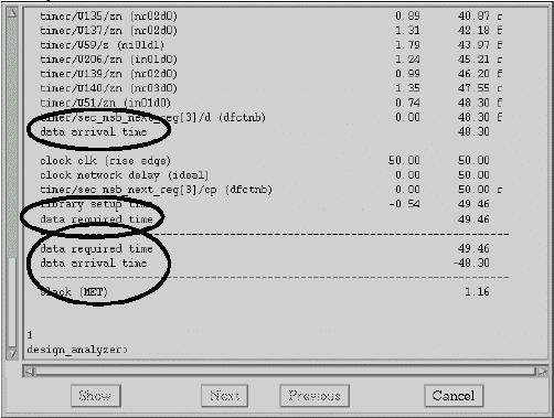
41 Timing Report pp. 41

42 Analyze Circuit with Schematic To determine the time the signal arrived at pin which is selected in the schematic Analysis/Show Timing pp. 42

43 Analyze Circuit with Schematic To determine the net load which selected in the schematic Analysis/Show Net Load pp. 43
44 Save Design Save your design in verilog format, run Verilog gate-level simulation, and we will use Verilog In interface to translate it into OPUS database for place & route If you can t Verilog In, please check assign problem if there is any assignment problem, choose the block & use the dc_shell command as follow to fix it set_fix_multiple_port_nets -all -buffer_constants compile -map_effort medium pp. 44
45 Gate-Level Simulation (Verilog) Write out gate-level netlist File/Save As Verilog (for File format) dc_shell> write -format verilog hierarchy -output chip.vg Get SDF File/Save Info Design timing Select chip.sdf dc_shell> write_sdf version 1.0 -context verilog chip.sdf Modify your testbench file $sdf_annotate ( the_sdf_file_name, top_module_instance_name); Simulation using Verilog-XL >> Verilog chip.vg testbench.v v cell_model.v pp. 45
46 Design Example Ben ACCESS IC LAB
47 Synopsys Design Vision (GUI) / Design Compiler (text mode) Unix% dv dcsh_mode & Unix% dc_shell pp. 47

48 Read Verilog File read -format verilog {"Lab1_alu.v"} pp. 48

49 Schematic view Synopsys Design analyzer will translate verilog code into G-tech model. Double click the icon ALU, and click the right button then choose Schematic view. We can get the G-tech MAP pp. 49

50 Symbol view Or you can create a symbol view by click on the following symbol view button. The symbol view is as the right window pp. 50
 pp.")
51 Attributes - Specify Clock Set Clock (1/2) pp. 51

52 Set Clock (2/2) Specify the clock as period 10ns. (100 MHz). Don t forget to select don t touch network and fix hold create_clock -name "clk" -period 10 -waveform {"0" "5"} {"clk"} set_dont_touch_network find( clock, "clk") set_fix_hold clk pp. 52
53 Operating Condition set_operating_conditions "typical" -library "typical" pp. 53
54 Wireload Model set_wire_load_model -name "ForQA" -library "typical" set_wire_load_mode "segmented" pp. 54

55 Operating Environment Select inputa in the Symbol View and click Attribute - operating environment - input delay. Set 2.5ns input delay. set_input_delay -clock clk 2.5 inputa[*] set_input_delay -clock clk 3.8 inputb[*] set_input_delay -clock clk 4.5 instruction[*] set_input_delay -clock clk 5.2 reset set_output_delay -clock clk 8 alu_out[*] pp. 55

56 Area & Fanout & Transition Click Attribute - optimization Constraints - Design constraints. Set max area is 0. Max fan-out is 8. max transition is 1. set_max_area 0 set_max_fanout 8 find (design, ALU) set_max_transition 1 find (design, ALU) pp. 56

57 Compile Design Click Design - Compile Design. Click OK, start to optimize ALU compile -map_effort medium pp. 57

58 Report report_timing -path full -delay max -max_paths 1 -nworst 1 report_power report_area -nosplit pp. 58
59 Save Files Save gate-level netlist. Select File -> Save As Save your design. Select File - Save Save the timing information. Select File - Save Info - Design Timing, choose sdf format. write -format verilog -hierarchy -output "ALU_s.v" find (design, ALU) write -format db -hierarchy -output "ALU_s.db" find (design, ALU) write_sdf ALU_s.sdf Save script file with the constraints you have made. Use write_script > script_file command or File - Save Info - Design Setup button. Re-run all steps automatically. Use include script_file command or File - Execute Script button. pp. 59
60 gate level simulation Before gate level simulation, $sdf_annotate( top_design.sdf, top_design) must be added after initial in testbench `timescale 1ns/10ps must be added in the 1st line of testbench //RTL simulation Unix% verilog testfixture.v //gate level simulation Unix% verilog testfixture_vg.v v umc18.v pp. 60

61 View wave form Unix% nwave& Open verilog.dump file to see the waveform pp. 61
Graduate Institute of Electronics Engineering, NTU Synopsys Synthesis Overview
 Synopsys Synthesis Overview Lecturer: 沈文中 Date: 2005.05.06 ACCESS IC LAB Introduction Outline Synopsys Graphical Environment Setting Design Environment Setting Design Constraints Design Optimization Finite
Introduction to Design Compiler
 Introduction to Design Compiler Courtesy of Dr. An-Yeu Wu @NTU, CIC/NARL@Taiwan http://csce.uark.edu +1 (479) 575-6043 yrpeng@uark.edu What is Synthesis Synthesis = translation + optimization We will get
Getting a Quick Start 2
 2 Getting a Quick Start 2 This chapter walks you through the basic synthesis design flow (shown in Figure 2-1). You use the same basic flow for both design exploration and design implementation. The following
A. Setting Up the Environment a. ~/ece394 % mkdir synopsys b.
 ECE 394 ASIC & FPGA Design Synopsys Design Compiler and Design Analyzer Tutorial A. Setting Up the Environment a. Create a new folder (i.e. synopsys) under your ece394 directory ~/ece394 % mkdir synopsys
RTL Synthesis using Design Compiler. Dr Basel Halak
 RTL Synthesis using Design Compiler Dr Basel Halak Learning Outcomes: After completing this unit, you should be able to: 1. Set up the DC RTL Synthesis Software and run synthesis tasks 2. Synthesize a
King Fahd University of Petroleum and Minerals. Computer Engineering Department. COE 561 Digital Systems Design and Synthesis (Course Activity)
") King Fahd University of Petroleum and Minerals Computer Engineering Department COE 561 Digital Systems Design and Synthesis (Course Activity) Synthesis using Synopsys Design Compiler Tutorial The Synthesis
King Fahd University of Petroleum and Minerals Computer Engineering Department COE 561 Digital Systems Design and Synthesis (Course Activity) Synthesis using Synopsys Design Compiler Tutorial The Synthesis
Preparing for Optimization 7
 7 Preparing for Optimization 7 This chapter contains the following sections: Defining the Design Environment Selecting a Compile Strategy Setting Design Rule Constraints Setting Optimization Constraints
CS/EE 6710 Digital VLSI Design Tutorial on Cadence to Synopsys Interface (CSI)
") CS/EE 6710 Digital VLSI Design Tutorial on Cadence to Synopsys Interface (CSI) This tutorial walks you through the Cadence to Synopsys Interface (CSI). This interface lets you take a schematic from composer
CS/EE 6710 Digital VLSI Design Tutorial on Cadence to Synopsys Interface (CSI) This tutorial walks you through the Cadence to Synopsys Interface (CSI). This interface lets you take a schematic from composer
Compile RISC_CORE. Learning Objectives. After completing this lab, you should be able to: Perform a top-down compile strategy on the RISC_CORE design
 15 Learning Objectives After completing this lab, you should be able to: Perform a top-down compile strategy on the RISC_CORE design Lab Duration: 75 minutes Lab 15-1 Synopsys 31833-000-S38 Flow Diagram
Logic Synthesis ( Prof. Dejan Marković VLSI Design Flow. Specifications & System Simulation (MATLAB, Simulink, C++)
") Logic Synthesis EEM216A Fall 2012 Prof. Dejan Marković ee216a@gmail.com VLSI Design Flow Specifications & System Simulation (MATLAB, Simulink, C++) RTL Design (Verilog HDL) Logic Synthesis ( DC) Today
Logic Synthesis EEM216A Fall 2012 Prof. Dejan Marković ee216a@gmail.com VLSI Design Flow Specifications & System Simulation (MATLAB, Simulink, C++) RTL Design (Verilog HDL) Logic Synthesis ( DC) Today
Tutorial for Verilog Synthesis Lab (Part 2)
") Tutorial for Verilog Synthesis Lab (Part 2) Before you synthesize your code, you must absolutely make sure that your verilog code is working properly. You will waste your time if you synthesize a wrong
Tutorial for Verilog Synthesis Lab (Part 2) Before you synthesize your code, you must absolutely make sure that your verilog code is working properly. You will waste your time if you synthesize a wrong
Design Rules and Min Timing
 7 Design Rules and Min Timing Learning Objectives After completing this lab, you should be able to: Apply design rules and hold time constraints Fix design rule violations Fix hold time violations Lab
Overview. Design flow. Principles of logic synthesis. Logic Synthesis with the common tools. Conclusions
 Logic Synthesis Overview Design flow Principles of logic synthesis Logic Synthesis with the common tools Conclusions 2 System Design Flow Electronic System Level (ESL) flow System C TLM, Verification,
Laboratory 5. - Using Design Compiler for Synthesis. By Mulong Li, 2013
 CME 342 (VLSI Circuit Design) Laboratory 5 - Using Design Compiler for Synthesis By Mulong Li, 2013 Reference: http://www.tkt.cs.tut.fi/tools/public/tutorials/synopsys/design_compiler/gsdc.html Background
Logic Synthesis. Logic Synthesis. Gate-Level Optimization. Logic Synthesis Flow. Logic Synthesis. = Translation+ Optimization+ Mapping
 Logic Synthesis Logic Synthesis = Translation+ Optimization+ Mapping Logic Synthesis 2 Gate-Level Optimization Logic Synthesis Flow 3 4 Design Compiler Procedure Logic Synthesis Input/Output 5 6 Design
Automated Synthesis from HDL models. Design Compiler (Synopsys) Leonardo (Mentor Graphics)
 Leonardo (Mentor Graphics)") Automated Synthesis from HDL models Design Compiler (Synopsys) Leonardo (Mentor Graphics) Front-End Design & Verification VHDL Verilog SystemC Create Behavioral/RTL HDL Model(s) VHDL-AMS Verilog-A ModelSim
Automated Synthesis from HDL models Design Compiler (Synopsys) Leonardo (Mentor Graphics) Front-End Design & Verification VHDL Verilog SystemC Create Behavioral/RTL HDL Model(s) VHDL-AMS Verilog-A ModelSim
Performing STA. Learning Objectives
 Performing STA Learning Objectives UNIT 45 minutes Unit 8 You are provided with a design netlist that does not meet timing. You are also provided with another set of sub blocks that were improved for timing
DC-Tcl Procedures. Learning Objectives. After completing this lab, you should be able to: Write generic DC-Tcl procedures. Lab Duration: 30 minutes
 w 14 Learning Objectives After completing this lab, you should be able to: Write generic DC-Tcl procedures Lab Duration: 30 minutes Lab 14-1 Synopsys 31833-000-S38 Flow Diagram of Lab Create and test myprocs.tcl
Multiple Clocks and Timing Exceptions
 10 Multiple Clocks and Timing Exceptions Learning Objectives This lab is intended to give you a better understanding of how static timing analysis works and how timing exceptions are properly applied.
EE4415 Integrated Digital Design Project Report. Name: Phang Swee King Matric Number: U066584J
 EE4415 Integrated Digital Design Project Report Name: Phang Swee King Matric Number: U066584J April 10, 2010 Contents 1 Lab Unit 1 2 2 Lab Unit 2 3 3 Lab Unit 3 6 4 Lab Unit 4 8 5 Lab Unit 5 9 6 Lab Unit
Lecture 11 Logic Synthesis, Part 2
 Lecture 11 Logic Synthesis, Part 2 Xuan Silvia Zhang Washington University in St. Louis http://classes.engineering.wustl.edu/ese461/ Write Synthesizable Code Use meaningful names for signals and variables
ECE 551 Design Vision Tutorial
 ECE 551 Design Vision Tutorial ECE 551 Staff Dept of Electrical & Computer Engineering, UW-Madison Lesson 0 Tutorial Setup... 2 Lesson 1 Code Input (Analyze and Elaborate)... 4 Lesson 2 - Simple Synthesis...
Introduction to STA using PT
 Introduction to STA using PT Learning Objectives Given the design, library and script files, your task will be to successfully perform STA using the PrimeTime GUI and generate reports. After completing
Specifying Timing Exceptions
 Specifying Timing Exceptions Learning Objectives This lab is intended to give you a better understanding of how static timing analysis works and how timing exceptions are applied properly. After completing
Partitioning for Better Synthesis Results
 3 Partitioning for Better Synthesis Results Learning Objectives After completing this lab, you should be able to: Use the group and ungroup commands to repartition a design within Design Analyzer Analyze
Setup file.synopsys_dc.setup
 Setup file.synopsys_dc.setup The.synopsys_dc.setup file is the setup file for Synopsys' Design Compiler. Setup file is used for initializing design parameters and variables, declare design libraries, and
HOW TO SYNTHESIZE VERILOG CODE USING RTL COMPILER
 HOW TO SYNTHESIZE VERILOG CODE USING RTL COMPILER This tutorial explains how to synthesize a verilog code using RTL Compiler. In order to do so, let s consider the verilog codes below. CNT_16 Module: 16
SmartTime for Libero SoC v11.5
 SmartTime for Libero SoC v11.5 User s Guide NOTE: PDF files are intended to be viewed on the printed page; links and cross-references in this PDF file may point to external files and generate an error
PrimeTime: Introduction to Static Timing Analysis Workshop
 i-1 PrimeTime: Introduction to Static Timing Analysis Workshop Synopsys Customer Education Services 2002 Synopsys, Inc. All Rights Reserved PrimeTime: Introduction to Static 34000-000-S16 Timing Analysis
Push-button Synthesis or, Using dc_perl to do_the_right_thing
 Push-button Synthesis or, Using dc_perl to do_the_right_thing Kurt Baty WSFDB Consulting 26 Hill Street Medway MA 02053 Phone: +1.508.429.4198 Email: kurt@wsfdb.com Steve Golson Trilobyte Systems 33 Sunset
Agenda: Day Two. Unit 6: Specifying Timing Exceptions DAY 2. I/O Paths and Exceptions. Constraining I/O Interface Paths
 Agenda: Day Two 6-1 DAY 2 Unit I/O Paths and Exceptions Lab 5 Constraining I/O Interface Paths 6 7 Introduction to Timing Models (QTM) 8 Performing STA 9 Summary 10 Customer Support 6-1 Unit 6: Unit Objectives
Hardware Verification Group. Department of Electrical and Computer Engineering, Concordia University, Montreal, Canada. CAD Tool Tutorial.
 Digital Logic Synthesis and Equivalence Checking Tools Hardware Verification Group Department of Electrical and Computer Engineering, Concordia University, Montreal, Canada CAD Tool Tutorial May, 2010
Pipelined MIPS CPU Synthesis and On-Die Representation ECE472 Joseph Crop Stewart Myers
 Pipelined MIPS CPU Synthesis and On-Die Representation ECE472 Joseph Crop Stewart Myers 2008 Table of Contents Introduction... 3 Steps Taken and Simulation... 3 Pitfalls... 8 Simulated Delay... 9 APPENDIX
Part B. Dengxue Yan Washington University in St. Louis
 Tools Tutorials Part B Dengxue Yan Washington University in St. Louis Tools mainly used in this class Synopsys VCS Simulation Synopsys Design Compiler Generate gate-level netlist Cadence Encounter placing
ECE 4514 Digital Design II. Spring Lecture 20: Timing Analysis and Timed Simulation
 ECE 4514 Digital Design II Lecture 20: Timing Analysis and Timed Simulation A Tools/Methods Lecture Topics Static and Dynamic Timing Analysis Static Timing Analysis Delay Model Path Delay False Paths Timing
Virtex 2.1i tutorial: Verilog using FPGA Compiler and VerilogXL
 Virtex 2.1i tutorial: Verilog using FPGA Compiler and VerilogXL This tutorial describes the Virtex design flow with Synopsys FPGA Compiler, and simulation flow with VerilogXL simulator. It includes the
Introduction to Design With Verilog. Synopsys University Courseware 2008 Synopsys, Inc. Lecture - 3 Developed By: Paul D. Franzon
 Introduction to Design With Verilog Course Mantras One clock, one edge, Flip-flops only Design BEFORE coding Behavior implies function Clearly separate control and datapath Purpose of HDLs Purpose of Hardware
Cell-Based Design Flow. TA : 吳廸優
 Cell-Based Design Flow TA : 吳廸優 dywu@viplab.cs.nctu.edu.tw 1 Outline Overview Design Flow Stage 1 RTL Development Synthesis Gate Level Simulation Design Flow Stage 2 Placement and Routing Post Layout Simulation
Behavioral Modeling and Timing Constraints
 Introduction Behavioral modeling was introduced in Lab 1 as one of three widely used modeling styles. Additional capabilities with respect to testbenches were further introduced in Lab 4. However, there
A Comparison of Hierarchical Compile Strategies
 A Comparison of Hierarchical Compile Strategies Steve Golson Trilobyte Systems 33 Sunset Road Carlisle MA 01741 Phone: +1.978.369.9669 Fax: +1.978.371.9964 Email: sgolson@trilobyte.com http://www.trilobyte.com
EE183 LAB TUTORIAL. Introduction. Projects. Design Entry
 EE183 LAB TUTORIAL Introduction You will be using several CAD tools to implement your designs in EE183. The purpose of this lab tutorial is to introduce you to the tools that you will be using, Xilinx
EE 5327 VLSI Design Laboratory Lab 8 (1 week) Formal Verification
 Formal Verification") EE 5327 VLSI Design Laboratory Lab 8 (1 week) Formal Verification PURPOSE: To use Formality and its formal techniques to prove or disprove the functional equivalence of two designs. Formality can be used
EE 5327 VLSI Design Laboratory Lab 8 (1 week) Formal Verification PURPOSE: To use Formality and its formal techniques to prove or disprove the functional equivalence of two designs. Formality can be used
Verilog for High Performance
 Verilog for High Performance Course Description This course provides all necessary theoretical and practical know-how to write synthesizable HDL code through Verilog standard language. The course goes
LECTURE 5: VHDL SYNTHESIS with SYNOPSYS dc_shell
 EECS 317 CAD Computer Design LECTURE 5: VHDL SYNTHESIS with SYNOPSYS dc_shell Instructor: Francis G. Wolff wolff@eecs.cwru.edu Case Western Reserve University This presentation uses powerpoint animation:
EECS 151/251A ASIC Lab 6: Power and Timing Verification
 EECS 151/251A ASIC Lab 6: Power and Timing Verification Written by Nathan Narevsky (2014,2017) and Brian Zimmer (2014) Modified by John Wright (2015,2016), Ali Moin (2017) and Taehwan Kim (2018) Overview
1 Design Process HOME CONTENTS INDEX. For further assistance, or call your local support center
 1 Design Process VHDL Compiler, a member of the Synopsys HDL Compiler family, translates and optimizes a VHDL description to an internal gate-level equivalent. This representation is then compiled with
FishTail: The Formal Generation, Verification and Management of Golden Timing Constraints
 FishTail: The Formal Generation, Verification and Management of Golden Timing Constraints Chip design is not getting any easier. With increased gate counts, higher clock speeds, smaller chip sizes and
CPE/EE 427, CPE 527, VLSI Design I: Tutorial #4, Standard cell design flow (from verilog to layout, 8-bit accumulator)
") CPE/EE 427, CPE 527, VLSI Design I: Tutorial #4, Standard cell design flow (from verilog to layout, 8-bit accumulator) Joel Wilder, Aleksandar Milenkovic, ECE Dept., The University of Alabama in Huntsville
CPE/EE 427, CPE 527, VLSI Design I: Tutorial #4, Standard cell design flow (from verilog to layout, 8-bit accumulator) Joel Wilder, Aleksandar Milenkovic, ECE Dept., The University of Alabama in Huntsville
Hardware Verification Group
 Digital Logic Synthesis and Equivalence Checking Tools Tutorial Hardware Verification Group Department of Electrical and Computer Engineering, Concordia University, Montreal, Canada {n ab, h aridh}@encs.concordia.ca
Cell-Based Design Flow. 林丞蔚
 Cell-Based Design Flow 林丞蔚 cultom@viplab.cs.nctu.edu.tw 1 Outline Overview Design Flow 1 RTL Development Synthesis Gate Level Simulation Design Flow 2 Placement and Routing Example Design IC Contest 2006
Altera/Synopsys User Guide
 Altera/Synopsys User Guide About this User Guide July 1995 This user guide provides design guidelines, sample VHDL designs, Altera-specific design methods, and optimal synthesis options to assist designers
Post-Synthesis Simulation. VITAL Models, SDF Files, Timing Simulation
 Post-Synthesis Simulation VITAL Models, SDF Files, Timing Simulation Post-synthesis simulation Purpose: Verify correctness of synthesized circuit Verify synthesis tool delay/timing estimates Synthesis
EECS 151/251A ASIC Lab 3: Logic Synthesis
 EECS 151/251A ASIC Lab 3: Logic Synthesis Written by Nathan Narevsky (2014, 2017) and Brian Zimmer (2014) Modified by John Wright (2015,2016) and Taehwan Kim (2018) Overview For this lab, you will learn
Altera Quartus II Synopsys Design Vision Tutorial
 Altera Quartus II Synopsys Design Vision Tutorial Part III ECE 465 (Digital Systems Design) ECE Department, UIC Instructor: Prof. Shantanu Dutt Prepared by: Xiuyan Zhang, Ouwen Shi In tutorial part II,
Logic Verification 13-1
 Logic Verification 13-1 Verification The goal of verification To ensure 100% correct in functionality and timing Spend 50 ~ 70% of time to verify a design Functional verification Simulation Formal proof
UNIVERSITY OF CALIFORNIA, DAVIS Department of Electrical and Computer Engineering. EEC180A DIGITAL SYSTEMS I Winter 2015
 UNIVERSITY OF CALIFORNIA, DAVIS Department of Electrical and Computer Engineering EEC180A DIGITAL SYSTEMS I Winter 2015 LAB 1: Introduction to Quartus II Schematic Capture and ModelSim Simulation This
Synthesis and APR Tools Tutorial
 Synthesis and APR Tools Tutorial (Last updated: Oct. 26, 2008) Introduction This tutorial will get you familiarized with the design flow of synthesizing and place and routing a Verilog module. All the
Timing Analyzer Quick-Start Tutorial
 Timing Analyzer Quick-Start Tutorial Intel Quartus Prime Pro Edition Updated for Intel Quartus Prime Design Suite: 17.1 Subscribe Send Feedback Latest document on the web: PDF HTML Contents Contents Timing
TRILOBYTE SYSTEMS. Consistent Timing Constraints with PrimeTime. Steve Golson Trilobyte Systems.
 TRILOBYTE SYSTEMS Consistent Timing Constraints with PrimeTime Steve Golson Trilobyte Systems http://www.trilobyte.com 2 Physical implementation Rule #1 Do not change the functionality Rule #2 Meet the
Timing Constraints Editor User Guide
 Libero SoC v11.8 SP1 and SP2 NOTE: PDF files are intended to be viewed on the printed page; links and cross-references in this PDF file may point to external files and generate an error when clicked. View
Writing Circuit Descriptions 8
 8 Writing Circuit Descriptions 8 You can write many logically equivalent descriptions in Verilog to describe a circuit design. However, some descriptions are more efficient than others in terms of the
A GENERATION AHEAD SEMINAR SERIES
 A GENERATION AHEAD SEMINAR SERIES Constraints &Tcl Scripting Design Methodology Guidelines for Faster Timing Convergence Agenda Vivado Tcl Overview XDC Management Design Methodology for Faster Timing Closure
VHDL for Synthesis. Course Description. Course Duration. Goals
 VHDL for Synthesis Course Description This course provides all necessary theoretical and practical know how to write an efficient synthesizable HDL code through VHDL standard language. The course goes
An overview of standard cell based digital VLSI design
 An overview of standard cell based digital VLSI design Implementation of the first generation AsAP processor Zhiyi Yu and Tinoosh Mohsenin VCL Laboratory UC Davis Outline Overview of standard cellbased
Tutorial 2.(b) : Synthesizing your design using the Synopsys Design Compiler ( For DFT Flow)
 : Synthesizing your design using the Synopsys Design Compiler ( For DFT Flow)") Tutorial 2.(b) : Synthesizing your design using the Synopsys Design Compiler ( For DFT Flow) Objectives: In this tutorial you will learrn to use Synopsys Design Compiler (DC) to perform hardware synthesis
Tutorial 2.(b) : Synthesizing your design using the Synopsys Design Compiler ( For DFT Flow) Objectives: In this tutorial you will learrn to use Synopsys Design Compiler (DC) to perform hardware synthesis
Actel Libero TM Integrated Design Environment v2.3 Structural Schematic Flow Design Tutorial
 Actel Libero TM Integrated Design Environment v2.3 Structural Schematic Flow Design Tutorial 1 Table of Contents Design Flow in Libero TM IDE v2.3 Step 1 - Design Creation 3 Step 2 - Design Verification
Timing Analysis in Xilinx ISE
 Timing Analysis in Xilinx ISE For each design which is to be implemented, constraints should be defined to get predictable results. The first important class of constraints was already introduced in the
101-1 Under-Graduate Project Digital IC Design Flow
 101-1 Under-Graduate Project Digital IC Design Flow Speaker: Ming-Chun Hsiao Adviser: Prof. An-Yeu Wu Date: 2012/9/25 ACCESS IC LAB Outline Introduction to Integrated Circuit IC Design Flow Verilog HDL
EKT 422/4 COMPUTER ARCHITECTURE. MINI PROJECT : Design of an Arithmetic Logic Unit
 EKT 422/4 COMPUTER ARCHITECTURE MINI PROJECT : Design of an Arithmetic Logic Unit Objective Students will design and build a customized Arithmetic Logic Unit (ALU). It will perform 16 different operations
The Boa Methodology. Abstract. What is Boa? by Wilson Snyder, Digital Semiconductor, January 17, 1997
 The Boa Methodology 1 of 15 The Boa Methodology by Wilson Snyder, Digital Semiconductor, January 17, 1997 Abstract The Synopsys methodology devised by Digital Semiconductor called the "Boa Methodology"
ENGN 1630: CPLD Simulation Fall ENGN 1630 Fall Simulating XC9572XLs on the ENGN1630 CPLD-II Board Using Xilinx ISim
 ENGN 1630 Fall 2018 Simulating XC9572XLs on the ENGN1630 CPLD-II Board Using Xilinx ISim You will use the Xilinx ISim simulation software for the required timing simulation of the XC9572XL CPLD programmable
E85: Digital Design and Computer Engineering Lab 2: FPGA Tools and Combinatorial Logic Design
 E85: Digital Design and Computer Engineering Lab 2: FPGA Tools and Combinatorial Logic Design Objective The purpose of this lab is to learn to use Field Programmable Gate Array (FPGA) tools to simulate
Cadence Tutorial 6. Verilog-XL Simulation for Dynamic Logic. EE577b Fall 98
 Cadence Tutorial 6 Verilog-XL Simulation for Dynamic Logic EE577b Fall 98 In this tutorial, I am going to demonstrate how to design and simulate the domino style dynamic logic. 1. Tutorial Setup No previous
Synthesis. Other key files. Standard cell (NAND, NOR, Flip-Flop, etc.) FPGA CLB
 FPGA CLB") SYNTHESIS Synthesis Involves synthesizing a gate netlist from verilog source code We use Design Compiler (DC) by Synopsys which is the most popular synthesis tool used in industry Target library examples:
SYNTHESIS Synthesis Involves synthesizing a gate netlist from verilog source code We use Design Compiler (DC) by Synopsys which is the most popular synthesis tool used in industry Target library examples:
EE 361L Digital Systems and Computer Design Laboratory
 University of Hawaii Department of Electrical Engineering EE 361L Digital Systems and Computer Design Laboratory Timing Simulation Version 1.0 10/10/2003 This document is a quick tutorial on performing
Laboratory Exercise 3
 Laboratory Exercise 3 Latches, Flip-flops, and egisters The purpose of this exercise is to investigate latches, flip-flops, and registers. Part I Altera FPGAs include flip-flops that are available for
CMOS VLSI Design Lab 3: Controller Design and Verification
 CMOS VLSI Design Lab 3: Controller Design and Verification The controller for your MIPS processor is responsible for generating the signals to the datapath to fetch and execute each instruction. It lacks
Top-down digital design flow
 6 Dec 2005 Top-down digital design flow EDA tools: Modelsim, Synopsys Design Compiler, Cadence Encounter Alain Vachoux Microelectronic Systems Lab STI-IMM-LSM alain.vachoux@epfl.ch version 3.0.2 / 6 Dec
TOPIC : Verilog Synthesis examples. Module 4.3 : Verilog synthesis
 TOPIC : Verilog Synthesis examples Module 4.3 : Verilog synthesis Example : 4-bit magnitude comptarator Discuss synthesis of a 4-bit magnitude comparator to understand each step in the synthesis flow.
DE2 Board & Quartus II Software
 January 23, 2015 Contact and Office Hours Teaching Assistant (TA) Sergio Contreras Office Office Hours Email SEB 3259 Tuesday & Thursday 12:30-2:00 PM Wednesday 1:30-3:30 PM contre47@nevada.unlv.edu Syllabus
Constraint Verification
 Constraint Verification Constraint verification refers to the verification of the contents of an SDC file to flag situations where the specified constraints are either incorrect, or incomplete, both of
ESE 570 Cadence Lab Assignment 2: Introduction to Spectre, Manual Layout Drawing and Post Layout Simulation (PLS)
") ESE 570 Cadence Lab Assignment 2: Introduction to Spectre, Manual Layout Drawing and Post Layout Simulation (PLS) Objective Part A: To become acquainted with Spectre (or HSpice) by simulating an inverter,
ESE 570 Cadence Lab Assignment 2: Introduction to Spectre, Manual Layout Drawing and Post Layout Simulation (PLS) Objective Part A: To become acquainted with Spectre (or HSpice) by simulating an inverter,
Advanced FPGA Design. Jan Pospíšil, CERN BE-BI-BP ISOTDAQ 2018, Vienna
 Advanced FPGA Design Jan Pospíšil, CERN BE-BI-BP j.pospisil@cern.ch ISOTDAQ 2018, Vienna Acknowledgement Manoel Barros Marin (CERN) lecturer of ISOTDAQ-17 Markus Joos (CERN) & other organisers of ISOTDAQ-18
Intel Quartus Prime Standard Edition User Guide
 Intel Quartus Prime Standard Edition User Guide Timing Analyzer Updated for Intel Quartus Prime Design Suite: 18.1 Subscribe Latest document on the web: PDF HTML Contents Contents 1. Timing Analysis Introduction...
EE 466/586 VLSI Design. Partha Pande School of EECS Washington State University
 EE 466/586 VLSI Design Partha Pande School of EECS Washington State University pande@eecs.wsu.edu Lecture 18 Implementation Methods The Design Productivity Challenge Logic Transistors per Chip (K) 10,000,000.10m
Standard Cell Based Design Flow Using Modelsim, Buildgates, and Silicon Ensemble
 Arifur Rahman, Spring 2004, Polytechnic University, NY Standard Cell Based Design Flow Using Modelsim, Buildgates, and Silicon Ensemble Mapped Netlist Back Annotation using SDF File and mapped netlist
EE 330 Spring Laboratory 2: Basic Boolean Circuits
 EE 330 Spring 2013 Laboratory 2: Basic Boolean Circuits Objective: The objective of this experiment is to investigate methods for evaluating the performance of Boolean circuits. Emphasis will be placed
LSN 1 Digital Design Flow for PLDs
 LSN 1 Digital Design Flow for PLDs ECT357 Microprocessors I Department of Engineering Technology LSN 1 Programmable Logic Devices Functionless devices in base form Require programming to operate The logic
Engineering 1630 Fall Simulating XC9572XL s on the ENGN1630 CPLD-II Board
 Engineering 1630 Fall 2016 Simulating XC9572XL s on the ENGN1630 CPLD-II Board You will use the Aldec Active-HDL software for the required timing simulation of the XC9572XL CPLD programmable logic chips
Applications Note. HDL Simulation FPGA Design Methodology. October 15, Revision 1.0
 Applications Note HDL Simulation FPGA Design Methodology October 15, 1998 Revision 1.0 OVERVIEW... 3 MODEL TECHNOLOGY, EXEMPLAR & XILINX TOOLFLOW OVERVIEW... 3 SYNTHESIS PROCESS DESIGN FLOW... 4 EXAMPLE
Don t expect to be able to write and debug your code during the lab session.
 EECS150 Spring 2002 Lab 4 Verilog Simulation Mapping UNIVERSITY OF CALIFORNIA AT BERKELEY COLLEGE OF ENGINEERING DEPARTMENT OF ELECTRICAL ENGINEERING AND COMPUTER SCIENCE Lab 4 Verilog Simulation Mapping
Logic Circuits II ECE 2411 Thursday 4:45pm-7:20pm. Lecture 3
 Logic Circuits II ECE 2411 Thursday 4:45pm-7:20pm Lecture 3 Lecture 3 Topics Covered: Chapter 4 Discuss Sequential logic Verilog Coding Introduce Sequential coding Further review of Combinational Verilog
Vivado Design Suite User Guide
 Vivado Design Suite User Guide Synthesis Revision History The following table shows the revision history for this document: Date Version Revision 06/24/2015 2015.2 Changes are: Added Important note on
AccuCore SPICE Accurate Core Characterization with STA. Silvaco Japan Technology Seminar Spring 2007
 AccuCore SPICE Accurate Core Characterization with STA Silvaco Japan Technology Seminar Spring 2007 What is AccuCore? Why would I use it? AccuCore performs automatic block SPICE characterization and Static
AccuCore. Product Overview of Block Characterization, Modeling and STA
 AccuCore Product Overview of Block Characterization, Modeling and STA What is AccuCore? AccuCore performs timing characterization of multi-million device circuits with SmartSpice accuracy and performs
Experiment VERI: FPGA Design with Verilog (Part 2) (webpage: /)
 (webpage: /)") Department of Electrical & Electronic Engineering 2 nd Year Laboratory Experiment VERI: FPGA Design with Verilog (Part 2) (webpage: www.ee.ic.ac.uk/pcheung/teaching/e2_experiment /) 1.0 Learning Outcomes
Department of Electrical & Electronic Engineering 2 nd Year Laboratory Experiment VERI: FPGA Design with Verilog (Part 2) (webpage: www.ee.ic.ac.uk/pcheung/teaching/e2_experiment /) 1.0 Learning Outcomes
HDL Compiler Directives 7
 7 HDL Compiler Directives 7 Directives are a special case of regular comments and are ignored by the Verilog HDL simulator HDL Compiler directives begin, like all other Verilog comments, with the characters
ESE 570 Cadence Lab Assignment 1: Logic Simulation in Verilog-XL
 ESE 570 Cadence Lab Assignment 1: Logic Simulation in Verilog-XL Exercises Part A i. CMOS inverter Schematic Description Yang Lu, Department of Material Science and Engineering Symbol Description Functional
An easy to read reference is:
 1. Synopsis: Timing Analysis and Timing Constraints The objective of this lab is to make you familiar with two critical reports produced by the Xilinx ISE during your design synthesis and implementation.
Two HDLs used today VHDL. Why VHDL? Introduction to Structured VLSI Design
 Two HDLs used today Introduction to Structured VLSI Design VHDL I VHDL and Verilog Syntax and ``appearance'' of the two languages are very different Capabilities and scopes are quite similar Both are industrial