Prototype of SRAM by Sergey Kononov, et al.
|
|
|
- Maurice Augustine Eaton
- 5 years ago
- Views:
Transcription
1 Prototype of SRAM by Sergey Kononov, et al.
2 1. Project Overview The goal of the project is to create a SRAM memory layout that provides maximum utilization of the space on the 1.5 by 1.5 mm chip. Significant portion of that space is dedicated to the I/O Pads, living approximately 1 mm^2 for the memory array and the control circuitry. The size of the basic memory cell is, for the most part, dictated by the type of the technology used to produce the chip. The calculation provided in the memory array block description have shown that in the most optimal case up to 4 Kbits of the 6-transistor CMOS memory cells can be fitted on the space provided, living very limited amount of space for the rest of the logic gates that need to be placed on the chip. The Figure 1.1 shows the locations of each of the blocks on the chip. Figure1.1 Block Locations The chip features 4 kilobytes of the SRAM CMOS memory. The logical representation of the memory array has 32 rows and 128 columns. In order to fit all of the memory cells on the chip 32 of these columns have been placed on the chip as a separate block. Besides memory storage the chip contains several other blocks that provide functionality necessary to access and maintain the data stored in the array. The memory read operation is self-timed. This is accomplished through the use of the timing pulse that is generated every time the new address is put on the data lines. It is used by the precharging block as well as the control blocks to determined when it is time to initialize the necessary transactions. The precharging block is responsible for the equalizing and the precharging of the bit lines of the chosen column to 5V. Once the column is pre-charged the proper row is selected and the data becomes available to the associated sense amplifiers. At every transaction 8 bits of the memory are accessed and fed into the 8 sense amplifiers, which allow to read the data as soon as the voltage difference on the lines becomes appropriate. This voltage difference is significantly smaller then would be required if
3 the data was accessed without the use of the sense amplifiers. This acquired speed-up is the primarily reason for the use of the sense amplifiers on the chip. The access of the columns and rows is done using row and column decoders. In order to minimize the required space, the corresponding decoders are implemented 2 and 3-bit predecoders, the outputs of which are fed into 2-bit AND gates located at the foundation of the memory array. 2. Block description Memory Cell The memory cell layout and schematic are provided in the figures 2.1 and 2.2 accordingly. Figure 2.1 Memory Cell Layout There are two main concerns when designing the memory cell. One is to guarantee that once the precharging is done and the pass transistors of the cells are enabled that initial voltage spike on the negative bit line does not cause the transition of the cell into the opposite state. Such situation is prevented through the sizing of the n-transistors and pass-transistors of the memory cells in a way that guarantees that the voltage across the pmos transistors never drops below threshold value. To achieve this, their width-to-length(w/l) sizes has to satisfy the values calculated using the formulas below. These formulas are the result of the equating of the currents of the involved transistors at the critical stages. Once the required ratio for the nmos to pass transistor sizing is established it becomes impossible to write to the cell by puling the zero bit line up, which means that the writing to the cell is done by pulling the positive bit line down. In order for this to happen the proper ratio has to exist between the W/L sizes of the pass and pmos transistors of the cell. The second set of
_pass/(WL)_nmos < (2(V_DDV_TN)-3V_TN^2)/(V_DD-2V_TN)^2=0.")
4 calculation establishes the required ratio. The results below were calculated using following values: V_DD=5V; V_TN=0.66; V_TP=-0.915; k_n/k_p=2 The ratio of the W/L values of the pass transistors to nmos transistors of the memory cell has to be: (W/L)_pass/(WL)_nmos < (2(V_DDV_TN)-3V_TN^2)/(V_DD-2V_TN)^2=0.39 The ratio of the W/L values of the pmos transistor to the pass transistors has to be: (W/L)_pmos/(WL)_pass < k_n'/k_p' *(2(V_DDV_TN)- 3V_TN^2)/(V_DD+V_TP)^2=0.63 As a result the W/L ratio PMOS transistors has to be approximately ¼ of the NMOS transistors: P_MOS=0.63*0.39=1/4NMOS The values picked in order to achieve required ratios were: NMOS PMOS PASS 1800/ / /750 Figure 2.2 Memory Cell Schematic Due to the crucial role of the proper sizing of all involved transistors in the whole datapath, the testing of the memory cells and associated peripheral cells was done in a form of a single test. The description of this test and the associated waveform is provided in the document after the description of all of the cells used in the test. Precharger.

5 The significant portion of the read and write cycles is dedicated to the decoding of the address. Once the address of the cell is decoded the reading and writing process starts. Without sense amplifiers in order to guarantee that the proper values were read, the end of these cycles would have to be delayed to guarantee that the bit lines reach the rail voltages. The sense amplifiers allow to avoid such delays through amplification of the difference between the bit lines. In order to do this reliably and fast, they require the input voltages to be equalized to some predetermined value. This functionality in the circuitry is provided by the precharger cells. The schematic and the layout of that cells are presented in the Figures 2.3 and 2.4 accordingly. Figure 2.3
, so that once the minimum required voltage difference is reached the evaluations goes into the second stage, during which this difference is amplified and")
6 Figure 2.4 Sense amplifier. This block provides 2 stage amplification. During first stage the input voltages are first equalized and shifted to the 2.5 voltage value. The circuit is timed(using global pulse), so that once the minimum required voltage difference is reached the evaluations goes into the second stage, during which this difference is amplified and outputted to the tristate buffer. The schematics of the both stages and the corresponding layout is presented in the figures 2.5 and 2.6.


7 Figure 2.5 Figure 2.6 Test of the memory cells. The testing of the circuitry has been done using single

8 memory, sense amplifier, pass transistor and the precharger cells. In order to do the proper simulation the capacitance is attached to the bit line inputs. The capacitance is placed to account for the parasitic capacitance resulting from the connection of the bit line to 32 cells that each memory column is made of. The testing is done in two stages: during first stage the ability of the set-up to change the value in the circuit by pulling the positive line down is tested. Then the ability to output proper(inverted) values is tested. The resulting waveform is presented in Figure Figures show the schematic, layout and test bench circuits used for simulation. Due to the fact that the result of the schematic is dependent upon the sizing of the transistors and the fact that the minimum size that could be set up on the schematic is greater then actual values used in the circuit, only the simulation of the extracted layout was done. Figure 2.7 Schematic of the circuit for the test of memory cell.


9 Figure 2.8. Layout of the test circuit for the memory cell Figure 2.9 Test bench for the memory cell

10 Figure 2.10 Timing of the memory cell On the timing diagram the following waveforms are shown: Pulse is the signal that is used to control the precharging and equalizing stage of the reading cycle. When the pulse cycle is high the precharging and equalizing of the bit lines is done. In order to ensure the proper reading of the data stored in the memory cell, this pulse has to be wide enough to guarantee that both of the bit lines(bl and Bln) are equal to 5V. The time it takes to precharge bit line from zero to 5 V establishes the minimum width of the pulse. Delayed pulse is the signal that is used to control each of the sense amplification cells. It is created inside each of the sense amplification cells. It provides the same functionality for the sense amplification cells as the pulse signal for the precharging cell. It provides a
11 way to slightly delay the sense reading of the values on the bit lines. The stored and stored_b signals are the actual voltages inside the memory cell. The Bl and Bln are the signals that correspond to the bit lines. These lines are connected to the memory cell through the pass transistors that are controlled by the word line. They are also connected to the i/o lines through the column pass transistor. I/O signals are the signals that are produced on the lines connecting memory cell with the sense amplifier and the write circuitry. The writing is done by pulling one of this lines down and the other line up and enabling the column pass transistors. In the test the column pass transistors are always enabled. The output signal it the value that is used to drive the tristate output buffer. During the high stage of the delayed pulse the output is at high Z value. When the sensing occurs it is established to the inverse of the stored value. The output_b signal is the actual signal generated inside the sense amplifier. It drives the output signal described above. As can be seen from the waveform during the precharge stage it is shifted to the 2.5V volts. Once the pulse goes low the sense amplifier drives it to the inverse of the voltage stored in the memory cell. At this point it is connected to the output circuitry. The 5-bit line and 4-bit column decoders are both implemented using 2 stages: the stage of predecoders and the stage 2-bit AND gates. The column decoder uses 2 2-bit predecoders, and the line decoder uses one 2-bit and one 3-bit predecoder. In the case of the line decoder the outputs from the predecoder cells are used to drive the associated word lines of the memory array, while the column decoders are activated in groups of eight and are used to drive the pass cells located in the pass block that control access between the bit lines of the columns of the memory array and the i/o lines.the following pictures contain the layouts and schematics of the decoder circuitry cells


12 Figure 2.11 Pass gate Figure 2.12 Pass gate

13 Figure bit predecoders Figure bit predecoders

14 Figure 2.15 One 3-bit predecoder
15 Figure 2.16 One 3-bit predecoder Pulse generator One of the main components of the control circuitry is the pulse generator. It is implemented using 8 xor gates that are connected to two inputs:the address lines and their delayed equivalent. Once the signal on any of the address lines changes the output of the xor gates goes high due to the fact that it takes time for the delayed signal to catch up with the primary value. The circuitry is presented in the Figure 2.17.

16 Figure 2.17 Pulse generator In order to prevent the unnecessary switching when the chip is not selected the input from the input address buffer into the pulse generator is maintained at the same value through the use of the intermediate latch, controlled by the chip enable signal. This way as soon as the chip is enabled the pulse will be generated if the address is different from previous cycle when the chip was enabled. Otherwise the valid values are already stored in the output buffer and no additional action is required except for enabling the output buffer.

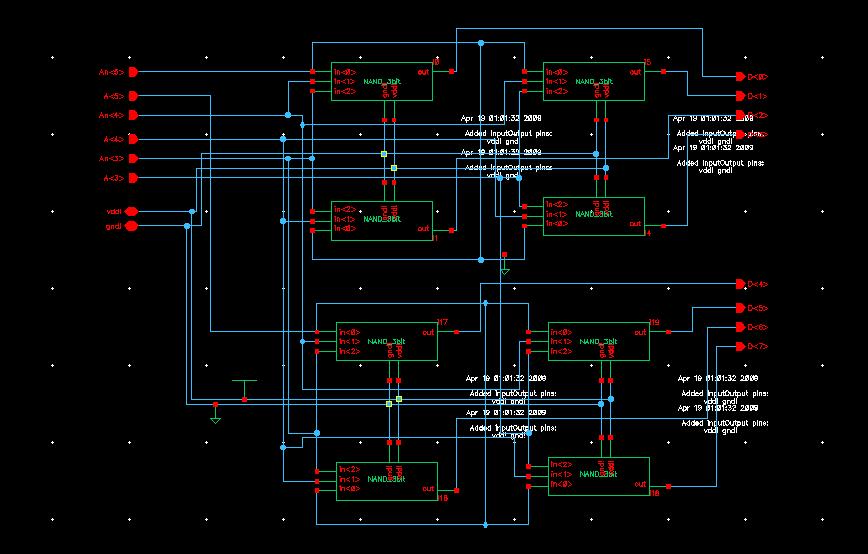
17 3. Dual Port SRAM SRAM cell redesigned for dual port operation. The dual port consists of two read ports and one write port. The six transistor SRAM cell is replaced by a positive edge triggered D-flip flop with two tri-state inverting buffers. Overall memory consists of 32X32 array, accessible in 8bit data width (total 128 bytes). Figure 2.18 Rev 1 SRAM cell consisting of a positive edge triggered D-flip flop with two tri-state inverting buffers.

18 Figure 2.19 Rev 2 SRAM cell consisting of a positive edge triggered D-flip flop with two tri-state inverting buffers.

19 Figure 2.20 Rev 3 SRAM cell consisting of a positive edge triggered D-flip flop with two tri-state inverting buffers.

20 Figure 2.21 Rev 3 SRAM cell data switching simulation.

21 Figure 2.22 Complete 32X32 dual port SRAM block.
Integrated Circuits & Systems
 Federal University of Santa Catarina Center for Technology Computer Science & Electronics Engineering Integrated Circuits & Systems INE 5442 Lecture 23-1 guntzel@inf.ufsc.br Semiconductor Memory Classification
Semiconductor Memory Classification
 ESE37: Circuit-Level Modeling, Design, and Optimization for Digital Systems Lec 6: November, 7 Memory Overview Today! Memory " Classification " Architecture " Memory core " Periphery (time permitting)!
ESE370: Circuit-Level Modeling, Design, and Optimization for Digital Systems
 ESE370: Circuit-Level Modeling, Design, and Optimization for Digital Systems Lec 26: November 9, 2018 Memory Overview Dynamic OR4! Precharge time?! Driving input " With R 0 /2 inverter! Driving inverter
MEMORIES. Memories. EEC 116, B. Baas 3
 MEMORIES Memories VLSI memories can be classified as belonging to one of two major categories: Individual registers, single bit, or foreground memories Clocked: Transparent latches and Flip-flops Unclocked:
Column decoder using PTL for memory
 IOSR Journal of Electronics and Communication Engineering (IOSR-JECE) e-issn: 2278-2834,p- ISSN: 2278-8735. Volume 5, Issue 4 (Mar. - Apr. 2013), PP 07-14 Column decoder using PTL for memory M.Manimaraboopathy
! Memory. " RAM Memory. " Serial Access Memories. ! Cell size accounts for most of memory array size. ! 6T SRAM Cell. " Used in most commercial chips
 ESE 57: Digital Integrated Circuits and VLSI Fundamentals Lec : April 5, 8 Memory: Periphery circuits Today! Memory " RAM Memory " Architecture " Memory core " SRAM " DRAM " Periphery " Serial Access Memories
STUDY OF SRAM AND ITS LOW POWER TECHNIQUES
 INTERNATIONAL JOURNAL OF ELECTRONICS AND COMMUNICATION ENGINEERING & TECHNOLOGY (IJECET) International Journal of Electronics and Communication Engineering & Technology (IJECET), ISSN ISSN 0976 6464(Print)
Introduction to Semiconductor Memory Dr. Lynn Fuller Webpage:
 ROCHESTER INSTITUTE OF TECHNOLOGY MICROELECTRONIC ENGINEERING Introduction to Semiconductor Memory Webpage: http://people.rit.edu/lffeee 82 Lomb Memorial Drive Rochester, NY 14623-5604 Tel (585) 475-2035
Dynamic CMOS Logic Gate
 Dynamic CMOS Logic Gate In dynamic CMOS logic a single clock can be used to accomplish both the precharge and evaluation operations When is low, PMOS pre-charge transistor Mp charges Vout to Vdd, since
Semiconductor Memory Classification. Today. ESE 570: Digital Integrated Circuits and VLSI Fundamentals. CPU Memory Hierarchy.
 ESE 57: Digital Integrated Circuits and VLSI Fundamentals Lec : April 4, 7 Memory Overview, Memory Core Cells Today! Memory " Classification " ROM Memories " RAM Memory " Architecture " Memory core " SRAM
CENG 4480 L09 Memory 2
 CENG 4480 L09 Memory 2 Bei Yu Reference: Chapter 11 Memories CMOS VLSI Design A Circuits and Systems Perspective by H.E.Weste and D.M.Harris 1 v.s. CENG3420 CENG3420: architecture perspective memory coherent
Design and Analysis of 32 bit SRAM architecture in 90nm CMOS Technology
 Design and Analysis of 32 bit SRAM architecture in 90nm CMOS Technology Jesal P. Gajjar 1, Aesha S. Zala 2, Sandeep K. Aggarwal 3 1Research intern, GTU-CDAC, Pune, India 2 Research intern, GTU-CDAC, Pune,
Memory. Outline. ECEN454 Digital Integrated Circuit Design. Memory Arrays. SRAM Architecture DRAM. Serial Access Memories ROM
 ECEN454 Digital Integrated Circuit Design Memory ECEN 454 Memory Arrays SRAM Architecture SRAM Cell Decoders Column Circuitry Multiple Ports DRAM Outline Serial Access Memories ROM ECEN 454 12.2 1 Memory
Module 6 : Semiconductor Memories Lecture 30 : SRAM and DRAM Peripherals
 Module 6 : Semiconductor Memories Lecture 30 : SRAM and DRAM Peripherals Objectives In this lecture you will learn the following Introduction SRAM and its Peripherals DRAM and its Peripherals 30.1 Introduction
Memory in Digital Systems
 MEMORIES Memory in Digital Systems Three primary components of digital systems Datapath (does the work) Control (manager) Memory (storage) Single bit ( foround ) Clockless latches e.g., SR latch Clocked
Lecture 11 SRAM Zhuo Feng. Z. Feng MTU EE4800 CMOS Digital IC Design & Analysis 2010
 EE4800 CMOS Digital IC Design & Analysis Lecture 11 SRAM Zhuo Feng 11.1 Memory Arrays SRAM Architecture SRAM Cell Decoders Column Circuitryit Multiple Ports Outline Serial Access Memories 11.2 Memory Arrays
SRAM. Introduction. Digital IC
 SRAM Introduction Outline Memory Arrays SRAM Architecture SRAM Cell Decoders Column Circuitry Multiple Ports Serial Access Memories Memory Arrays Memory Arrays Random Access Memory Serial Access Memory
Lecture 13: SRAM. Slides courtesy of Deming Chen. Slides based on the initial set from David Harris. 4th Ed.
 Lecture 13: SRAM Slides courtesy of Deming Chen Slides based on the initial set from David Harris CMOS VLSI Design Outline Memory Arrays SRAM Architecture SRAM Cell Decoders Column Circuitry Multiple Ports
CS250 VLSI Systems Design Lecture 9: Memory
 CS250 VLSI Systems esign Lecture 9: Memory John Wawrzynek, Jonathan Bachrach, with Krste Asanovic, John Lazzaro and Rimas Avizienis (TA) UC Berkeley Fall 2012 CMOS Bistable Flip State 1 0 0 1 Cross-coupled
Introduction to CMOS VLSI Design Lecture 13: SRAM
 Introduction to CMOS VLSI Design Lecture 13: SRAM David Harris Harvey Mudd College Spring 2004 1 Outline Memory Arrays SRAM Architecture SRAM Cell Decoders Column Circuitry Multiple Ports Serial Access
Sense Amplifiers 6 T Cell. M PC is the precharge transistor whose purpose is to force the latch to operate at the unstable point.
 Announcements (Crude) notes for switching speed example from lecture last week posted. Schedule Final Project demo with TAs. Written project report to include written evaluation section. Send me suggestions
Lecture 11: MOS Memory
 Lecture 11: MOS Memory MAH, AEN EE271 Lecture 11 1 Memory Reading W&E 8.3.1-8.3.2 - Memory Design Introduction Memories are one of the most useful VLSI building blocks. One reason for their utility is
EE577b. Register File. By Joong-Seok Moon
 EE577b Register File By Joong-Seok Moon Register File A set of registers that store data Consists of a small array of static memory cells Smallest size and fastest access time in memory hierarchy (Register
Digital Integrated Circuits Lecture 13: SRAM
 Digital Integrated Circuits Lecture 13: SRAM Chih-Wei Liu VLSI Signal Processing LAB National Chiao Tung University cwliu@twins.ee.nctu.edu.tw DIC-Lec13 cwliu@twins.ee.nctu.edu.tw 1 Outline Memory Arrays
A Low Power SRAM Base on Novel Word-Line Decoding
 Vol:, No:3, 008 A Low Power SRAM Base on Novel Word-Line Decoding Arash Azizi Mazreah, Mohammad T. Manzuri Shalmani, Hamid Barati, Ali Barati, and Ali Sarchami International Science Index, Computer and
+1 (479)
") Memory Courtesy of Dr. Daehyun Lim@WSU, Dr. Harris@HMC, Dr. Shmuel Wimer@BIU and Dr. Choi@PSU http://csce.uark.edu +1 (479) 575-6043 yrpeng@uark.edu Memory Arrays Memory Arrays Random Access Memory Serial
Memory Courtesy of Dr. Daehyun Lim@WSU, Dr. Harris@HMC, Dr. Shmuel Wimer@BIU and Dr. Choi@PSU http://csce.uark.edu +1 (479) 575-6043 yrpeng@uark.edu Memory Arrays Memory Arrays Random Access Memory Serial
Texas Instruments TMS320F2812GHHA DSP Embedded Flash Macro Partial Circuit Analysis
 October 17, 2005 Texas Instruments TMS320F2812GHHA DSP Embedded Flash Macro Partial Circuit Analysis Table of Contents Introduction... Page 1 List of Figures... Page 5 Device Summary Sheet... Page 11 Flash
Introduction to SRAM. Jasur Hanbaba
 Introduction to SRAM Jasur Hanbaba Outline Memory Arrays SRAM Architecture SRAM Cell Decoders Column Circuitry Non-volatile Memory Manufacturing Flow Memory Arrays Memory Arrays Random Access Memory Serial
CMOS Logic Circuit Design Link( リンク ): センター教官講義ノートの下 CMOS 論理回路設計
: センター教官講義ノートの下 CMOS 論理回路設計") CMOS Logic Circuit Design http://www.rcns.hiroshima-u.ac.jp Link( リンク ): センター教官講義ノートの下 CMOS 論理回路設計 Memory Circuits (Part 1) Overview of Memory Types Memory with Address-Based Access Principle of Data Access
CMOS Logic Circuit Design http://www.rcns.hiroshima-u.ac.jp Link( リンク ): センター教官講義ノートの下 CMOS 論理回路設計 Memory Circuits (Part 1) Overview of Memory Types Memory with Address-Based Access Principle of Data Access
Analysis of 8T SRAM with Read and Write Assist Schemes (UDVS) In 45nm CMOS Technology
 In 45nm CMOS Technology") Analysis of 8T SRAM with Read and Write Assist Schemes (UDVS) In 45nm CMOS Technology Srikanth Lade 1, Pradeep Kumar Urity 2 Abstract : UDVS techniques are presented in this paper to minimize the power
Analysis of 8T SRAM with Read and Write Assist Schemes (UDVS) In 45nm CMOS Technology Srikanth Lade 1, Pradeep Kumar Urity 2 Abstract : UDVS techniques are presented in this paper to minimize the power
DESIGN OF HIGH SPEED & LOW POWER SRAM DECODER
 A Dissertation on DESIGN OF HIGH SPEED & LOW POWER SRAM DECODER Submitted towards the partial fulfillment of requirement for the award of degree of Master of Technology in VLSI Design Submitted by Shivkaran
Chapter 6. CMOS Functional Cells
 Chapter 6 CMOS Functional Cells In the previous chapter we discussed methods of designing layout of logic gates and building blocks like transmission gates, multiplexers and tri-state inverters. In this
! Memory Overview. ! ROM Memories. ! RAM Memory " SRAM " DRAM. ! This is done because we can build. " large, slow memories OR
 ESE 57: Digital Integrated Circuits and VLSI Fundamentals Lec 2: April 5, 26 Memory Overview, Memory Core Cells Lecture Outline! Memory Overview! ROM Memories! RAM Memory " SRAM " DRAM 2 Memory Overview
PICo Embedded High Speed Cache Design Project
 PICo Embedded High Speed Cache Design Project TEAM LosTohmalesCalientes Chuhong Duan ECE 4332 Fall 2012 University of Virginia cd8dz@virginia.edu Andrew Tyler ECE 4332 Fall 2012 University of Virginia
6. Latches and Memories
 6 Latches and Memories This chapter . RS Latch The RS Latch, also called Set-Reset Flip Flop (SR FF), transforms a pulse into a continuous state. The RS latch can be made up of two interconnected
Spiral 2-9. Tri-State Gates Memories DMA
 2-9.1 Spiral 2-9 Tri-State Gates Memories DMA 2-9.2 Learning Outcomes I understand how a tri-state works and the rules for using them to share a bus I understand how SRAM and DRAM cells perform reads and
Design of 6-T SRAM Cell for enhanced read/write margin
 International Journal of Advances in Electrical and Electronics Engineering 317 Available online at www.ijaeee.com & www.sestindia.org ISSN: 2319-1112 Design of 6-T SRAM Cell for enhanced read/write margin
DESIGN, MANUFACTURE AND TESTING OF A 4-BIT MICROPROCESSOR
 DESIGN, MANUFACTURE AND TESTING OF A 4-BIT MICROPROCESSOR Theodore D ~ntonoli 5th Year Microelectronic Engineering Student Rochester Institute of Technology ABSTRACT A four bit microprocessor was designed
High Performance Memory Read Using Cross-Coupled Pull-up Circuitry
 High Performance Memory Read Using Cross-Coupled Pull-up Circuitry Katie Blomster and José G. Delgado-Frias School of Electrical Engineering and Computer Science Washington State University Pullman, WA
Learning Outcomes. Spiral 2-9. Typical Logic Gate TRI-STATE GATES
 2-9.1 Learning Outcomes 2-9.2 Spiral 2-9 Tri-State Gates Memories DMA I understand how a tri-state works and the rules for using them to share a bus I understand how SRAM and DRAM cells perform reads and
CMOS Process Flow. Layout CAD Tools
 CMOS Process Flow See supplementary power point file for animated CMOS process flow (see class ece410 website and/or* http://www.multimedia.vt.edu/ee5545/): This file should be viewed as a slide show It
Data Cache Final Project Report ECE251: VLSI Systems Design UCI Spring, 2000
 June 15, 2000 Data Cache Final Project Report ECE251: VLSI Systems Design UCI Spring, 2000 Jinfeng Liu Yi Deng ID: 65547013 (jinfengl@ece.uci.edu) ID: 57434732 (dengy@ece.uci.edu) Project Summary In this
Very Large Scale Integration (VLSI)
") Very Large Scale Integration (VLSI) Lecture 8 Dr. Ahmed H. Madian ah_madian@hotmail.com Content Array Subsystems Introduction General memory array architecture SRAM (6-T cell) CAM Read only memory Introduction
Very Large Scale Integration (VLSI) Lecture 8 Dr. Ahmed H. Madian ah_madian@hotmail.com Content Array Subsystems Introduction General memory array architecture SRAM (6-T cell) CAM Read only memory Introduction
ENGIN 112 Intro to Electrical and Computer Engineering
 ENGIN 112 Intro to Electrical and Computer Engineering Lecture 30 Random Access Memory (RAM) Overview Memory is a collection of storage cells with associated input and output circuitry Possible to read
Reference Sheet for C112 Hardware
 Reference Sheet for C112 Hardware 1 Boolean Algebra, Gates and Circuits Autumn 2016 Basic Operators Precedence : (strongest),, + (weakest). AND A B R 0 0 0 0 1 0 1 0 0 1 1 1 OR + A B R 0 0 0 0 1 1 1 0
Modeling and Design of high speed SRAM based Memory Chip
 Modeling and Design of high speed SRAM based Memory Chip A Thesis submitted in partial fulfillment of the Requirements for the degree of Master of Technology In Electronics and Communication Engineering
Logic and Computer Design Fundamentals. Chapter 8 Memory Basics
 Logic and Computer Design Fundamentals Memory Basics Overview Memory definitions Random Access Memory (RAM) Static RAM (SRAM) integrated circuits Arrays of SRAM integrated circuits Dynamic RAM (DRAM) Read
Memory Design I. Array-Structured Memory Architecture. Professor Chris H. Kim. Dept. of ECE.
 Memory Design I Professor Chris H. Kim University of Minnesota Dept. of ECE chriskim@ece.umn.edu Array-Structured Memory Architecture 2 1 Semiconductor Memory Classification Read-Write Wi Memory Non-Volatile
3. Implementing Logic in CMOS
 3. Implementing Logic in CMOS 3. Implementing Logic in CMOS Jacob Abraham Department of Electrical and Computer Engineering The University of Texas at Austin VLSI Design Fall 27 September, 27 ECE Department,
Digital Integrated Circuits (83-313) Lecture 7: SRAM. Semester B, Lecturer: Dr. Adam Teman Itamar Levi, Robert Giterman.
 Lecture 7: SRAM. Semester B, Lecturer: Dr. Adam Teman Itamar Levi, Robert Giterman.") Digital Integrated Circuits (83-313) Lecture 7: SRAM Semester B, 2016-17 Lecturer: Dr. Adam Teman TAs: Itamar Levi, Robert Giterman 16 May 2017 Disclaimer: This course was prepared, in its entirety, by
Digital Integrated Circuits (83-313) Lecture 7: SRAM Semester B, 2016-17 Lecturer: Dr. Adam Teman TAs: Itamar Levi, Robert Giterman 16 May 2017 Disclaimer: This course was prepared, in its entirety, by
Infineon HYB39S128160CT M SDRAM Circuit Analysis
 September 8, 2004 Infineon HYB39S128160CT-7.5 128M SDRAM Circuit Analysis Table of Contents Introduction... Page 1 List of Figures... Page 2 Device Summary Sheet... Page 13 Chip Description... Page 16
8.3.4 The Four-Transistor (4-T) Cell
 Cell") 전자회로 II 제 10 주 1 강 8.3.4 The Four-Transistor (4-T) Cell Static memory design has shorter access times than dynamic design 6-T static cell provides a to drive the sense amplifier Figure 8.19 : 4-T dynamic
전자회로 II 제 10 주 1 강 8.3.4 The Four-Transistor (4-T) Cell Static memory design has shorter access times than dynamic design 6-T static cell provides a to drive the sense amplifier Figure 8.19 : 4-T dynamic
ECE 485/585 Microprocessor System Design
 Microprocessor System Design Lecture 4: Memory Hierarchy Memory Taxonomy SRAM Basics Memory Organization DRAM Basics Zeshan Chishti Electrical and Computer Engineering Dept Maseeh College of Engineering
CMPEN 411 VLSI Digital Circuits Spring Lecture 22: Memery, ROM
 CMPEN 411 VLSI Digital Circuits Spring 2011 Lecture 22: Memery, ROM [Adapted from Rabaey s Digital Integrated Circuits, Second Edition, 2003 J. Rabaey, A. Chandrakasan, B. Nikolic] Sp11 CMPEN 411 L22 S.1
Chapter Two - SRAM 1. Introduction to Memories. Static Random Access Memory (SRAM)
") 1 3 Introduction to Memories The most basic classification of a memory device is whether it is Volatile or Non-Volatile (NVM s). These terms refer to whether or not a memory device loses its contents when
1 3 Introduction to Memories The most basic classification of a memory device is whether it is Volatile or Non-Volatile (NVM s). These terms refer to whether or not a memory device loses its contents when
Minimizing Power Dissipation during. University of Southern California Los Angeles CA August 28 th, 2007
 Minimizing Power Dissipation during Write Operation to Register Files Kimish Patel, Wonbok Lee, Massoud Pedram University of Southern California Los Angeles CA August 28 th, 2007 Introduction Outline Conditional
Minimizing Power Dissipation during Write Operation to Register Files
 Minimizing Power Dissipation during Operation to Register Files Abstract - This paper presents a power reduction mechanism for the write operation in register files (RegFiles), which adds a conditional
Memory in Digital Systems
 MEMORIES Memory in Digital Systems Three primary components of digital systems Datapath (does the work) Control (manager) Memory (storage) Single bit ( foround ) Clockless latches e.g., SR latch Clocked
THE latest generation of microprocessors uses a combination
 1254 IEEE JOURNAL OF SOLID-STATE CIRCUITS, VOL. 30, NO. 11, NOVEMBER 1995 A 14-Port 3.8-ns 116-Word 64-b Read-Renaming Register File Creigton Asato Abstract A 116-word by 64-b register file for a 154 MHz
UNIT 6 CIRCUIT DESIGN
 UNIT 6 CIRCUIT DESIGN 1 2 HIERARCHY DESIGN CMOS LOGIC CIRCUIT DESIGN Learning outcomes FOR HIERARCHY DESIGN Student should be able to: Define hierarchy design. Explain the levels of hierarchical design.
8Kb Logic Compatible DRAM based Memory Design for Low Power Systems
 8Kb Logic Compatible DRAM based Memory Design for Low Power Systems Harshita Shrivastava 1, Rajesh Khatri 2 1,2 Department of Electronics & Instrumentation Engineering, Shree Govindram Seksaria Institute
POWER EFFICIENT SRAM CELL USING T-NBLV TECHNIQUE
 POWER EFFICIENT SRAM CELL USING T-NBLV TECHNIQUE Dhanya M. Ravi 1 1Assistant Professor, Dept. Of ECE, Indo American Institutions Technical Campus, Sankaram, Anakapalle, Visakhapatnam, Mail id: dhanya@iaitc.in
Magnetic core memory (1951) cm 2 ( bit)
 cm 2 ( bit)") Magnetic core memory (1951) 16 16 cm 2 (128 128 bit) Semiconductor Memory Classification Read-Write Memory Non-Volatile Read-Write Memory Read-Only Memory Random Access Non-Random Access EPROM E 2 PROM
Magnetic core memory (1951) 16 16 cm 2 (128 128 bit) Semiconductor Memory Classification Read-Write Memory Non-Volatile Read-Write Memory Read-Only Memory Random Access Non-Random Access EPROM E 2 PROM
Concept of Memory. The memory of computer is broadly categories into two categories:
 Concept of Memory We have already mentioned that digital computer works on stored programmed concept introduced by Von Neumann. We use memory to store the information, which includes both program and data.
Low Power SRAM Design with Reduced Read/Write Time
 International Journal of Information and Computation Technology. ISSN 0974-2239 Volume 3, Number 3 (2013), pp. 195-200 International Research Publications House http://www. irphouse.com /ijict.htm Low
Design and Simulation of Low Power 6TSRAM and Control its Leakage Current Using Sleepy Keeper Approach in different Topology
 Vol. 3, Issue. 3, May.-June. 2013 pp-1475-1481 ISSN: 2249-6645 Design and Simulation of Low Power 6TSRAM and Control its Leakage Current Using Sleepy Keeper Approach in different Topology Bikash Khandal,
Pad Ring and Floor Planning
 Pad Ring and Floor Planning Pad Ring Core Block 1 Block 2 Block Block 3 Block 6 Block 5 The core of the chip (made up of one or more top level blocks) is surrounded by a ring of pads. The design of the
A Low Power 32 Bit CMOS ROM Using a Novel ATD Circuit
 International Journal of Electrical and Computer Engineering (IJECE) Vol. 3, No. 4, August 2013, pp. 509~515 ISSN: 2088-8708 509 A Low Power 32 Bit CMOS ROM Using a Novel ATD Circuit Sidhant Kukrety*,
ECE410 Design Project Spring 2013 Design and Characterization of a CMOS 8-bit pipelined Microprocessor Data Path
 ECE410 Design Project Spring 2013 Design and Characterization of a CMOS 8-bit pipelined Microprocessor Data Path Project Summary This project involves the schematic and layout design of an 8-bit microprocessor
Memory Classification revisited. Slide 3
 Slide 1 Topics q Introduction to memory q SRAM : Basic memory element q Operations and modes of failure q Cell optimization q SRAM peripherals q Memory architecture and folding Slide 2 Memory Classification
COMPUTER ARCHITECTURES
 COMPUTER ARCHITECTURES Random Access Memory Technologies Gábor Horváth BUTE Department of Networked Systems and Services ghorvath@hit.bme.hu Budapest, 2019. 02. 24. Department of Networked Systems and
CMPEN411 Memory Chip Design Project Report
 THE PENNSYLVANIA STATE UNIVERSITY CMPEN411 Memory Chip Design Project Report RAM64X6,SERIAL RAM 64X4 and DPRAM64X4 Qianqian Zhang 3/9/2012 A chip fabricated through MOSIS 1 Table of Content Chapter 1 Introductory...
ELCT 912: Advanced Embedded Systems
 Advanced Embedded Systems Lecture 2: Memory and Programmable Logic Dr. Mohamed Abd El Ghany, Memory Random Access Memory (RAM) Can be read and written Static Random Access Memory (SRAM) Data stored so
Analysis of Power Dissipation and Delay in 6T and 8T SRAM Using Tanner Tool
 Analysis of Power Dissipation and Delay in 6T and 8T SRAM Using Tanner Tool Sachin 1, Charanjeet Singh 2 1 M-tech Department of ECE, DCRUST, Murthal, Haryana,INDIA, 2 Assistant Professor, Department of
A Comparative Study of Power Efficient SRAM Designs
 A Comparative tudy of Power Efficient RAM Designs Jeyran Hezavei, N. Vijaykrishnan, M. J. Irwin Pond Laboratory, Department of Computer cience & Engineering, Pennsylvania tate University {hezavei, vijay,
EECS 151/251A: SPRING 17 MIDTERM 2 SOLUTIONS
 University of California College of Engineering Department of Electrical Engineering and Computer Sciences J. Rabaey G. Alexandrov, N. Narevsky, V. Iyer MoWe 4-5:30pm Mo, Oct. 2, 6:00-7:30pm EECS 151/251A:
Design and Characterization of an Embedded ASIC DRAM
 Design and Characterization of an Embedded ASIC DRAM Gershom Birk, Duncan G. Elliott, Bruce F. Cockburn Department of Electrical and Computer Engineering University of Alberta, Edmonton, Alberta, Canada
Design and verification of low power SRAM system: Backend approach
 Design and verification of low power SRAM system: Backend approach Yasmeen Saundatti, PROF.H.P.Rajani E&C Department, VTU University KLE College of Engineering and Technology, Udhayambag Belgaum -590008,
Random Access Memory (RAM)
") Random Access Memory (RAM) EED2003 Digital Design Dr. Ahmet ÖZKURT Dr. Hakkı YALAZAN 1 Overview Memory is a collection of storage cells with associated input and output circuitry Possible to read and write
Random Access Memory (RAM) EED2003 Digital Design Dr. Ahmet ÖZKURT Dr. Hakkı YALAZAN 1 Overview Memory is a collection of storage cells with associated input and output circuitry Possible to read and write
! Serial Access Memories. ! Multiported SRAM ! 5T SRAM ! DRAM. ! Shift registers store and delay data. ! Simple design: cascade of registers
 ESE370: Circuit-Level Modeling, Design, and Optimization for Digital Systems Lec 28: November 16, 2016 RAM Core Pt 2 Outline! Serial Access Memories! Multiported SRAM! 5T SRAM! DRAM Penn ESE 370 Fall 2016
Topics. ! PLAs.! Memories: ! Datapaths.! Floor Planning ! ROM;! SRAM;! DRAM. Modern VLSI Design 2e: Chapter 6. Copyright 1994, 1998 Prentice Hall
 Topics! PLAs.! Memories:! ROM;! SRAM;! DRAM.! Datapaths.! Floor Planning Programmable logic array (PLA)! Used to implement specialized logic functions.! A PLA decodes only some addresses (input values);
CMOS Design Lab Manual
 CMOS Design Lab Manual Developed By University Program Team CoreEl Technologies (I) Pvt. Ltd. 1 Objective Objective of this lab is to learn the Mentor Graphics HEP2 tools as well learn the flow of the
Design and Implementation of Low Leakage Power SRAM System Using Full Stack Asymmetric SRAM
 Design and Implementation of Low Leakage Power SRAM System Using Full Stack Asymmetric SRAM Rajlaxmi Belavadi 1, Pramod Kumar.T 1, Obaleppa. R. Dasar 2, Narmada. S 2, Rajani. H. P 3 PG Student, Department
FPGA Programming Technology
 FPGA Programming Technology Static RAM: This Xilinx SRAM configuration cell is constructed from two cross-coupled inverters and uses a standard CMOS process. The configuration cell drives the gates of
Based on slides/material by. Topic 7-4. Memory and Array Circuits. Outline. Semiconductor Memory Classification
 Based on slides/material by Topic 7 Memory and Array Circuits K. Masselos http://cas.ee.ic.ac.uk/~kostas J. Rabaey http://bwrc.eecs.berkeley.edu/classes/icbook/instructors.html Digital Integrated Circuits:
Lab 16: Data Busses, Tri-State Outputs and Memory
 Lab 16: Data Busses, Tri-State Outputs and Memory UC Davis Physics 116B Rev. 0.9, Feb. 2006 1 Introduction 1.1 Data busses Data busses are ubiquitous in systems which must communicate digital data. Examples
Methodology on Extracting Compact Layout Rules for Latchup Prevention in Deep-Submicron Bulk CMOS Technology
 IEEE TRANSACTIONS ON SEMICONDUCTOR MANUFACTURING, VOL. 16, NO. 2, MAY 2003 319 Methodology on Extracting Compact Layout Rules for Latchup Prevention in Deep-Submicron Bulk CMOS Technology Ming-Dou Ker,
A Single Ended SRAM cell with reduced Average Power and Delay
 A Single Ended SRAM cell with reduced Average Power and Delay Kritika Dalal 1, Rajni 2 1M.tech scholar, Electronics and Communication Department, Deen Bandhu Chhotu Ram University of Science and Technology,
Memory Arrays. Array Architecture. Chapter 16 Memory Circuits and Chapter 12 Array Subsystems from CMOS VLSI Design by Weste and Harris, 4 th Edition
 Chapter 6 Memory Circuits and Chapter rray Subsystems from CMOS VLSI Design by Weste and Harris, th Edition E E 80 Introduction to nalog and Digital VLSI Paul M. Furth New Mexico State University Static
Chapter 8 Memory Basics
 Logic and Computer Design Fundamentals Chapter 8 Memory Basics Charles Kime & Thomas Kaminski 2008 Pearson Education, Inc. (Hyperlinks are active in View Show mode) Overview Memory definitions Random Access
POWER ANALYSIS RESISTANT SRAM
 POWER ANALYSIS RESISTANT ENGİN KONUR, TÜBİTAK-UEKAE, TURKEY, engin@uekae.tubitak.gov.tr YAMAN ÖZELÇİ, TÜBİTAK-UEKAE, TURKEY, yaman@uekae.tubitak.gov.tr EBRU ARIKAN, TÜBİTAK-UEKAE, TURKEY, ebru@uekae.tubitak.gov.tr
FPGA. Logic Block. Plessey FPGA: basic building block here is 2-input NAND gate which is connected to each other to implement desired function.
 FPGA Logic block of an FPGA can be configured in such a way that it can provide functionality as simple as that of transistor or as complex as that of a microprocessor. It can used to implement different
Lecture-9 Intel 8085 Microprocessor It is a 40-pin DIP(Dual in package) chip, base on NMOS technology, on a single chip of silicon.
 chip, base on NMOS technology, on a single chip of silicon.") Lecture-9 Intel 8085 Microprocessor It is a 40-pin DIP(Dual in package) chip, base on NMOS technology, on a single chip of silicon. It requires a single +5v supply between Vcc at pin no 40 and GND at pin
Lecture-9 Intel 8085 Microprocessor It is a 40-pin DIP(Dual in package) chip, base on NMOS technology, on a single chip of silicon. It requires a single +5v supply between Vcc at pin no 40 and GND at pin
PROGRAMMABLE LOGIC DEVICES
 PROGRAMMABLE LOGIC DEVICES Programmable logic devices (PLDs) are used for designing logic circuits. PLDs can be configured by the user to perform specific functions. The different types of PLDs available
6T- SRAM for Low Power Consumption. Professor, Dept. of ExTC, PRMIT &R, Badnera, Amravati, Maharashtra, India 1
 6T- SRAM for Low Power Consumption Mrs. J.N.Ingole 1, Ms.P.A.Mirge 2 Professor, Dept. of ExTC, PRMIT &R, Badnera, Amravati, Maharashtra, India 1 PG Student [Digital Electronics], Dept. of ExTC, PRMIT&R,
Micron MT54V512H18EF-10 9Mb QDR SRAM Circuit Analysis
 May 14, 2002 Micron MT54V512H18EF-10 9Mb QDR SRAM Circuit Analysis Table of Contents Introduction... Page 1 List of Figures... Page 4 Device Summary Sheet... Page 12 Top Level Diagram...Tab 1 Data Path...Tab
Microcomputers. Outline. Number Systems and Digital Logic Review
 Microcomputers Number Systems and Digital Logic Review Lecture 1-1 Outline Number systems and formats Common number systems Base Conversion Integer representation Signed integer representation Binary coded
A Single Poly Flash Memory Intellectual Property for Low-Cost, Low-Density Embedded Nonvolatile Memory Applications
 Journal of the Korean Physical Society, Vol. 41, No. 6, December 2002, pp. 846 850 A Single Poly Flash Memory Intellectual Property for Low-Cost, Low-Density Embedded Nonvolatile Memory Applications Jai-Cheol
3. The high voltage level of a digital signal in positive logic is : a) 1 b) 0 c) either 1 or 0
 1 b) 0 c) either 1 or 0") 1. The number of level in a digital signal is: a) one b) two c) four d) ten 2. A pure sine wave is : a) a digital signal b) analog signal c) can be digital or analog signal d) neither digital nor analog
1. The number of level in a digital signal is: a) one b) two c) four d) ten 2. A pure sine wave is : a) a digital signal b) analog signal c) can be digital or analog signal d) neither digital nor analog
International Journal of Advanced Research in Electrical, Electronics and Instrumentation Engineering
 IP-SRAM ARCHITECTURE AT DEEP SUBMICRON CMOS TECHNOLOGY A LOW POWER DESIGN D. Harihara Santosh 1, Lagudu Ramesh Naidu 2 Assistant professor, Dept. of ECE, MVGR College of Engineering, Andhra Pradesh, India