ECE369. Chapter 5 ECE369
|
|
|
- Mariah Byrd
- 6 years ago
- Views:
Transcription
1 Chapter 5 1
2 State Elements Unclocked vs. Clocked Clocks used in synchronous logic Clocks are needed in sequential logic to decide when an element that contains state should be updated. State element 1 Combinational logic State element 2 Clock cycle 2
3 Latches and Flip-flops C Q D _ Q 3
4 Latches and Flip-flops D D C D latch Q D C D latch Q Q Q Q C 4
5 Latches and Flip-flops Latches: whenever the inputs change, and the clock is asserted Flip-flop: state changes only on a clock edge (edge-triggered methodology) 5
6 SRAM 6
7 SRAM vs. DRAM Which one has a better memory density? static RAM (SRAM): value stored in a cell is kept on a pair of inverting gates dynamic RAM (DRAM), value kept in a cell is stored as a charge in a capacitor. DRAMs use only a single transistor per bit of storage, By comparison, SRAMs require four to six transistors per bit Which one is faster? In DRAMs, the charge is stored on a capacitor, so it cannot be kept indefinitely and must periodically be refreshed. (called dynamic) Synchronous RAMs?? is the ability to transfer a burst of data from a series of sequential addresses within an array or row. 7
8 Datapath & control design We will design a simplified MIPS processor The instructions supported are Memory-reference instructions: lw, sw Arithmetic-logical instructions: add, sub, and, or, slt Control flow instructions: beq, j Generic implementation Use the program counter (PC) to supply instruction address Get the instruction from memory Read registers Use the instruction to decide exactly what to do All instructions use the ALU after reading the registers Why? memory-reference? arithmetic? control flow? 8
9 ALU Control ALU's operation based on instruction type and function code Example: add $t1, $s7, $s AND op rs rt rd shamt funct 001 OR 010 Add 110 Subtract 111 Set-on-less-than lw $t0, 32($s2) op rs rt 16-bit number 9
10 Summary of Instruction Types R-Type: op=0 31:26 25:21 20:16 15:11 10:6 5:0 op rs rt rd shamt funct Load/Store: op=35 or 43 31:26 25:21 20:16 15:0 op rs rt address Branch: op=4 31:26 25:21 20:16 15:0 op rs rt address 10
11 Building blocks Instruction address Instruction PC Add Sum MemWrite Instruction memory a. Instruction memory b. Program counter c. Adder Address Write data Data memory Read data 16 Sign 32 extend Register numbers Data 5 Read 3 register 1 Read 5 data 1 Read 5 register 2 Registers Write register Write data Read data 2 RegWrite Data ALU control ALU ALU result a. Registers b. ALU Zero MemRead a. Data memory unit b. Sign-extension unit Why do we need each of these? 11
12 Fetching instructions 12
13 Reading registers 13
14 Load/Store memory access 14
15 Branch target 15
16 Combining datapath for memory and R-type instructions 16
17 Appending instruction fetch 17
18 Now Insert Branch 18
19 The simple datapath 19
20 Control For each instruction Select the registers to be read (always read two) Select the 2nd ALU input Select the operation to be performed by ALU Select if data memory is to be read or written Select what is written and where in the register file Select what goes in PC Information comes from the 32 bits of the instruction 20


21 Adding control to datapath 21
22 Adding control to datapath 0 4 Add Instruction [31 26] Control RegDst Branch MemRead MemtoReg ALUOp MemWrite ALUSrc RegWrite Shift left 2 Add ALU result M u x 1 PC Read address Instruction memory Instruction [31 0] Instruction [25 21] Instruction [20 16] Instruction [15 11] 0 M u x 1 Read register 1 Read register 2 Registers Write register Write data Read data 1 Read data 2 0 M u x 1 Zero ALU ALU result Address Write data Data memory Read data 1 M u x 0 Instruction [15 0] 16 Sign 32 extend ALU control Instruction [5 0] 22


23 ALU Control given instruction type 00 = lw, sw 01 = beq, 10 = arithmetic 23
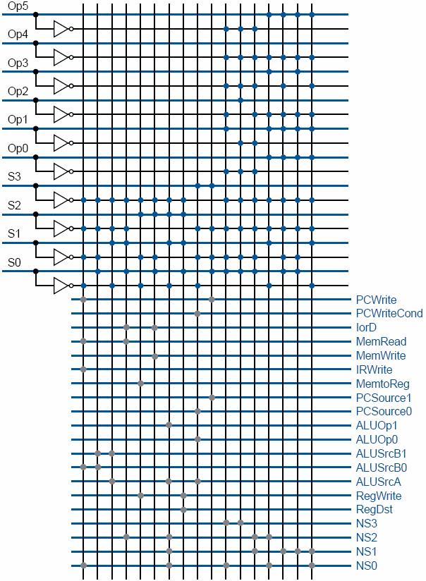
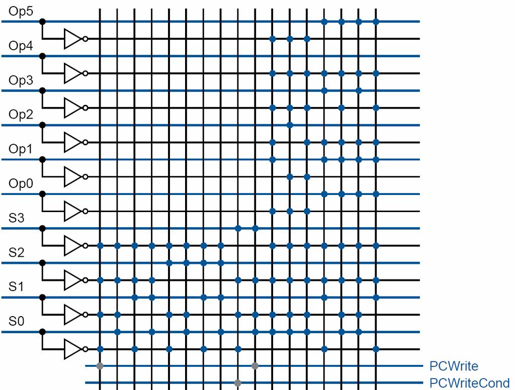
24 Control (Reading Assignment: Appendix C.2) Simple combinational logic (truth tables) Inputs Op5 Op4 ALUOp ALUOp0 ALUcontrol block Op3 Op2 Op1 Op0 ALUOp1 Outputs F (5 0) F3 F2 F1 F0 Operation2 Operation1 Operation0 Operation R-format Iw sw beq RegDst ALUSrc MemtoReg RegWrite MemRead MemWrite Branch ALUOp1 ALUOpO 24
25 Instruction RegDst ALUSrc R-format lw sw beq Memto- Reg Reg Write Mem Read Mem Write Branch ALUOp1 ALUp0 25
26 Datapath in Operation for R-Type Instruction Memto- Reg Mem Mem Instruction RegDst ALUSrc Reg Write Read Write Branch ALUOp1 ALUp0 R-format lw sw beq 26
27 Datapath in Operation for Load Instruction Memto- Reg Mem Mem Instruction RegDst ALUSrc Reg Write Read Write Branch ALUOp1 ALUp0 R-format lw sw X 1 X beq 27
28 Datapath in Operation for Branch Equal Instruction Memto- Reg Mem Mem Instruction RegDst ALUSrc Reg Write Read Write Branch ALUOp1 ALUp0 R-format lw sw X 1 X beq X 0 X
29 Datapath with control for Jump instruction J-type instructions use 6 bits for the opcode, and 26 bits for the immediate value (called the target). newpc <- PC[31-28] IR[25-0] 00 29
30 Timing: Single cycle implementation Calculate cycle time assuming negligible delays except Memory (2ns), ALU and adders (2ns), Register file access (1ns) 30
31 Why is Single Cycle not GOOD??? Memory - 2ns; ALU - 2ns; Adder - 2ns; Reg - 1ns Instruction class Instruction memory Register read ALU Data memory Register write Total (in ns) ALU type Load word Store word Branch Jump 2 2 what if we had floating point instructions to handle? 31
32 1 clock cycle fixed vs. variable for each instruction Memory - 2ns; ALU - 2ns; Adder - 2ns; Reg - 1ns Loads 24% Stores 12% R-type 44% Branch 18% Jumps 2% Instruction class Instruction memory Register read ALU Data memory Register write Total (in ns) ALU type Load word Store word Branch Jump
33 1 clock cycle fixed vs. variable for each instruction Memory - 2ns; ALU - 2ns; Adder - 2ns; Reg - 1ns Loads 24% Stores 12% R-type 44% Branch 18% Jumps 2% CPU = IC * CPI * CC CPU = 8*24% + 7*12% + 6*44% + 5*18% + 2*2% CPU = 6.3ns Instruction class Instruction memory Register read ALU Data memory Register write Total (in ns) ALU type Load word Store word Branch Jump
34 Single Cycle Problems Wasteful of area Each unit used once per clock cycle Clock cycle equal to worst case scenario Will reducing the delay of common case help? 34
35 Multicycle Approach Ability to allow different cycles for different instructions Ability to share functional units within the execution of a single instruction Each step in execution in 1 cycle Functional unit to be used more than once per instruction As long as it is used in different cycle This will lead to reduction in hardware 35
36 Where we are headed One Solution: use a smaller cycle time have different instructions take different numbers of cycles a multicycle datapath shares resources Break up the instructions into steps, each step takes a cycle balance the amount of work to be done restrict each cycle to use only one major functional unit At the end of a cycle store values for use in later cycles (easiest thing to do) introduce additional internal registers PC Address Instruction or data Memory Data Instruction register Memory data register Data Register # Registers Register # Register # A B ALU ALUOut What is new? One ALU Single memory Some registers 36
37 Multicycle Datapath R I op rs rt rd shamt funct op rs rt 16 bit address J op 26 bit address What is this wire for? 37
38 Multicycle Datapath with Control Signals Missing wires?? 38
39 Multicycle Datapath, All Together 39
40 Idea behind multicycle approach We define each instruction from the ISA perspective Break it down into steps following our rule that data flows through at most one major functional unit (e.g., balance work across steps) Introduce new registers as needed (e.g, A, B, ALUOut, MDR, etc.) Finally try and pack as much work into each step (avoid unnecessary cycles) while also trying to share steps where possible (minimizes control, helps to simplify solution) Result: Our book s multicycle Implementation! 40
41 Breaking down an instruction ISA definition of arithmetic: Reg[Memory[PC][15:11]] <= Reg[Memory[PC][25:21]] op Reg[Memory[PC][20:16]] Could break down to: IR <= Memory[PC] A <= Reg[IR[25:21]] B <= Reg[IR[20:16]] ALUOut <= A op B Reg[IR[20:16]] <= ALUOut We forgot an important part of the definition of arithmetic! PC <= PC
42 Five Execution Steps Instruction Fetch Instruction Decode and Register Fetch Execution, Memory Address Computation, or Branch Completion Memory Access or R-type instruction completion Write-back step INSTRUCTIONS TAKE FROM 3-5 CYCLES! 42
43 Step 1: Instruction Fetch Use PC to get instruction and put it in the Instruction Register. Increment the PC by 4 and put the result back in the PC. Can be described succinctly using RTL "Register-Transfer Language" IR <= Memory[PC]; PC <= PC + 4; Can we figure out the values of the control signals? What is the advantage of updating the PC now? 43
44 Step 2: Instruction Decode and Register Fetch Read registers rs and rt in case we need them Compute the branch address in case the instruction is a branch RTL: A <= Reg[IR[25:21]]; B <= Reg[IR[20:16]]; ALUOut <= PC + (sign-extend(ir[15:0]) << 2); We aren't setting any control lines based on the instruction type (we are busy "decoding" it in our control logic) 44
45 Step 3 Execution (instruction dependent) Memory Reference: ALUOut <= A + sign-extend(ir[15:0]); R-type: ALUOut <= A op B; Branch: if (A==B) PC <= ALUOut; Jump: PC <= {PC[31:28],(IR[25:0],2 b00)}; 45
46 Step 4 and 5 Step 4 R-type Completion or memory-access Memory access or R-type completion: MDR <= Memory[ALUout]; or Memory[ALUout] <= B; R-type instructions finish Reg[IR[15:11]] <= ALUOut; Step 5 Write-back step Reg[IR[20:16]] <= MDR; Why not do this in Step 4? 46

47 Summary: 47
48 Defining the Control Now that we have determined what the control signals are and when they have to be asserted Next step: implementing the control unit Single cycle datapath used truth tables Not feasible Alternatives Finite state machines Microprogramming 48
49 Implementing the Control Value of control signals is dependent upon: what instruction is being executed which step is being performed Use the information we ve accumulated to specify a finite state machine specify the finite state machine graphically, or use microprogramming Implementation can be derived from specification 49
50 Finite State Machine Control A <= Reg[IR[25:21]]; B <= Reg[IR[20:16]]; ALUOut <= PC + (sign-extend(ir[15:0]) << 2); IR <= Memory[PC]; PC <= PC + 4; 50
51 Big Picture 51
52 State Table 52
53 State Table 53
54 ROM Implementation ROM = "Read Only Memory" values of memory locations are fixed ahead of time A ROM can be used to implement a truth table if the address is m-bits, we can address 2 m entries in the ROM. our outputs are the bits of data that the address points to. m n m is the "height", and n is the "width" 54
55 ROM Implementation (Appendix-C!!!) How many inputs are there? 6 bits for opcode, 4 bits for state = 10 address lines (i.e., 2 10 = 1024 different addresses) How many outputs are there? 16 datapath-control outputs, 4 state bits = 20 outputs ROM is 2 10 x 20 = 20K bits (and a rather unusual size) Rather wasteful, since for lots of the entries, the outputs are the same i.e., opcode is often ignored 55
56 Big Picture 56


57 Putting All Together 57
58 PLA 58
59 59
60 ROM vs PLA Break up the table into two parts 4 state bits tell you the 16 outputs, 2 4 x 16 bits of ROM 10 bits tell you the 4 next state bits, 2 10 x 4 bits of ROM Total: 4.3K bits of ROM PLA is much smaller can share product terms only need entries that produce an active output can take into account don't cares Size is (#inputs #product-terms) + (#outputs #product-terms) For this example = (10x17)+(20x17) = 510 PLA cells PLA cells usually about the size of a ROM cell (slightly bigger) 60
61 Another Implementation Style Complex instructions: the "next state" is often current state + 1 Control unit PLA or ROM Input Outputs PCWrite PCWriteCond IorD MemRead MemWrite IRWrite BWrite MemtoReg PCSource ALUOp ALUSrcB ALUSrcA RegWrite RegDst AddrCtl 1 State Adder Address select logic Op[5 0] Instruction register opcode field 61
62 Microprogramming Control unit Microcode memory Input Outputs PCWrite PCWriteCond IorD MemRead MemWrite IRWrite BWrite MemtoReg PCSource ALUOp ALUSrcB ALUSrcA RegWrite RegDst AddrCtl Datapath 1 Microprogram counter Adder Address select logic Instruction register opcode field What are the microinstructions? 62

63 Pentium 4 Pipelining is important (last IA-32 without it was in 1985) Control Control I/O interface Instruction cache Enhanced floating point and multimedia Control Data cache Integer datapath Secondary cache and memory interface Chapter 7 Chapter 6 Advanced pipelining hyperthreading support Control Pipelining is used for the simple instructions favored by compilers Simply put, a high performance implementation needs to ensure that the simple instructions execute quickly, and that the burden of the complexities of the instruction set penalize the complex, less frequently used, instructions 63
64 Chapter 5 Summary If we understand the instructions We can build a simple processor! If instructions take different amounts of time, multi-cycle is better Datapath implemented using: Combinational logic for arithmetic State holding elements to remember bits Control implemented using: Combinational logic for single-cycle implementation Finite state machine for multi-cycle implementation 64
The Processor: Datapath & Control
 Chapter Five 1 The Processor: Datapath & Control We're ready to look at an implementation of the MIPS Simplified to contain only: memory-reference instructions: lw, sw arithmetic-logical instructions:
Lets Build a Processor
 Lets Build a Processor Almost ready to move into chapter 5 and start building a processor First, let s review Boolean Logic and build the ALU we ll need (Material from Appendix B) operation a 32 ALU result
Multicycle Approach. Designing MIPS Processor
 CSE 675.2: Introduction to Computer Architecture Multicycle Approach 8/8/25 Designing MIPS Processor (Multi-Cycle) Presentation H Slides by Gojko Babić and Elsevier Publishing We will be reusing functional
ﻪﺘﻓﺮﺸﻴﭘ ﺮﺗﻮﻴﭙﻣﺎﻛ يرﺎﻤﻌﻣ MIPS يرﺎﻤﻌﻣ data path and ontrol control
 معماري كامپيوتر پيشرفته معماري MIPS data path and control abbasi@basu.ac.ir Topics Building a datapath support a subset of the MIPS-I instruction-set A single cycle processor datapath all instruction actions
Chapter 4 The Processor (Part 2)
") Department of Electr rical Eng ineering, Chapter 4 The Processor (Part 2) 王振傑 (Chen-Chieh Wang) ccwang@mail.ee.ncku.edu.tw ncku edu Feng-Chia Unive ersity Outline A Multicycle Implementation Mapping Control
Department of Electr rical Eng ineering, Chapter 4 The Processor (Part 2) 王振傑 (Chen-Chieh Wang) ccwang@mail.ee.ncku.edu.tw ncku edu Feng-Chia Unive ersity Outline A Multicycle Implementation Mapping Control
Topic #6. Processor Design
 Topic #6 Processor Design Major Goals! To present the single-cycle implementation and to develop the student's understanding of combinational and clocked sequential circuits and the relationship between
ENE 334 Microprocessors
 ENE 334 Microprocessors Lecture 6: Datapath and Control : Dejwoot KHAWPARISUTH Adapted from Computer Organization and Design, 3 th & 4 th Edition, Patterson & Hennessy, 2005/2008, Elsevier (MK) http://webstaff.kmutt.ac.th/~dejwoot.kha/
Lecture 5 and 6. ICS 152 Computer Systems Architecture. Prof. Juan Luis Aragón
 ICS 152 Computer Systems Architecture Prof. Juan Luis Aragón Lecture 5 and 6 Multicycle Implementation Introduction to Microprogramming Readings: Sections 5.4 and 5.5 1 Review of Last Lecture We have seen
EECE 417 Computer Systems Architecture
 EECE 417 Computer Systems Architecture Department of Electrical and Computer Engineering Howard University Charles Kim Spring 2007 1 Computer Organization and Design (3 rd Ed) -The Hardware/Software Interface
Systems Architecture I
 Systems Architecture I Topics A Simple Implementation of MIPS * A Multicycle Implementation of MIPS ** *This lecture was derived from material in the text (sec. 5.1-5.3). **This lecture was derived from
CPE 335. Basic MIPS Architecture Part II
 CPE 335 Computer Organization Basic MIPS Architecture Part II Dr. Iyad Jafar Adapted from Dr. Gheith Abandah slides http://www.abandah.com/gheith/courses/cpe335_s08/index.html CPE232 Basic MIPS Architecture
Processor: Multi- Cycle Datapath & Control
 Processor: Multi- Cycle Datapath & Control (Based on text: David A. Patterson & John L. Hennessy, Computer Organization and Design: The Hardware/Software Interface, 3 rd Ed., Morgan Kaufmann, 27) COURSE
Chapter 5: The Processor: Datapath and Control
 Chapter 5: The Processor: Datapath and Control Overview Logic Design Conventions Building a Datapath and Control Unit Different Implementations of MIPS instruction set A simple implementation of a processor
CC 311- Computer Architecture. The Processor - Control
 CC 311- Computer Architecture The Processor - Control Control Unit Functions: Instruction code Control Unit Control Signals Select operations to be performed (ALU, read/write, etc.) Control data flow (multiplexor
LECTURE 6. Multi-Cycle Datapath and Control
 LECTURE 6 Multi-Cycle Datapath and Control SINGLE-CYCLE IMPLEMENTATION As we ve seen, single-cycle implementation, although easy to implement, could potentially be very inefficient. In single-cycle, we
CSE 2021 COMPUTER ORGANIZATION
 CSE 22 COMPUTER ORGANIZATION HUGH CHESSER CHESSER HUGH CSEB 2U 2U CSEB Agenda Topics:. Sample Exam/Quiz Q - Review 2. Multiple cycle implementation Patterson: Section 4.5 Reminder: Quiz #2 Next Wednesday
CSE 2021 COMPUTER ORGANIZATION
 CSE 2021 COMPUTER ORGANIZATION HUGH LAS CHESSER 1012U HUGH CHESSER CSEB 1012U W10-M Agenda Topics: 1. Multiple cycle implementation review 2. State Machine 3. Control Unit implementation for Multi-cycle
Implementing the Control. Simple Questions
 Simple Questions How many cycles will it take to execute this code? lw $t2, 0($t3) lw $t3, 4($t3) beq $t2, $t3, Label add $t5, $t2, $t3 sw $t5, 8($t3) Label:... #assume not What is going on during the
RISC Processor Design
 RISC Processor Design Single Cycle Implementation - MIPS Virendra Singh Indian Institute of Science Bangalore virendra@computer.org Lecture 13 SE-273: Processor Design Feb 07, 2011 SE-273@SERC 1 Courtesy:
Mapping Control to Hardware
 C A P P E N D I X A custom format such as this is slave to the architecture of the hardware and the instruction set it serves. The format must strike a proper compromise between ROM size, ROM-output decoding,
Lecture 8: Control COS / ELE 375. Computer Architecture and Organization. Princeton University Fall Prof. David August
 Lecture 8: Control COS / ELE 375 Computer Architecture and Organization Princeton University Fall 2015 Prof. David August 1 Datapath and Control Datapath The collection of state elements, computation elements,
Processor (I) - datapath & control. Hwansoo Han
 - datapath & control. Hwansoo Han") Processor (I) - datapath & control Hwansoo Han Introduction CPU performance factors Instruction count - Determined by ISA and compiler CPI and Cycle time - Determined by CPU hardware We will examine two
Processor (I) - datapath & control Hwansoo Han Introduction CPU performance factors Instruction count - Determined by ISA and compiler CPI and Cycle time - Determined by CPU hardware We will examine two
Lecture 5: The Processor
 Lecture 5: The Processor CSCE 26 Computer Organization Instructor: Saraju P. ohanty, Ph. D. NOTE: The figures, text etc included in slides are borrowed from various books, websites, authors pages, and
Multiple Cycle Data Path
 Multiple Cycle Data Path CS 365 Lecture 7 Prof. Yih Huang CS365 1 Multicycle Approach Break up the instructions into steps, each step takes a cycle balance the amount of work to be done restrict each cycle
Computer Science 324 Computer Architecture Mount Holyoke College Fall Topic Notes: Data Paths and Microprogramming
 Computer Science 324 Computer Architecture Mount Holyoke College Fall 2007 Topic Notes: Data Paths and Microprogramming We have spent time looking at the MIPS instruction set architecture and building
Inf2C - Computer Systems Lecture 12 Processor Design Multi-Cycle
 Inf2C - Computer Systems Lecture 12 Processor Design Multi-Cycle Boris Grot School of Informatics University of Edinburgh Previous lecture: single-cycle processor Inf2C Computer Systems - 2017-2018. Boris
Alternative to single cycle. Drawbacks of single cycle implementation. Multiple cycle implementation. Instruction fetch
 Drawbacks of single cycle implementation Alternative to single cycle All instructions take the same time although some instructions are longer than others; e.g. load is longer than add since it has to
Major CPU Design Steps
 Datapath Major CPU Design Steps. Analyze instruction set operations using independent RTN ISA => RTN => datapath requirements. This provides the the required datapath components and how they are connected
RISC Architecture: Multi-Cycle Implementation
 RISC Architecture: Multi-Cycle Implementation Virendra Singh Associate Professor Computer Architecture and Dependable Systems Lab Department of Electrical Engineering Indian Institute of Technology Bombay
Points available Your marks Total 100
 CSSE 3 Computer Architecture I Rose-Hulman Institute of Technology Computer Science and Software Engineering Department Exam Name: Section: 3 This exam is closed book. You are allowed to use the reference
CS/COE0447: Computer Organization
 CS/COE0447: Computer Organization and Assembly Language Datapath and Control Sangyeun Cho Dept. of Computer Science A simple MIPS We will design a simple MIPS processor that supports a small instruction
CS/COE0447: Computer Organization
 A simple MIPS CS/COE447: Computer Organization and Assembly Language Datapath and Control Sangyeun Cho Dept. of Computer Science We will design a simple MIPS processor that supports a small instruction
Design of the MIPS Processor
 Design of the MIPS Processor We will study the design of a simple version of MIPS that can support the following instructions: I-type instructions LW, SW R-type instructions, like ADD, SUB Conditional
Computer Science 141 Computing Hardware
 Computer Science 4 Computing Hardware Fall 6 Harvard University Instructor: Prof. David Brooks dbrooks@eecs.harvard.edu Upcoming topics Mon, Nov th MIPS Basic Architecture (Part ) Wed, Nov th Basic Computer
Chapter 5 Solutions: For More Practice
 Chapter 5 Solutions: For More Practice 1 Chapter 5 Solutions: For More Practice 5.4 Fetching, reading registers, and writing the destination register takes a total of 300ps for both floating point add/subtract
ELEC 5200/6200 Computer Architecture and Design Spring 2017 Lecture 4: Datapath and Control
 ELEC 52/62 Computer Architecture and Design Spring 217 Lecture 4: Datapath and Control Ujjwal Guin, Assistant Professor Department of Electrical and Computer Engineering Auburn University, Auburn, AL 36849
Processor (multi-cycle)
") CS359: Computer Architecture Processor (multi-cycle) Yanyan Shen Department of Computer Science and Engineering Five Instruction Steps ) Instruction Fetch ) Instruction Decode and Register Fetch 3) R-type
CS359: Computer Architecture Processor (multi-cycle) Yanyan Shen Department of Computer Science and Engineering Five Instruction Steps ) Instruction Fetch ) Instruction Decode and Register Fetch 3) R-type
Systems Architecture
 Systems Architecture Lecture 15: A Simple Implementation of MIPS Jeremy R. Johnson Anatole D. Ruslanov William M. Mongan Some or all figures from Computer Organization and Design: The Hardware/Software
CO Computer Architecture and Programming Languages CAPL. Lecture 18 & 19
 CO2-3224 Computer Architecture and Programming Languages CAPL Lecture 8 & 9 Dr. Kinga Lipskoch Fall 27 Single Cycle Disadvantages & Advantages Uses the clock cycle inefficiently the clock cycle must be
RISC Architecture: Multi-Cycle Implementation
 RISC Architecture: Multi-Cycle Implementation Virendra Singh Associate Professor Computer Architecture and Dependable Systems Lab Department of Electrical Engineering Indian Institute of Technology Bombay
Design of the MIPS Processor (contd)
") Design of the MIPS Processor (contd) First, revisit the datapath for add, sub, lw, sw. We will augment it to accommodate the beq and j instructions. Execution of branch instructions beq $at, $zero, L add
Design of the MIPS Processor (contd) First, revisit the datapath for add, sub, lw, sw. We will augment it to accommodate the beq and j instructions. Execution of branch instructions beq $at, $zero, L add
ALUOut. Registers A. I + D Memory IR. combinatorial block. combinatorial block. combinatorial block MDR
 Microprogramming Exceptions and interrupts 9 CMPE Fall 26 A. Di Blas Fall 26 CMPE CPU Multicycle From single-cycle to Multicycle CPU with sequential control: Finite State Machine Textbook Edition: 5.4,
ECE 313 Computer Organization FINAL EXAM December 14, This exam is open book and open notes. You have 2 hours.
 This exam is open book and open notes. You have 2 hours. Problems 1-4 refer to a proposed MIPS instruction lwu (load word - update) which implements update addressing an addressing mode that is used in
Chapter 4. The Processor. Computer Architecture and IC Design Lab
 Chapter 4 The Processor Introduction CPU performance factors CPI Clock Cycle Time Instruction count Determined by ISA and compiler CPI and Cycle time Determined by CPU hardware We will examine two MIPS
RISC Design: Multi-Cycle Implementation
 RISC Design: Multi-Cycle Implementation Virendra Singh Associate Professor Computer Architecture and Dependable Systems Lab Department of Electrical Engineering Indian Institute of Technology Bombay http://www.ee.iitb.ac.in/~viren/
Microprogramming. Microprogramming
 Microprogramming Alternative way of specifying control FSM State -- bubble control signals in bubble next state given by signals on arc not a great language to specify when things are complex Treat as
COMPUTER ORGANIZATION AND DESIGN. The Hardware/Software Interface. Chapter 4. The Processor: A Based on P&H
 COMPUTER ORGANIZATION AND DESIGN The Hardware/Software Interface Chapter 4 The Processor: A Based on P&H Introduction We will examine two MIPS implementations A simplified version A more realistic pipelined
Multicycle conclusion
 Multicycle conclusion The last few lectures covered a lot of material! We introduced a multicycle datapath, where different instructions take different numbers of cycles to execute. A multicycle unit is
TDT4255 Computer Design. Lecture 4. Magnus Jahre. TDT4255 Computer Design
 1 TDT4255 Computer Design Lecture 4 Magnus Jahre 2 Outline Chapter 4.1 to 4.4 A Multi-cycle Processor Appendix D 3 Chapter 4 The Processor Acknowledgement: Slides are adapted from Morgan Kaufmann companion
Note- E~ S. \3 \S U\e. ~ ~s ~. 4. \\ o~ (fw' \i<.t. (~e., 3\0)
") 5.4 A Multicycle Implementation 377 Similarly, if we had a machine with more powerful operations and addressing modes, instructions could vary from three or four functional unit delays to tens or even
5.4 A Multicycle Implementation 377 Similarly, if we had a machine with more powerful operations and addressing modes, instructions could vary from three or four functional unit delays to tens or even
Computer Organization and Structure. Bing-Yu Chen National Taiwan University
 Computer Organization and Structure Bing-Yu Chen National Taiwan University The Processor Logic Design Conventions Building a Datapath A Simple Implementation Scheme An Overview of Pipelining Pipelined
Single vs. Multi-cycle Implementation
 Single vs. Multi-cycle Implementation Multicycle: Instructions take several faster cycles For this simple version, the multi-cycle implementation could be as much as 1.27 times faster (for a typical instruction
Using a Hardware Description Language to Design and Simulate a Processor 5.8
 5.8 Using a Hardware Description Language to Design and Simulate a Processor 5.8 As mentioned in Appix B, Verilog can describe processors for simulation or with the intention that the Verilog specification
Initial Representation Finite State Diagram. Logic Representation Logic Equations
 Control Implementation Alternatives Control may be designed using one of several initial representations. The choice of sequence control, and how logic is represented, can then be determined independently;
Single Cycle Datapath
 Single Cycle atapath Lecture notes from MKP, H. H. Lee and S. Yalamanchili Section 4.1-4.4 Appendices B.3, B.7, B.8, B.11,.2 ing Note: Appendices A-E in the hardcopy text correspond to chapters 7-11 in
THE HONG KONG UNIVERSITY OF SCIENCE & TECHNOLOGY Computer Organization (COMP 2611) Spring Semester, 2014 Final Examination
 Spring Semester, 2014 Final Examination") THE HONG KONG UNIVERSITY OF SCIENCE & TECHNOLOGY Computer Organization (COMP 2611) Spring Semester, 2014 Final Examination May 23, 2014 Name: Email: Student ID: Lab Section Number: Instructions: 1. This
THE HONG KONG UNIVERSITY OF SCIENCE & TECHNOLOGY Computer Organization (COMP 2611) Spring Semester, 2014 Final Examination May 23, 2014 Name: Email: Student ID: Lab Section Number: Instructions: 1. This
ECE232: Hardware Organization and Design
 ECE232: Hardware Organization and Design Lecture 14: One Cycle MIPs Datapath Adapted from Computer Organization and Design, Patterson & Hennessy, UCB R-Format Instructions Read two register operands Perform
Control Unit for Multiple Cycle Implementation
 Control Unit for Multiple Cycle Implementation Control is more complex than in single cycle since: Need to define control signals for each step Need to know which step we are on Two methods for designing
Control & Execution. Finite State Machines for Control. MIPS Execution. Comp 411. L14 Control & Execution 1
 Control & Execution Finite State Machines for Control MIPS Execution L14 Control & Execution 1 Synchronous Systems data Latch Combinational logic Latch Clock leading edge trailing edge On the leading edge
CPU Organization (Design)
") ISA Requirements CPU Organization (Design) Datapath Design: Capabilities & performance characteristics of principal Functional Units (FUs) needed by ISA instructions (e.g., Registers, ALU, Shifters, Logic
ISA Requirements CPU Organization (Design) Datapath Design: Capabilities & performance characteristics of principal Functional Units (FUs) needed by ISA instructions (e.g., Registers, ALU, Shifters, Logic
COMP303 - Computer Architecture Lecture 8. Designing a Single Cycle Datapath
 COMP33 - Computer Architecture Lecture 8 Designing a Single Cycle Datapath The Big Picture The Five Classic Components of a Computer Processor Input Control Memory Datapath Output The Big Picture: The
Processor Implementation in VHDL. University of Ulster at Jordanstown University of Applied Sciences, Augsburg
 University of Ulster at Jordanstown University of Applied Sciences, Augsburg Master of Engineering VLSI Design Project Report Processor Implementation in VHDL According to Computer Organisation & Design
ECE 3056: Architecture, Concurrency and Energy of Computation. Single and Multi-Cycle Datapaths: Practice Problems
 ECE 3056: Architecture, Concurrency and Energy of Computation Single and Multi-Cycle Datapaths: Practice Problems 1. Consider the single cycle SPIM datapath. a. Specify the values of the control signals
Chapter 4. The Processor
 Chapter 4 The Processor Introduction CPU performance factors Instruction count Determined by ISA and compiler CPI and Cycle time Determined by CPU hardware We will examine two MIPS implementations A simplified
Outline. Combinational Element. State (Sequential) Element. Clocking Methodology. Input/Output of Elements
 Element. Clocking Methodology. Input/Output of Elements") Outline ombinational Element ombinational & sequential logic Single-cycle PU ulti-cycle PU Examples of ombinational Elements State (Sequential) Element! "#$$$ #$$ #$$ #$ # & & ) *.// * - + #3, * + - locking
Outline ombinational Element ombinational & sequential logic Single-cycle PU ulti-cycle PU Examples of ombinational Elements State (Sequential) Element! "#$$$ #$$ #$$ #$ # & & ) *.// * - + #3, * + - locking
CENG 3420 Computer Organization and Design. Lecture 06: MIPS Processor - I. Bei Yu
 CENG 342 Computer Organization and Design Lecture 6: MIPS Processor - I Bei Yu CEG342 L6. Spring 26 The Processor: Datapath & Control q We're ready to look at an implementation of the MIPS q Simplified
The Processor (1) Jinkyu Jeong Computer Systems Laboratory Sungkyunkwan University
 Jinkyu Jeong Computer Systems Laboratory Sungkyunkwan University") The Processor (1) Jinkyu Jeong (jinkyu@skku.edu) Computer Systems Laboratory Sungkyunkwan University http://csl.skku.edu EEE3050: Theory on Computer Architectures, Spring 2017, Jinkyu Jeong (jinkyu@skku.edu)
The Processor (1) Jinkyu Jeong (jinkyu@skku.edu) Computer Systems Laboratory Sungkyunkwan University http://csl.skku.edu EEE3050: Theory on Computer Architectures, Spring 2017, Jinkyu Jeong (jinkyu@skku.edu)
Chapter 4. The Processor
 Chapter 4 The Processor Introduction CPU performance factors Instruction count Determined by ISA and compiler CPI and Cycle time Determined by CPU hardware 4.1 Introduction We will examine two MIPS implementations
CSE 2021: Computer Organization Fall 2010 Solution to Assignment # 3: Multicycle Implementation
 CSE 2021: Computer Organization Fall 2010 Solution to Assignment # 3: Multicycle Implementation Note that these questions are taken from the previous final exmas of CSE2021 and should serve as practice
The Processor. Z. Jerry Shi Department of Computer Science and Engineering University of Connecticut. CSE3666: Introduction to Computer Architecture
 The Processor Z. Jerry Shi Department of Computer Science and Engineering University of Connecticut CSE3666: Introduction to Computer Architecture Introduction CPU performance factors Instruction count
Multi-cycle Approach. Single cycle CPU. Multi-cycle CPU. Requires state elements to hold intermediate values. one clock cycle or instruction
 Multi-cycle Approach Single cycle CPU State element Combinational logic State element clock one clock cycle or instruction Multi-cycle CPU Requires state elements to hold intermediate values State Element
The Processor: Datapath and Control. Jin-Soo Kim Computer Systems Laboratory Sungkyunkwan University
 The Processor: Datapath and Control Jin-Soo Kim (jinsookim@skku.edu) Computer Systems Laboratory Sungkyunkwan University http://csl.skku.edu Introduction CPU performance factors Instruction count Determined
Digital Design & Computer Architecture (E85) D. Money Harris Fall 2007
 D. Money Harris Fall 2007") Digital Design & Computer Architecture (E85) D. Money Harris Fall 2007 Final Exam This is a closed-book take-home exam. You are permitted a calculator and two 8.5x sheets of paper with notes. The exam
Digital Design & Computer Architecture (E85) D. Money Harris Fall 2007 Final Exam This is a closed-book take-home exam. You are permitted a calculator and two 8.5x sheets of paper with notes. The exam
CS232 Final Exam May 5, 2001
 CS232 Final Exam May 5, 2 Name: This exam has 4 pages, including this cover. There are six questions, worth a total of 5 points. You have 3 hours. Budget your time! Write clearly and show your work. State
4. What is the average CPI of a 1.4 GHz machine that executes 12.5 million instructions in 12 seconds?
 Chapter 4: Assessing and Understanding Performance 1. Define response (execution) time. 2. Define throughput. 3. Describe why using the clock rate of a processor is a bad way to measure performance. Provide
Computer Architecture Chapter 5. Fall 2005 Department of Computer Science Kent State University
 Compter Architectre Chapter 5 Fall 25 Department of Compter Science Kent State University The Processor: Datapath & Control Or implementation of the MIPS is simplified memory-reference instrctions: lw,
ECE260: Fundamentals of Computer Engineering
 Datapath for a Simplified Processor James Moscola Dept. of Engineering & Computer Science York College of Pennsylvania Based on Computer Organization and Design, 5th Edition by Patterson & Hennessy Introduction
COMPUTER ORGANIZATION AND DESIGN. 5 th Edition. The Hardware/Software Interface. Chapter 4. The Processor
 COMPUTER ORGANIZATION AND DESIGN The Hardware/Software Interface 5 th Edition Chapter 4 The Processor Introduction CPU performance factors Instruction count Determined by ISA and compiler CPI and Cycle
Inf2C - Computer Systems Lecture Processor Design Single Cycle
 Inf2C - Computer Systems Lecture 10-11 Processor Design Single Cycle Boris Grot School of Informatics University of Edinburgh Previous lectures Combinational circuits Combinations of gates (INV, AND, OR,
Chapter 4. Instruction Execution. Introduction. CPU Overview. Multiplexers. Chapter 4 The Processor 1. The Processor.
 COMPUTER ORGANIZATION AND DESIGN The Hardware/Software Interface 5 th Edition COMPUTER ORGANIZATION AND DESIGN The Hardware/Software Interface 5 th Edition Chapter 4 The Processor The Processor - Introduction
COMPUTER ORGANIZATION AND DESIGN. 5 th Edition. The Hardware/Software Interface. Chapter 4. The Processor
 COMPUTER ORGANIZATION AND DESIGN The Hardware/Software Interface 5 th Edition Chapter 4 The Processor COMPUTER ORGANIZATION AND DESIGN The Hardware/Software Interface 5 th Edition The Processor - Introduction
LECTURE 5. Single-Cycle Datapath and Control
 LECTURE 5 Single-Cycle Datapath and Control PROCESSORS In lecture 1, we reminded ourselves that the datapath and control are the two components that come together to be collectively known as the processor.
Single Cycle Datapath
 Single Cycle atapath Lecture notes from MKP, H. H. Lee and S. Yalamanchili Section 4.-4.4 Appendices B.7, B.8, B.,.2 Practice Problems:, 4, 6, 9 ing (2) Introduction We will examine two MIPS implementations
EECS150 - Digital Design Lecture 10- CPU Microarchitecture. Processor Microarchitecture Introduction
 EECS150 - Digital Design Lecture 10- CPU Microarchitecture Feb 18, 2010 John Wawrzynek Spring 2010 EECS150 - Lec10-cpu Page 1 Processor Microarchitecture Introduction Microarchitecture: how to implement
Chapter 4. The Processor. Instruction count Determined by ISA and compiler. We will examine two MIPS implementations
 Chapter 4 The Processor Part I Introduction CPU performance factors Instruction count Determined by ISA and compiler CPI and Cycle time Determined by CPU hardware We will examine two MIPS implementations
Computer Organization & Design The Hardware/Software Interface Chapter 5 The processor : Datapath and control
 Computer Organization & Design The Hardware/Software Interface Chapter 5 The processor : Datapath and control Qing-song Shi http://.24.26.3 Email: zjsqs@zju.edu.cn Chapter 5 The processor : Datapath and
Computer and Information Sciences College / Computer Science Department Enhancing Performance with Pipelining
 Computer and Information Sciences College / Computer Science Department Enhancing Performance with Pipelining Single-Cycle Design Problems Assuming fixed-period clock every instruction datapath uses one
CPE 335 Computer Organization. Basic MIPS Architecture Part I
 CPE 335 Computer Organization Basic MIPS Architecture Part I Dr. Iyad Jafar Adapted from Dr. Gheith Abandah slides http://www.abandah.com/gheith/courses/cpe335_s8/index.html CPE232 Basic MIPS Architecture
Lecture 4: Review of MIPS. Instruction formats, impl. of control and datapath, pipelined impl.
 Lecture 4: Review of MIPS Instruction formats, impl. of control and datapath, pipelined impl. 1 MIPS Instruction Types Data transfer: Load and store Integer arithmetic/logic Floating point arithmetic Control
CSE 2021 Computer Organization. Hugh Chesser, CSEB 1012U W10-M
 CSE 22 Computer Organization Hugh Chesser, CSEB 2U Agenda Topics:. ultiple cycle implementation - complete Patterson: Appendix C, D 2 Breaking the Execution into Clock Cycles Execution of each instruction
The MIPS Processor Datapath
 The MIPS Processor Datapath Module Outline MIPS datapath implementation Register File, Instruction memory, Data memory Instruction interpretation and execution. Combinational control Assignment: Datapath
EECS150 - Digital Design Lecture 9- CPU Microarchitecture. Watson: Jeopardy-playing Computer
 EECS150 - Digital Design Lecture 9- CPU Microarchitecture Feb 15, 2011 John Wawrzynek Spring 2011 EECS150 - Lec09-cpu Page 1 Watson: Jeopardy-playing Computer Watson is made up of a cluster of ninety IBM
Single Cycle Data Path
 Single ycle ata Path S 365 Lecture 6 Prof. Yih Huang S365 1 MIPS Lite We're ready to look at an implementation of the MIPS Simplified to support only: memory-reference instructions: lw, sw arithmetic-logical
Announcements. This week: no lab, no quiz, just midterm
 CSC258 Week 7 Announcements This week: no lab, no quiz, just midterm 2 Recap ALU Multiplication 3 To implement multiplication, we basically repeatedly do three things AND (one-bit multiplication) Addition
CS Computer Architecture Spring Week 10: Chapter
 CS 35101 Computer Architecture Spring 2008 Week 10: Chapter 5.1-5.3 Materials adapated from Mary Jane Irwin (www.cse.psu.edu/~mji) and Kevin Schaffer [adapted from D. Patterson slides] CS 35101 Ch 5.1
CSE Computer Architecture I Fall 2009 Lecture 13 In Class Notes and Problems October 6, 2009
 CSE 30321 Computer Architecture I Fall 2009 Lecture 13 In Class Notes and Problems October 6, 2009 Question 1: First, we briefly review the notion of a clock cycle (CC). Generally speaking a CC is the
Review: Abstract Implementation View
 Review: Abstract Implementation View Split memory (Harvard) model - single cycle operation Simplified to contain only the instructions: memory-reference instructions: lw, sw arithmetic-logical instructions:
Chapter 4. The Processor Designing the datapath
 Chapter 4 The Processor Designing the datapath Introduction CPU performance determined by Instruction Count Clock Cycles per Instruction (CPI) and Cycle time Determined by Instruction Set Architecure (ISA)
CENG 3420 Lecture 06: Datapath
 CENG 342 Lecture 6: Datapath Bei Yu byu@cse.cuhk.edu.hk CENG342 L6. Spring 27 The Processor: Datapath & Control q We're ready to look at an implementation of the MIPS q Simplified to contain only: memory-reference
Initial Representation Finite State Diagram Microprogram. Sequencing Control Explicit Next State Microprogram counter
 Control Implementation Alternatives Control may be designed using one of several initial representations. The choice of sequence control, and how logic is represented, can then be determined independently;