Near-Field Coupling Integration Technology
|
|
|
- Gerard Lindsey
- 6 years ago
- Views:
Transcription


1 Near-Field Coupling Integration Technology 128-Die Stacking ISSCC2010, pp Tadahiro Kuroda Keio University, Japan IEEE Fellow August 31, of 40


2 Challenge to Tyranny of Numbers From System on a Chip to System on Chips ENIAC thousand vacuum tubes, 5 million hand-soldered connections Cray Mass of wires, cables, and connectors K thousand cables, 1,000Km long IEEE Spectrum Invention of transistor (1948), IC (1958) End of Moore s Law Invention of IC driven by Tyranny of Numbers : Challenges implied by large number of components & interconnects. We face the same challenge again with end of Moore s Law and rise of IoT/big data. 2of 40


 Cross section")

 Smart cards")
3 Proposal: Near-Field Coupling Replace mechanical connections (wires, solders, connectors) by electrical ones (wireless by near-field coupling). Near-field coupling provides with invisible wires. Near Field (Reactive) Cross section Top view (dotted circles: coils) Near Field : x< /2 x: distance, : wave length V RX 1/x 3 (-60dB/dec) Far Field (Radiative) Smart cards used in place of train ticket, door key WiFi, Cellular 3of 40

 Processor boards")
:")
 Proof of Concept: 100GFLOPS/W (in 2019) Milestone: 512GB/s")
4 Near-Field Coupling Integration Technology Proposed solution to connections in very large system H SoC chips ThruChip Interface (TCI) 3D integration of chips for high performance Memory chips H E Peripheral boards (storage and sensor) Processor boards Transmission Line Coupler (TLC) LEGO-type packaging of modules for high function 100GFLOPS/W 512GB/s JST ACCEL Project ( ): Data Centric Computer (Ultra low power mobile computer in the era of IoT) Proof of Concept: 100GFLOPS/W (in 2019) Milestone: 512GB/s 8GB DRAM (in 2017) 4of 40
5 Outline Near-Field Coupling Integration Technology Transmission Line Coupler (TLC) ThruChip Interface (TCI) Challenges Highly Doped Silicon Vias (HDSV) TCI_2.9D/2.5D/2.0D ACCEL 100GFLOPS/W Computer and 512GB/s DRAM 5of 40
")
6 Transmission Line Coupler (TLC) TL Crosstalk TL PCB, FPC Coupling PCB, FPC PCB, FPC Termination Magnetic Field Electric Field Transmission Line Coupler (TLC) 6of 40

7 Transmission Line Coupler (TLC) L H W E d distributed system ISSCC2011, pp Electromagnetic coupling characteristic impedance is controlled signal reflection can be suppressed Transceiver: digital CMOS circuits Contactless connector Modular design Coupling [db] Bandwidth : 8GHz (L=6mm), 12GHz (L=4mm) Distance (d): 1mm (W=0.5mm), 2mm (W=1mm) Frequency [GHz] Video 1 Video 2 7of 40
8 Applications of TLC SD LCD Memory Card High-speed:50x(12Gb/s) Low-power:1/500 Water proof (pad-less, sealed) ISSCC2013, pp Display High-speed:10x(6Gb/s) Low-energy:1/10(16pJ/b) Thin (no mechanical structure) ISSCC2013, pp Smartphone High-speed :5x(6Gb/s) Low-energy :1/24(6pJ/b) Modular design (electrical connection) ISSCC2015, pp ECU ECU ECU DIMM High speed:5x(12.5gb/s) Multi-drop bus (impedance controlled) ISSCC2012, pp In-vehicle LAN Light: 30% Strong EMC immunity (wide band) ISSCC2014, pp Satellite Light: 60% Vibration immunity (contactless connection) ISSCC2015, pp of 40

9 Display/Camera Module High speed, Low power, Low profile ISSCC2013, pp of 40


10 Modular Design 6Gb/s received data Module TLC 1.5mm 4mm TLC Module board Host board 5mm TLC LCD Module board ISSCC2015, pp Video of 40


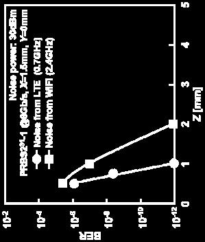
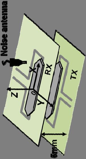

11 Radiation Tolerance (EMC) 1) EMI: Electromagnetic Interference GPS is not affected at a separation of 10mm from TLC Robot arm EM probe T-TLC 2) EMS: Electromagnetic Susceptibility TLC is not affected at a separation of 2mm from LTE/WiFi 11 of 40

![bits during 60 seconds 10-11 0 4 8 12 16 20 Vibration [G rms ] No single bit](/docs-images/78/77621936/images/12-1.jpg "failure during the period of launch of small locket ISSCC2015, pp.")
12 Vibration Tolerance Japan Aerospace exploration Agency Conventional mechanical connector TLC 10-3 TLC 1/246x PRBS BER No error bits during 60 seconds Vibration [G rms ] No single bit failure during the period of launch of small locket ISSCC2015, pp of 40

13 Other Possibilities In Slide (1D) Out In Rotate (2D) Rotate (3D) Out door, seat wheel, joint Module 1 Module 2 Video 4 DC isolation Touch and Go Hot swap 13 of 40
14 Outline Near-Field Coupling Integration Technology Transmission Line Coupler (TLC) ThruChip Interface (TCI) Challenges Highly Doped Silicon Vias (HDSV) TCI_2.9D/2.5D/2.0D ACCEL 100GFLOPS/W Computer and 512GB/s DRAM 14 of 40

 Digital CMOS circuit solution")
15 ThruChip Interface (TCI) V R =k L T L R I T di T dt S =1 Inductive coupling data communication through chips Transceiver: digital CMOS circuits Txdata Txdata Txdata I T ISSCC2004, pp Tx 15m x 10m 20m x 10m Rx 65nm CMOS Rxdata Rxdata Time Coil: multi-layer standard wires Logic interconnections go across coil Coil can be placed anywhere (above SRAM) Digital CMOS circuit solution Eventually zero cost V R Rxdata 15 of 40

 (1000ch in 2.")

 ISSCC2007 0.")


16 Performance of TCI High Speed Low Power 11Gb/s/ch (0.18m) ISSCC Gb/s/ch 8Tb/s (65nm) (1000ch in 2.5mm 2 ) A-SSCC2010 ISSCC2010 Aggregated data rate is raised by increasing number of channels. 0.14pJ/b (90nm) ISSCC pJ/b (65nm) JSSC2011 ESD protection device (>0.5pJ/b) can be eliminated. High Integration Low Height Low Thermal Resistance Bump 64-die stacking ISSCC die stacking ISSCC2010 TCI TSV 16 of 40
17 TCI Coil Design Data rate goes up dramatically with smaller Z Usable Coil bandwidth [Gb/s] Usable circuit bandwidth depends on device Gbps Z=20m D=100m D=200m 3-die stacking D=60m Usable BW of 22 Gbps Z=80m Coil Diameter D = Z distance x 3 9 die stacking D=240m D=300m D=400m D=500m Communication Distance, Z [m] 17 of 40

18 TCI Layout Similar to typical CMOS layout Coils of 100um size are formed by M9 and M10 for TX, M7 and M8 for RX, with power/signal lines crossing Accommodate circuits under the coil Coils are overlapped and accessed by PDMA to avoid crosstalk at phase 1 at phase 2 at phase 3 at phase 4 18 of 40
19 TSV vs. TCI TSV KOZ ** transistor micro bump TCI Magnetic Field transistor Solution Mechanical in package Electrical on wafer Wafer Technology Package Technology Miniaturization Yield Eco-system Additional Cost Placement Speed ESD Protection Power Dissipation Additional steps needed OSAT * involved Difficult Low, difficult to improve New model needed > 40% Dedicated area w/koz** < 512 GB/s Needed High Standard CMOS Conventional Easy High (~100%) Conventional model A few % Unconstrained > 512 GB/s No need Low OSAT * : Outsource Assembly and Test, KOZ **: Keep Out Zone 19 of 40
 Size:1/2x Voltage:1/2x Speed:2x Power/Area:1x evaluation value dimension scaling Device size [x] 1/ Voltage [V] 1/ Current [I] 1/ Capacitance [C]~[xx/x] 1/ Delay")
![time [t]~[cv/i] 1/ Constant Electric Field Scaling Inductive Coupling Link (3D Scaling Law) Thickness:1/2x Data Rate/Area:8x Energy/bit:1/8x Chip thickness [z] 1/ Coil size [D] 1/ Coil turn number](/docs-images/78/77621936/images/20-1.jpg "[n] 0.8 Inductance [L]~[n 2 D 1.")
20 3D Scaling Scenario Cost/Performance will be improved by 3D scaling scenario. Field Effect Transistor (Moore s Law) Size:1/2x Voltage:1/2x Speed:2x Power/Area:1x evaluation value dimension scaling Device size [x] 1/ Voltage [V] 1/ Current [I] 1/ Capacitance [C]~[xx/x] 1/ Delay time [t]~[cv/i] 1/ Constant Electric Field Scaling Inductive Coupling Link (3D Scaling Law) Thickness:1/2x Data Rate/Area:8x Energy/bit:1/8x Chip thickness [z] 1/ Coil size [D] 1/ Coil turn number [n] 0.8 Inductance [L]~[n 2 D 1.6 ] Magnetic coupling [k]~[z/d] Received signal [v R ]~[kl(i/t)] Data rate / channel [1/t] Channel / area [1/D 2 ] 2 Constant Magnetic Field Scaling Data rate / area [1/tD 2 ] 2 Energy / bit [IVt] 1/ 3 Suppose 8mm-square 4 chips are stacked. When each die is thinned from 50um to 10um, number of on-chip coils are increased from 700 to 17,500, yielding 25x speed improvement. 20 of 40
21 Performance of TCI in 7nm CMOS Chip thickness 50 m 25 m Coil size 150 m 75 m Data rate per coil 50 Gb/s/coil 64 Gb/s/coil Area efficiency 2 Tb/s/mm 2 11 Tb/s/mm 2 Power efficiency 30 fj/bit 25 fj/bit Aggregate data rate when using 8mm x 1mm Si area Power dissipation when using 8mm x 1mm Si area 18 Tb/s 91 Tb/s 0.5 W 2.2 W SPICE simulation performed with Predictive Technology Model ( 21 of 40
22 3-D NoC by TCI JSPS project led by Prof. Amano, Prof. Matsutani A Study on Building-Block Computing Systems using TCI Inter-chip wireless inductive coupling techniques, selforganized network-on-chips, fault tolerant architectures, optimized power control, and a flexible operating system with virtualization facilities are investigated 3-D NoC with TCI will be presented at IEEE A-SSCC2016 Collision detection scheme by sensing magnetic field 44-bit packet transceiver of PER < of 40
23 Outline Near-Field Coupling Integration Technology Transmission Line Coupler (TLC) ThruChip Interface (TCI) Challenges Highly Doped Silicon Vias (HDSV) TCI_2.9D/2.5D/2.0D ACCEL 100GFLOPS/W Computer and 512GB/s DRAM 23 of 40
24 Remaining Challenges Proof with DRAM Influence of magnetic field to DRAM Influence of DRAM (plate, cylinder, power mesh) to magnetic field Power Supply New way of power delivery to create synergy with TCI is expected. Highly Doped Silicon Vias (HDSV) is proposed. Idea is received highly in IEDM but needs proof. Heat Removal Heat keeps from die stacking. Inductive coupling for horizontal link (TCI_2.5D/2D) is developed. 24 of 40


25 Highly Doped Silicon Vias (HDSV) IEDM2014, A deeper and more highly doped well is used to make a low resistance HDSV. The HDSV on one die and electrodes on the next die are connected by pressure from a Room-Temperature Wafer Level Bonding machine to create larger stacks. TCAD indicates resistance < 3m when substrate <5um, dose: 1x10 16 cm -2, implant: 200 kev, annealing: 50h, 1050 C. 0.7 mm 2 net area is required (can be divided), good only for power delivery. Low cost process by implants 25 of 40
26 Memory Stacking with TCI and HDSV NAND Stacking wire bond TCI, HDSV ~1000 m spacer ~80 m ~275 m DRAM Stacking TSV TCI, HDSV DRAM die DRAM die DRAM die DRAM die ~40 m Base logic die # stacked die Die pitch Total height Die area Data link Power delivery IO energy/bit IO data rate/area ~1000 1x wire bond wire bond 1x 16 5 ~80 ~0.9x TCI HDSV < 1/400x 5 55 ~275 1x TSV TSV 1x ~ 200 Gb/s/mm ~40 ~0.9x TCI HDSV < 1/10x ~ 860 Gb/s/mm 2 Hot Chips of 40

 0.250 mm CLK 1 CLK 3 TCI, HDSV 6.")

27 128GB/s HBM Case Study 5.1 mm TCI reduced chip size by 13% than TSV. TSV 6.91 mm SK Hynix, ISSCC2014 1Gb/s/TSV*1024 TSV=128 GB/s 2.5 coils 250 TSV (dedicated) mm 7.5 coils x 100 = 750 TCI (dedicated) mm CLK 1 CLK 3 TCI, HDSV 6.91 mm Suppose chip thickness of 10um, stacking of 5 chips. Communication distance is 40um, coil diameter is 100um. 8 Gb/s/coil*16 coil *8 = 128GB/s Hot Chips of 40
28 TCI Can Use Whole Chip Area TSV need to be placed away from active area transistor micro bump Area +18% 1024 TSV Area +36% 2048 TSV Impractical for further addition of dedicated area for TSV TCI can be placed in active area Magnetic Field Memory Area I/O Area 128GB/s 256GB/s 512GB/s Area +3% 208 coil Area +6% 416 coil With addition of one metal layer, TCI can be placed in memory area (need proof) 5096 coil transistor 28 of 40
 TCI_2.5D packaging with small Si interposer.")
29 TCI_2.9D, 2.5D, 2.0D for Heat Removal Bonding wires Chip Package substrate (a) TCI_2.9D packaging. Coils Coils C4 bumps Chip Conventional 2.5D packaging by Si interposer with bumps and TSVs. (b) TCI_2.5D packaging with small Si interposer. Chip Coils Coils Chip TCI can release mechanical constraints such as stress Package substrate C4 bumps (c) TCI_2.0D packaging. 29 of 40
30 Outline Near-Field Coupling Integration Technology Transmission Line Coupler (TLC) ThruChip Interface (TCI) Challenges Highly Doped Silicon Vias (HDSV) TCI_2.9D/2.5D/2.0D ACCEL 100GFLOPS/W Computer and 512GB/s DRAM 30 of 40
31 JST ACCEL Project ( ) Goal Mobile supercomputer with world's best power efficiency of 100GFLOPS/W (2019) Milestone 512GB/s 8GB 8-Stacked DRAM (2017) Technology 3D Integration using Near-Field Coupling Integration Technology Further Challenges AI computer equipped with both a left brain and a right brain to explore a new paradigm of information processing Left brain employing stored program system by 3D Integration Right brain employing virtual hard-wired logic system by 4D Integration (3D + DRP with DNN and DL; not mentioned today) 31 of 40

32 32 of 40

33 33 of 40

34 34 of 40

35 35 of 40
 256 128 64 128~256 GB/s 1024 DQ, 1~2")
![Gbps/pin Target 10 200 400 800 1600 3200 6400 12800 [Mb/s/pin] Data rate per pin 512~768 GB/s 1024 DQ, 4~6 Gbps/pin HMC (Micron)](/docs-images/78/77621936/images/36-1.jpg "160~240 GB/s 128 DQ, 10~15 Gbps/pin DDR3/DDR4 (DIMM) 16~24 GB/s 64 DQ, 2~3 Gbps/pin TCI DRAM 3x faster than developing TSV stacked")
36 512GB/s 8GB TCI DRAM Target of TCI DRAM is 3x faster than HBM and HMC. Aggregated Bandwidth [GB/s] k 8k 4k 2k 1k 512 HBM (JEDEC) ~256 GB/s 1024 DQ, 1~2 Gbps/pin Target [Mb/s/pin] Data rate per pin 512~768 GB/s 1024 DQ, 4~6 Gbps/pin HMC (Micron) 160~240 GB/s 128 DQ, 10~15 Gbps/pin DDR3/DDR4 (DIMM) 16~24 GB/s 64 DQ, 2~3 Gbps/pin TCI DRAM 3x faster than developing TSV stacked DRAM 32x faster than conventional DRAM module TCI TSV DIMM 36 of 40
37 100GFLOPS/W Computer Thickness 150~200um HDSV (Vdd/GND) > 5000 coils in DRAM memory area to form bus link Stacked DRAM TCI (SoC-DRAM) ~1mm Edge of DRAM slip into SoC under its eaves to form SoC-DRAM serial link SoC BGA height ~ 0.2mm Flip chip substrate HDSV (Vdd/GND) Active Interposer DRAM 8Gb * 9 chips Air Gap Heat insulator 50~0um TCI (DRAM bus) Stacked DRAM TCI (SoC-DRAM) SoC BGA pitch ~ 0.4mm 10 layer ~100um Solder bump ~200um Bottom Si 50~100um Flip chip substrate 37 of 40
38 Summary Near-Field Coupling Integration Technology challenges to Tyranny of Numbers in post-moore. Transmission Line Coupler (TLC) using electromagnetic coupling enables contactless connector for modular design. ThruChip Interface (TCI) using inductive coupling enables die stacking for 3D integration. Challenges Proof with DRAM Highly Doped Silicon Vias (HDSV) for power supply TCI_2.9D/2.5D/2.0D for heat removal ACCEL aims for 512GB/s DRAM (in 2017) and 100GFLOPS/W computer (in 2019). 38 of 40

39 Questions 39 of 40
40 Key References TCI [01] ISSCC 2004, pp [02] Symp. VLSI Circuits 2004, pp [03] CICC 2004, pp [04] ISSCC 2005, pp [05] ISSCC 2006, pp [06] ESSCIRC 2006, pp.3-6. [07] ISSCC 2007, pp [08] A-SSCC 2007, pp [09] ISSCC 2008, pp [10] ISSCC 2009, pp [11] ISSCC 2009, pp [12] Symp. on VLSI Circuits 2009, pp [13] Symp. on VLSI Circuits 2009, pp [14] Symp. on VLSI Circuits 2009, pp [15] CICC 2009, pp [16] A-SSCC 2009, pp [17] A-SSCC 2009, pp [18] ISSCC 2010, pp [19] ISSCC 2010, pp [20] ISSCC 2010, ES3. [21] Symp. on VLSI Circuits 2010, pp [22] A-SSCC 2010, pp [23] IEDM 2010, p [24] ISSCC 2011, pp [25] ISSCC 2013, pp [26] Hot Chips TLC [01] ISSCC 2007, pp [02] CICC 2007, pp [03] A-SSCC 2008, pp [04] ISSCC 2009, pp [05] Symp. on VLSI Circuits 2009, pp [06] ISSCC 2010, pp [07] ISSCC 2011, pp [08] A-SSCC 2011, pp [09] ISSCC 2012, pp [10] CICC 2012, pp [11] ISSCC 2013, pp [12] ISSCC 2013, pp [13] ISSCC 2014, pp [14] ISSCC 2015, pp [15] ISSCC 2015, pp [16] Symp. on VLSI Circuits 2015, pp. C of 40
Physical Design Implementation for 3D IC Methodology and Tools. Dave Noice Vassilios Gerousis
 I NVENTIVE Physical Design Implementation for 3D IC Methodology and Tools Dave Noice Vassilios Gerousis Outline 3D IC Physical components Modeling 3D IC Stack Configuration Physical Design With TSV Summary
A Building Block 3D System with Inductive-Coupling Through Chip Interfaces Hiroki Matsutani Keio University, Japan
 A Building Block 3D System with Inductive-Coupling Through Chip Interfaces Hiroki Matsutani Keio University, Japan 1 Outline: 3D Wireless NoC Designs This part also explores 3D NoC architecture with inductive-coupling
Xilinx SSI Technology Concept to Silicon Development Overview
 Xilinx SSI Technology Concept to Silicon Development Overview Shankar Lakka Aug 27 th, 2012 Agenda Economic Drivers and Technical Challenges Xilinx SSI Technology, Power, Performance SSI Development Overview
3D Integration & Packaging Challenges with through-silicon-vias (TSV)
") NSF Workshop 2/02/2012 3D Integration & Packaging Challenges with through-silicon-vias (TSV) Dr John U. Knickerbocker IBM - T.J. Watson Research, New York, USA Substrate IBM Research Acknowledgements IBM
NSF Workshop 2/02/2012 3D Integration & Packaging Challenges with through-silicon-vias (TSV) Dr John U. Knickerbocker IBM - T.J. Watson Research, New York, USA Substrate IBM Research Acknowledgements IBM
Part IV: 3D WiNoC Architectures
 Wireless NoC as Interconnection Backbone for Multicore Chips: Promises, Challenges, and Recent Developments Part IV: 3D WiNoC Architectures Hiroki Matsutani Keio University, Japan 1 Outline: 3D WiNoC Architectures
Advancing high performance heterogeneous integration through die stacking
 Advancing high performance heterogeneous integration through die stacking Suresh Ramalingam Senior Director, Advanced Packaging European 3D TSV Summit Jan 22 23, 2013 The First Wave of 3D ICs Perfecting
SMAFTI Package Technology Features Wide-Band and Large-Capacity Memory
 SMAFTI Package Technology Features Wide-Band and Large-Capacity Memory KURITA Yoichiro, SOEJIMA Koji, KAWANO Masaya Abstract and NEC Corporation have jointly developed an ultra-compact system-in-package
Emerging IC Packaging Platforms for ICT Systems - MEPTEC, IMAPS and SEMI Bay Area Luncheon Presentation
 Emerging IC Packaging Platforms for ICT Systems - MEPTEC, IMAPS and SEMI Bay Area Luncheon Presentation Dr. Li Li Distinguished Engineer June 28, 2016 Outline Evolution of Internet The Promise of Internet
Packaging Technology for Image-Processing LSI
 Packaging Technology for Image-Processing LSI Yoshiyuki Yoneda Kouichi Nakamura The main function of a semiconductor package is to reliably transmit electric signals from minute electrode pads formed on
Advanced CSP & Turnkey Solutions. Fumio Ohyama Tera Probe, Inc.
 Advanced CSP & Turnkey Solutions Fumio Ohyama Tera Probe, Inc. Tera Probe - Corporate Overview 1. Company : Tera Probe, Inc. 2. Founded : August, 2005 3. Capital : Approx. USD118.2 million (as of March
IMEC CORE CMOS P. MARCHAL
 APPLICATIONS & 3D TECHNOLOGY IMEC CORE CMOS P. MARCHAL OUTLINE What is important to spec 3D technology How to set specs for the different applications - Mobile consumer - Memory - High performance Conclusions
Interconnect Challenges in a Many Core Compute Environment. Jerry Bautista, PhD Gen Mgr, New Business Initiatives Intel, Tech and Manuf Grp
 Interconnect Challenges in a Many Core Compute Environment Jerry Bautista, PhD Gen Mgr, New Business Initiatives Intel, Tech and Manuf Grp Agenda Microprocessor general trends Implications Tradeoffs Summary
High performance HBM Known Good Stack Testing
 High performance HBM Known Good Stack Testing FormFactor Teradyne Overview High Bandwidth Memory (HBM) Market and Technology Probing challenges Probe solution Power distribution challenges PDN design Simulation
3D systems-on-chip. A clever partitioning of circuits to improve area, cost, power and performance. The 3D technology landscape
 Edition April 2017 Semiconductor technology & processing 3D systems-on-chip A clever partitioning of circuits to improve area, cost, power and performance. In recent years, the technology of 3D integration
WLSI Extends Si Processing and Supports Moore s Law. Douglas Yu TSMC R&D,
 WLSI Extends Si Processing and Supports Moore s Law Douglas Yu TSMC R&D, chyu@tsmc.com SiP Summit, Semicon Taiwan, Taipei, Taiwan, Sep. 9 th, 2016 Introduction Moore s Law Challenges Heterogeneous Integration
SYSTEM LEVEL ESD - BEYOND THE COMPONENT LEVEL IC PROTECTION CHARVAKA DUVVURY
 SYSTEM LEVEL ESD - BEYOND THE COMPONENT LEVEL IC PROTECTION CHARVAKA DUVVURY 1 1 Outline Impact from Advanced Technologies and High Speed Circuit Designs on Component Level ESD System Level ESD and the
Stacked Silicon Interconnect Technology (SSIT)
") Stacked Silicon Interconnect Technology (SSIT) Suresh Ramalingam Xilinx Inc. MEPTEC, January 12, 2011 Agenda Background and Motivation Stacked Silicon Interconnect Technology Summary Background and Motivation
Stacked Silicon Interconnect Technology (SSIT) Suresh Ramalingam Xilinx Inc. MEPTEC, January 12, 2011 Agenda Background and Motivation Stacked Silicon Interconnect Technology Summary Background and Motivation
High Volume Manufacturing Supply Chain Ecosystem for 2.5D HBM2 ASIC SiPs
 Open-Silicon.com 490 N. McCarthy Blvd, #220 Milpitas, CA 95035 408-240-5700 HQ High Volume Manufacturing Supply Chain Ecosystem for 2.5D HBM2 ASIC SiPs Open-Silicon Asim Salim VP Mfg. Operations 20+ experience
SFC ChipClamp ΤΜ Flip Chip TVS Diode with T-Filter PRELIMINARY Features
 Description The SFC2282-50 is a low pass T-filter with integrated TVS diodes. It is designed to provide bidirectional filtering of EMI/RFI signals and electrostatic discharge (ESD) protection in portable
TechSearch International, Inc.
 Alternatives on the Road to 3D TSV E. Jan Vardaman President TechSearch International, Inc. www.techsearchinc.com Everyone Wants to Have 3D ICs 3D IC solves interconnect delay problem bandwidth bottleneck
Packaging for parallel optical interconnects with on-chip optical access
 Packaging for parallel optical interconnects with on-chip optical access I. INTRODUCTION Parallel optical interconnects requires the integration of lasers and detectors directly on the CMOS chip. In the
TSV Test. Marc Loranger Director of Test Technologies Nov 11 th 2009, Seoul Korea
 TSV Test Marc Loranger Director of Test Technologies Nov 11 th 2009, Seoul Korea # Agenda TSV Test Issues Reliability and Burn-in High Frequency Test at Probe (HFTAP) TSV Probing Issues DFT Opportunities
Bringing 3D Integration to Packaging Mainstream
 Bringing 3D Integration to Packaging Mainstream Enabling a Microelectronic World MEPTEC Nov 2012 Choon Lee Technology HQ, Amkor Highlighted TSV in Packaging TSMC reveals plan for 3DIC design based on silicon
Test and Measurement Challenges for 3D IC Development. R. Robertazzi IBM Research
 Test and Measurement Challenges for 3D IC Development R. Robertazzi IBM Research PFA Bill Price. Pete Sorce. John Ott. David Abraham. Pavan Samudrala Digital Test Kevin Stawaisz. TEL P12 Prober Glen Lansman,
Thermal Management Challenges in Mobile Integrated Systems
 Thermal Management Challenges in Mobile Integrated Systems Ilyas Mohammed March 18, 2013 SEMI-THERM Executive Briefing Thermal Management Market Visions & Strategies, San Jose CA Contents Mobile computing
Monolithic 3D Integration using Standard Fab & Standard Transistors. Zvi Or-Bach CEO MonolithIC 3D Inc.
 Monolithic 3D Integration using Standard Fab & Standard Transistors Zvi Or-Bach CEO MonolithIC 3D Inc. 3D Integration Through Silicon Via ( TSV ), Monolithic Increase integration Reduce interconnect total
EECS 598: Integrating Emerging Technologies with Computer Architecture. Lecture 10: Three-Dimensional (3D) Integration
 Integration") 1 EECS 598: Integrating Emerging Technologies with Computer Architecture Lecture 10: Three-Dimensional (3D) Integration Instructor: Ron Dreslinski Winter 2016 University of Michigan 1 1 1 Announcements
1 EECS 598: Integrating Emerging Technologies with Computer Architecture Lecture 10: Three-Dimensional (3D) Integration Instructor: Ron Dreslinski Winter 2016 University of Michigan 1 1 1 Announcements
Package level Interconnect Options
 Package level Interconnect Options J.Balachandran,S.Brebels,G.Carchon, W.De Raedt, B.Nauwelaers,E.Beyne imec 2005 SLIP 2005 April 2 3 Sanfrancisco,USA Challenges in Nanometer Era Integration capacity F
3D TECHNOLOGIES: SOME PERSPECTIVES FOR MEMORY INTERCONNECT AND CONTROLLER
 3D TECHNOLOGIES: SOME PERSPECTIVES FOR MEMORY INTERCONNECT AND CONTROLLER CODES+ISSS: Special session on memory controllers Taipei, October 10 th 2011 Denis Dutoit, Fabien Clermidy, Pascal Vivet {denis.dutoit@cea.fr}
Chip/Package/Board Design Flow
 Chip/Package/Board Design Flow EM Simulation Advances in ADS 2011.10 1 EM Simulation Advances in ADS2011.10 Agilent EEsof Chip/Package/Board Design Flow 2 RF Chip/Package/Board Design Industry Trends Increasing
Photonics Integration in Si P Platform May 27 th Fiber to the Chip
 Photonics Integration in Si P Platform May 27 th 2014 Fiber to the Chip Overview Introduction & Goal of Silicon Photonics Silicon Photonics Technology Wafer Level Optical Test Integration with Electronics
Using Chiplets to Lower Package Loss. IEEE Gb/s Electrical Lane Study Group February 26, 2018 Brian Holden, VP of Standards Kandou Bus SA
 1 Using Chiplets to Lower Package Loss IEEE 802.3 100 Gb/s Electrical Lane Study Group February 26, 2018 Brian Holden, VP of Standards Kandou Bus SA Chiplet Technology Big, 70mm packages are routine A
Introduction 1. GENERAL TRENDS. 1. The technology scale down DEEP SUBMICRON CMOS DESIGN
 1 Introduction The evolution of integrated circuit (IC) fabrication techniques is a unique fact in the history of modern industry. The improvements in terms of speed, density and cost have kept constant
Five Emerging DRAM Interfaces You Should Know for Your Next Design
 Five Emerging DRAM Interfaces You Should Know for Your Next Design By Gopal Raghavan, Cadence Design Systems Producing DRAM chips in commodity volumes and prices to meet the demands of the mobile market
Interposer Technology: Past, Now, and Future
 Interposer Technology: Past, Now, and Future Shang Y. Hou TSMC 侯上勇 3D TSV: Have We Waited Long Enough? Garrou (2014): A Little More Patience Required for 2.5/3D All things come to those who wait In 2016,
There is a paradigm shift in semiconductor industry towards 2.5D and 3D integration of heterogeneous parts to build complex systems.
 Direct Connection and Testing of TSV and Microbump Devices using NanoPierce Contactor for 3D-IC Integration There is a paradigm shift in semiconductor industry towards 2.5D and 3D integration of heterogeneous
Calibrating Achievable Design GSRC Annual Review June 9, 2002
 Calibrating Achievable Design GSRC Annual Review June 9, 2002 Wayne Dai, Andrew Kahng, Tsu-Jae King, Wojciech Maly,, Igor Markov, Herman Schmit, Dennis Sylvester DUSD(Labs) Calibrating Achievable Design
Advanced Heterogeneous Solutions for System Integration
 Advanced Heterogeneous Solutions for System Integration Kees Joosse Director Sales, Israel TSMC High-Growth Applications Drive Product and Technology Smartphone Cloud Data Center IoT CAGR 12 17 20% 24%
Process Design Kit for for Flexible Hybrid Electronics (FHE-PDK)
") Process Design Kit for for Flexible Hybrid Electronics (FHE-PDK) Tsung-Ching Jim Huang, PhD Sr. Research Scientist, Hewlett Packard Labs MEPTEC2018 Outline Introduction Modeling and design needs for flexible
Process Design Kit for for Flexible Hybrid Electronics (FHE-PDK) Tsung-Ching Jim Huang, PhD Sr. Research Scientist, Hewlett Packard Labs MEPTEC2018 Outline Introduction Modeling and design needs for flexible
Non-contact Test at Advanced Process Nodes
 Chris Sellathamby, J. Hintzke, B. Moore, S. Slupsky Scanimetrics Inc. Non-contact Test at Advanced Process Nodes June 8-11, 8 2008 San Diego, CA USA Overview Advanced CMOS nodes are a challenge for wafer
Pushing the Boundaries of Moore's Law to Transition from FPGA to All Programmable Platform Ivo Bolsens, SVP & CTO Xilinx ISPD, March 2017
 Pushing the Boundaries of Moore's Law to Transition from FPGA to All Programmable Platform Ivo Bolsens, SVP & CTO Xilinx ISPD, March 2017 High Growth Markets Cloud Computing Automotive IIoT 5G Wireless
L évolution des architectures et des technologies d intégration des circuits intégrés dans les Data centers
 I N S T I T U T D E R E C H E R C H E T E C H N O L O G I Q U E L évolution des architectures et des technologies d intégration des circuits intégrés dans les Data centers 10/04/2017 Les Rendez-vous de
Japanese two Samurai semiconductor ventures succeeded in near 3D-IC but failed the business, why? and what's left?
 Japanese two Samurai semiconductor ventures succeeded in near 3D-IC but failed the business, why? and what's left? Liquid Design Systems, Inc CEO Naoya Tohyama Overview of this presentation Those slides
BREAKING THE MEMORY WALL
 BREAKING THE MEMORY WALL CS433 Fall 2015 Dimitrios Skarlatos OUTLINE Introduction Current Trends in Computer Architecture 3D Die Stacking The memory Wall Conclusion INTRODUCTION Ideal Scaling of power
ECE520 VLSI Design. Lecture 1: Introduction to VLSI Technology. Payman Zarkesh-Ha
 ECE520 VLSI Design Lecture 1: Introduction to VLSI Technology Payman Zarkesh-Ha Office: ECE Bldg. 230B Office hours: Wednesday 2:00-3:00PM or by appointment E-mail: pzarkesh@unm.edu Slide: 1 Course Objectives
Photon-to-Photon CMOS Imager: Opto-Electronic 3D Integration
 Photon-to-Photon CMOS Imager: Opto-Electronic 3D Integration Outline Key technologies for future CMOS imagers Bottlenecks for high speed imaging Our proposal Take home message Oct 12, 2017 Photon-to-Photon
The FPGA: An Engine for Innovation in Silicon and Packaging Technology
 The FPGA: An Engine for Innovation in Silicon and Packaging Technology Liam Madden Corporate Vice President September 2 nd, 2014 The Zynq Book Embedded Processing with the ARM Cortex-A9 on the Xilinx Zynq
Additional Slides for Lecture 17. EE 271 Lecture 17
 Additional Slides for Lecture 17 Advantages/Disadvantages of Wire Bonding Pros Cost: cheapest packages use wire bonding Allows ready access to front side of die for probing Cons Relatively high inductance
Introduction. Summary. Why computer architecture? Technology trends Cost issues
 Introduction 1 Summary Why computer architecture? Technology trends Cost issues 2 1 Computer architecture? Computer Architecture refers to the attributes of a system visible to a programmer (that have
Thermal Considerations in Package Stacking and Advanced Module Technology
 Thermal Considerations in Package Stacking and Advanced Module Technology Ulrich Hansen, Director of Marketing, Staktek February 16, 2006 Continued drive to increase sub-system density, functionality and
Thermo Mechanical Modeling of TSVs
 Thermo Mechanical Modeling of TSVs Jared Harvest Vamsi Krishna ih Yaddanapudi di 1 Overview Introduction to Through Silicon Vias (TSVs) Advantages of TSVs over wire bonding in packages Role of TSVs in
PSMC Roadmap For Integrated Photonics Manufacturing
 PSMC Roadmap For Integrated Photonics Manufacturing Richard Otte Promex Industries Inc. Santa Clara California For the Photonics Systems Manufacturing Consortium April 21, 2016 Meeting the Grand Challenges
Multi-Die Packaging How Ready Are We?
 Multi-Die Packaging How Ready Are We? Rich Rice ASE Group April 23 rd, 2015 Agenda ASE Brief Integration Drivers Multi-Chip Packaging 2.5D / 3D / SiP / SiM Design / Co-Design Challenges: an OSAT Perspective
ARCHIVE 2008 COPYRIGHT NOTICE
 Keynote Speaker ARCHIVE 2008 Packaging & Assembly in Pursuit of Moore s Law and Beyond Karl Johnson Ph.D. Vice President and Senior Fellow Advanced Packaging Systems Integration Laboratory Freescale Semiconductor
3D-IC is Now Real: Wide-IO is Driving 3D-IC TSV. Samta Bansal and Marc Greenberg, Cadence EDPS Monterey, CA April 5-6, 2012
 3D-IC is Now Real: Wide-IO is Driving 3D-IC TSV Samta Bansal and Marc Greenberg, Cadence EDPS Monterey, CA April 5-6, 2012 What the fuss is all about * Source : ECN Magazine March 2011 * Source : EDN Magazine
VISUALIZING THE PACKAGING ROADMAP
 IEEE SCV EPS Chapter Meeting 3/13/2019 VISUALIZING THE PACKAGING ROADMAP IVOR BARBER CORPORATE VICE PRESIDENT, PACKAGING AMD IEEE EPS Lunchtime Presentation March 2019 1 2 2 www.cpmt.org/scv 3/27/2019
Hybrid Couplers 3dB, 90º Type PC2025A2100AT00
 GENERAL DESCRIPTION The PC2025A2100AT00 is a RoHS compliant low profile wideband 3dB hybrid coupler which can support mobile applications, including PCS and DCS applications. The power coupler series of
BGA SSD with EMI Shielding
 BGA SSD with EMI Shielding Jong-ok Chun Senior Managing Director Sun System Co.,Ltd www.sunsystem.kr rfjob@sunsysm.com, OCT-2017 Trend of SSD Form-Factor Form Factor - 2.5 Inch - Slim SATA 100x70mm 54x39mm
From 3D Toolbox to 3D Integration: Examples of Successful 3D Applicative Demonstrators N.Sillon. CEA. All rights reserved
 From 3D Toolbox to 3D Integration: Examples of Successful 3D Applicative Demonstrators N.Sillon Agenda Introduction 2,5D: Silicon Interposer 3DIC: Wide I/O Memory-On-Logic 3D Packaging: X-Ray sensor Conclusion
3D & Advanced Packaging
 Tuesday, October 03, 2017 Company Overview March 12, 2015 3D & ADVANCED PACKAGING IS NOW WITHIN REACH WHAT IS NEXT LEVEL INTEGRATION? Next Level Integration blends high density packaging with advanced
Material technology enhances the density and the productivity of the package
 Material technology enhances the density and the productivity of the package May 31, 2018 Toshihisa Nonaka, Ph D. Packaging Solution Center Advanced Performance Materials Business Headquarter Hitachi Chemical
Embedded UTCP interposers for miniature smart sensors
 Embedded UTCP interposers for miniature smart sensors T. Sterken 1,2, M. Op de Beeck 2, Tom Torfs 2, F. Vermeiren 1,2, C. Van Hoof 2, J. Vanfleteren 1,2 1 CMST (affiliated with Ugent and IMEC), Technologiepark
SFC05-4 ChipClamp ΤΜ Flip Chip TVS Diode Array PRELIMINARY Features
 Description The SFC05-4 is a quad flip chip TVS array. They are state-of-the-art devices that utilize solid-state siliconavalanche technology for superior clamping performance and DC electrical characteristics.
EMI/ESD Filters for Cellular Phones
 EMI/ESD Filters for Cellular Phones Cellular phones, as with all handheld and wireless devices are susceptible to the damaging effects of Electrostatic Discharge (ESD) transients. As much as 40 kilovolts
Announcements. Advanced Digital Integrated Circuits. No office hour next Monday. Lecture 2: Scaling Trends
 EE4 - Spring 008 Advanced Digital Integrated Circuits Lecture : Scaling Trends Announcements No office hour next Monday Extra office hours Tuesday and Thursday -3pm CMOS Scaling Rules Voltage, V / α tox/α
TRENDS IN TOUCH SCREENS
 Touch Screen EMI/ESD Protection Introduction Touch screen revolutionized the computing industry user interfaces and user experiences especially after the perfection of multi-touch technology. A major force
Moore s s Law, 40 years and Counting
 Moore s s Law, 40 years and Counting Future Directions of Silicon and Packaging Bill Holt General Manager Technology and Manufacturing Group Intel Corporation InterPACK 05 2005 Heat Transfer Conference
Wafer Level Packaging The Promise Evolves Dr. Thomas Di Stefano Centipede Systems, Inc. IWLPC 2008
 Wafer Level Packaging The Promise Evolves Dr. Thomas Di Stefano Centipede Systems, Inc. IWLPC 2008 / DEVICE 1.E+03 1.E+02 1.E+01 1.E+00 1.E-01 1.E-02 1.E-03 1.E-04 1.E-05 1.E-06 1.E-07 Productivity Gains
Burn-in & Test Socket Workshop
 Burn-in & Test Socket Workshop IEEE March 4-7, 2001 Hilton Mesa Pavilion Hotel Mesa, Arizona IEEE COMPUTER SOCIETY Sponsored By The IEEE Computer Society Test Technology Technical Council COPYRIGHT NOTICE
Comparison & highlight on the last 3D TSV technologies trends Romain Fraux
 Comparison & highlight on the last 3D TSV technologies trends Romain Fraux Advanced Packaging & MEMS Project Manager European 3D Summit 18 20 January, 2016 Outline About System Plus Consulting 2015 3D
3D technology for Advanced Medical Devices Applications
 3D technology for Advanced Medical Devices Applications By, Dr Pascal Couderc,Jerome Noiray, Dr Christian Val, Dr Nadia Boulay IMAPS MEDICAL WORKSHOP DECEMBER 4 & 5,2012 P.COUDERC 3D technology for Advanced
Advances in Flexible Hybrid Electronics Reliability
 Advances in Flexible Hybrid Electronics Reliability LOPEC Smart & Hybrid Systems Munich 3/29/17 This work sponsored in part by Air Force Research Laboratory, Wright-Patterson AFB, for supporting reliability
The Future of Electrical I/O for Microprocessors. Frank O Mahony Intel Labs, Hillsboro, OR USA
 The Future of Electrical I/O for Microprocessors Frank O Mahony frank.omahony@intel.com Intel Labs, Hillsboro, OR USA 1 Outline 1TByte/s I/O: motivation and challenges Circuit Directions Channel Directions
Ultra-thin Capacitors for Enabling Miniaturized IoT Applications
 Ultra-thin Capacitors for Enabling Miniaturized IoT Applications Fraunhofer Demo Day, Oct 8 th, 2015 Konrad Seidel, Fraunhofer IPMS-CNT 10/15/2015 1 CONTENT Why we need thin passive devices? Integration
Opportunities & Challenges: 28nm & 2.5/3-D IC Design and Manufacturing
 Opportunities & Challenges: 28nm & 2.5/3-D IC Design and Manufacturing Vincent Tong Senior Vice President & Asia Pacific Executive Leader Copyright 2011 Xilinx Agenda Xilinx Business Drivers All in at
Applications, Processing and Integration Options for High Dielectric Constant Multi-Layer Thin-Film Barium Strontium Titanate (BST) Capacitors
 Capacitors") Applications, Processing and Integration Options for High Dielectric Constant Multi-Layer Thin-Film Barium Strontium Titanate (BST) Capacitors Agenda Introduction What is BST? Unique Characteristics of
Applications, Processing and Integration Options for High Dielectric Constant Multi-Layer Thin-Film Barium Strontium Titanate (BST) Capacitors Agenda Introduction What is BST? Unique Characteristics of
3D technology evolution to smart interposer and high density 3D ICs
 3D technology evolution to smart interposer and high density 3D ICs Patrick Leduc, Jean Charbonnier, Nicolas Sillon, Séverine Chéramy, Yann Lamy, Gilles Simon CEA-Leti, Minatec Campus Why 3D integration?
ELECTRICAL SPECIFICATIONS** Frequency. Power Handling. Directivity. .064±.013 [1.64±0.33] Pin ±.004 [3.05±0.10] Pin 3
![ELECTRICAL SPECIFICATIONS** Frequency. Power Handling. Directivity. .064±.013 [1.64±0.33] Pin ±.004 [3.05±0.10] Pin 3](/thumbs/89/100344529.jpg "ELECTRICAL SPECIFICATIONS** Frequency. Power Handling. Directivity. .064±.013 [1.64±0.33] Pin ±.004 [3.05±0.10] Pin 3") Pico Xinger 20dB Directional Coupler Description The 1P620 Pico Xinger is a low profile, miniature 20dB directional coupler in an easy to use surface mount package designed for MMDS and WLAN applications.
Pico Xinger 20dB Directional Coupler Description The 1P620 Pico Xinger is a low profile, miniature 20dB directional coupler in an easy to use surface mount package designed for MMDS and WLAN applications.
Future Gigascale MCSoCs Applications: Computation & Communication Orthogonalization
 Basic Network-on-Chip (BANC) interconnection for Future Gigascale MCSoCs Applications: Computation & Communication Orthogonalization Abderazek Ben Abdallah, Masahiro Sowa Graduate School of Information
E-tec Socketing solutions for BGA, LGA, CGA, CSP, MLF & Gullwing chips
 E-tec Socketing solutions for BGA, LGA, CGA, CSP, MLF & Gullwing chips Available contact styles: Elastomer interposers (10 Ghz & more) Probe pin sockets (generally below 5 Ghz) Other interposer styles
MUCCRA-CUBE: A 3D DYNAMICALLY RECONFIGURABLE PROCESSOR WITH INDUCTIVE-COUPLING LINK S. Saito, Y. Kohama, Y. Sugimori, Y. Hasegawa, H.
 MUCCRA-CUBE: A 3D DYNAMICALLY RECONFIGURABLE PROCESSOR WITH INDUCTIVE-COUPLING LINK S. Saito, Y. Kohama, Y. Sugimori, Y. Hasegawa, H.Matsutani, T. Sano, K. Kasuga, Y. Yoshida, K. Niitsu, N. Miura, T. Kuroda
Lecture 20: Package, Power, and I/O
 Introduction to CMOS VLSI Design Lecture 20: Package, Power, and I/O David Harris Harvey Mudd College Spring 2004 1 Outline Packaging Power Distribution I/O Synchronization Slide 2 2 Packages Package functions
DDR3 Memory Buffer: Buffer at the Heart of the LRDIMM Architecture. Paul Washkewicz Vice President Marketing, Inphi
 DDR3 Memory Buffer: Buffer at the Heart of the LRDIMM Architecture Paul Washkewicz Vice President Marketing, Inphi Theme Challenges with Memory Bandwidth Scaling How LRDIMM Addresses this Challenge Under
VCSEL-based solderable optical modules
 4th Symposium on Optical Interconnect for Data Centres VCSEL-based solderable optical modules Hideyuki Nasu FITEL Products Division Furukawa Electric Co., Ltd. H. Nasu/ FITEL Products Division, Furukawa
MARKET PERSPECTIVE: SEMICONDUCTOR TREND OF 2.5D/3D IC WITH OPTICAL INTERFACES PHILIPPE ABSIL, IMEC
 MARKET PERSPECTIVE: SEMICONDUCTOR TREND OF 2.5D/3D IC WITH OPTICAL INTERFACES PHILIPPE ABSIL, IMEC OUTLINE Market Trends & Technology Needs Silicon Photonics Technology Remaining Key Challenges Conclusion
Packaging Innovation for our Application Driven World
 Packaging Innovation for our Application Driven World Rich Rice ASE Group March 14 th, 2018 MEPTEC / IMAPS Luncheon Series 1 What We ll Cover Semiconductor Roadmap Drivers Package Development Thrusts Collaboration
Use of Simulation Software in Pre-Qualification Tests
 Use of Simulation Software in Pre-Qualification Tests RF & Hyper Europe 2009 Villepinte Yannis Braux: Senior EM Engineer CST FRANCE 1 www.cst.com Use of Simulation Software in Pre-Qualification Tests 1.
ECE 486/586. Computer Architecture. Lecture # 2
 ECE 486/586 Computer Architecture Lecture # 2 Spring 2015 Portland State University Recap of Last Lecture Old view of computer architecture: Instruction Set Architecture (ISA) design Real computer architecture:
Epigap FAQs Part packges and form factors typical LED packages
 3. packges and form factors 3.1. typical LED packages Radiation from LEDs is generated by a semiconductor chip mounted in a package. LEDs are available in a variety of designs significantly influencing
Chapter 1 Introduction
 Chapter 1 Introduction 1.1 MOTIVATION 1.1.1 LCD Industry and LTPS Technology [1], [2] The liquid-crystal display (LCD) industry has shown rapid growth in five market areas, namely, notebook computers,
Electromagnetic Compatibility ( EMC )
") Electromagnetic Compatibility ( EMC ) ESD Strategies in IC and System Design 8-1 Agenda ESD Design in IC Level ( ) Design Guide Lines CMOS Design Process Level Method Circuit Level Method Whole Chip Design
Electromagnetic Compatibility ( EMC ) ESD Strategies in IC and System Design 8-1 Agenda ESD Design in IC Level ( ) Design Guide Lines CMOS Design Process Level Method Circuit Level Method Whole Chip Design
3D SYSTEM INTEGRATION TECHNOLOGY CHOICES AND CHALLENGE ERIC BEYNE, ANTONIO LA MANNA
 3D SYSTEM INTEGRATION TECHNOLOGY CHOICES AND CHALLENGE ERIC BEYNE, ANTONIO LA MANNA OUTLINE 3D Application Drivers and Roadmap 3D Stacked-IC Technology 3D System-on-Chip: Fine grain partitioning Conclusion
250 Mbps Transceiver in LC FB2M5LVR
 250 Mbps Transceiver in LC FB2M5LVR DATA SHEET 650 nm 250 Mbps Fiber Optic Transceiver with LC Termination LVDS I/O IEC 61754-20 Compliant FEATURES LC click lock mechanism for confident connections Compatible
THERMAL EXPLORATION AND SIGN-OFF ANALYSIS FOR ADVANCED 3D INTEGRATION
 THERMAL EXPLORATION AND SIGN-OFF ANALYSIS FOR ADVANCED 3D INTEGRATION Cristiano Santos 1, Pascal Vivet 1, Lee Wang 2, Michael White 2, Alexandre Arriordaz 3 DAC Designer Track 2017 Pascal Vivet Jun/2017
Stacked IC Analysis Modeling for Power Noise Impact
 Si2 Open3D Kick-off Meeting June 7, 2011 Stacked IC Analysis Modeling for Power Noise Impact Aveek Sarkar Vice President Product Engineering & Support Stacked IC Design Needs Implementation Electrical-,
A Fine Pitch MEMS Probe Card with Built in Active Device for 3D IC Test
 3000.0 2500.0 2000.0 1500.0 1000.0 500.0 0.00-500.0-1000.0-1500.0 OSCILLOSCOPE Design file: MSFT DIFF CLOCK WITH TERMINATORREV2.FFS Designer: Microsoft HyperLynx V8.0 Comment: 650MHz at clk input, J10,
High-Speed DDR4 Memory Designs and Power Integrity Analysis
 High-Speed DDR4 Memory Designs and Power Integrity Analysis Cuong Nguyen Field Application Engineer cuong@edadirect.com www.edadirect.com 2014 1 PCB Complexity is Accelerating Use of Advanced Technologies
Microelettronica. J. M. Rabaey, "Digital integrated circuits: a design perspective" EE141 Microelettronica
 Microelettronica J. M. Rabaey, "Digital integrated circuits: a design perspective" Introduction Why is designing digital ICs different today than it was before? Will it change in future? The First Computer
Introduction. SK hynix
 It was very informative. I had a lot of questions answered. It was a good assembly of design and manufacturing elements. I learned a lot that I didn t know. It s good to hear that TSVs are ready for HBM.
TABLE OF CONTENTS 1.0 PURPOSE INTRODUCTION ESD CHECKS THROUGHOUT IC DESIGN FLOW... 2
 TABLE OF CONTENTS 1.0 PURPOSE... 1 2.0 INTRODUCTION... 1 3.0 ESD CHECKS THROUGHOUT IC DESIGN FLOW... 2 3.1 PRODUCT DEFINITION PHASE... 3 3.2 CHIP ARCHITECTURE PHASE... 4 3.3 MODULE AND FULL IC DESIGN PHASE...