Testing And Testable Design of Digital Systems
|
|
|
- Shanna Willis
- 5 years ago
- Views:
Transcription
1 بسم الله الرحمان الرحیم Testing And Testable Design of Digital Systems College of Electrical Engineering Iran University of Science and Technology Karim Mohammadi Faut-Tolerant Digital System Design week-1 ۱
2 Course Outline Part I: Introduction Basic concepts and definitions (Chapter 1) Test process and ATE (Chapter 2) Test economics and product quality (Chapter 3) Fault modeling (Chapter 4) VLSI Test: Lecture 1 ۲
3 Course Outline (Cont.) Part II: Test Methods Logic and fault simulation (Chapter 5) Testability measures (Chapter 6) Combinational circuit ATPG (Chapter 7) Sequential circuit ATPG (Chapter 8) Memory test (Chapter 9) Analog test (Chapters 10 and 11) Delay test and IDDQ test (Chapters 12 and 13) VLSI Test: Lecture 1 ۳
4 Course Outline (Cont.) Part III: DFT Scan design (Chapter 14) BIST (Chapter 15) Boundary scan and analog test bus (Chapters 16 and 17) System test and core-based design (Chapter 18) VLSI Test: Lecture 1 ٤
5 References: 1 - Digital Systems Testing and Testable Design Miron Abramovici Melvin A. Breuer Arthur D. Friedman IEEE PRESS ISBN Fault-Tolerant Computer System Design Dhiraj K. Pradhan Prentice Hall ٥
6 3 - Essentials of Electronic Testing For Digital, Memory and Mixed- Signal VLSI Circuits Michael L. Bushnell Vishwani D. Agrawal Kluwer Academic Publisher Boston/ Dordrecht/London 4- Appendix C : Books On Testng Faut-Tolerant Digital System Design week-1 ٦

7 Lecture 1 Introduction VLSI realization process Verification and test Ideal and real tests Costs of testing Roles of testing A modern VLSI device - system-on-a-chip Course outline Part I: Introduction to testing Part II: Test methods Part III: Design for testability VLSI Test: Lecture 1 ۷
8 VLSI Realization Process Customer s need Determine requirements Write specifications Design synthesis and Verification Test development Fabrication Manufacturing test Chips to customer VLSI Test: Lecture 1 ۸
9 Faults, Errors, Failure VLSI Test: Lecture 1 ۹
10 Definitions Design synthesis: Given an I/O function, develop a procedure to manufacture a device using known materials and processes. Verification: Predictive analysis to ensure that the synthesized design, when manufactured, will perform the given I/O function. Test: A manufacturing step that ensures that the physical device, manufactured from the synthesized design, has no manufacturing defect. VLSI Test: Lecture 1 ۱۰


11 Testing During VLSI Development Design verification targets design errors Corrections made prior to fabrication Remaining tests target manufacturing defects 11 A defect is a flaw or physical imperfection that can lead to a fault Design Specification Design Fabrication Packaging Quality Assurance Design Verification Wafer Test Package Test Final Testing
12 Design Verification Different levels of abstraction during design CAD tools used to synthesize design from RTL to physical level Simulation used at various level to test for Design errors in behavioral or RTL Design meeting system timing requirements after synthesis Design Specification Behavioral (Architecture) Level Register-Transfer Level Logical (Gate) Level Physical (Transistor) Level 12
13 Electronic System Manufacturing A system consists of PCBs that consist of VLSI devices PCB fabrication similar to VLSI fabrication Susceptible to defects Assembly steps also susceptible to defects Testing performed at all stages of manufacturing PCB Fabrication PCB Assembly Unit Assembly System Assembly Bare Board Test Board Test Unit Test System Test 13
14 Verification vs. Test Verifies correctness of design. Performed by simulation, hardware emulation, or formal methods. Performed once prior to manufacturing. Responsible for quality of design. Verifies correctness of manufactured hardware. Two-part process: 1. Test generation: software process executed once during design 2. Test application: electrical tests applied to hardware Test application performed on every manufactured device. Responsible for quality of devices. VLSI Test: Lecture 1 ۱٤
15 Problems of Ideal Tests Ideal tests detect all defects produced in the manufacturing process. Ideal tests pass all functionally good devices. Very large numbers and varieties of possible defects need to be tested. Difficult to generate tests for some real defects. Defect-oriented testing is an open problem. VLSI Test: Lecture 1 ۱٥
16 Real Tests Based on analyzable fault models, which may not map on real defects. Incomplete coverage of modeled faults due to high complexity. Some good chips are rejected. The fraction (or percentage) of such chips is called the yield loss. Some bad chips pass tests. The fraction (or percentage) of bad chips among all passing chips is called the defect level. VLSI Test: Lecture 1 ۱٦
17 Testing as Filter Process Good chips Prob(good) = y Prob(pass test) = high Mostly good chips Fabricated chips Defective chips Prob(bad) = 1- y Prob(fail test) = high Mostly bad chips VLSI Test: Lecture 1 ۱۷
18 Yield= Number of acceptable parts Total number of parts fabricated Defect Level= Number of faulty parts passing final test Total number of parts passing final test Fault coverage= Number of detected faults Total number of faults Fault detection effeciency= Number of detected faults Total number of faults number of undetectable faults ۱۸
19 Costs of Testing Design for testability (DFT) Chip area overhead and yield reduction Performance overhead Software processes of test Test generation and fault simulation Test programming and debugging Manufacturing test Automatic test equipment (ATE) capital cost Test center operational cost VLSI Test: Lecture 1 ۱۹
20 Design for Testability (DFT) DFT refers to hardware design styles or added hardware that reduces test generation complexity. Motivation: Test generation complexity increases exponentially with the size of the circuit. Example: Test hardware applies tests to blocks A and B and to internal bus; avoids test generation for combined A and B blocks. Int. bus PI Logic block A Logic block B PO Test input Test output VLSI Test: Lecture 1 ۲۰
21 Purpose of Manufacture Testing Verify Manufacture of Circuit Improve System Reliability Diminish System Cost Cost of repair goes up by an order of magnitude each step away from fab line 1000 ost Rule of 10 It costs 10 times more to test a device as we move to higher levels in the product manufacturing process Cost per fault (Dollars) IC Test Board Test System Test Warranty Repair VLSI Test: Lecture 1 ۲۱
22 Testing and Quality ASIC Fabrication Yield: Fraction of good parts Testing Rejects Shipped Parts Quality: Defective parts per million (DPM) * Quality of shipped part is a function of yield Y and the test (fault) coverage T. VLSI Test: Lecture 1 ۲۲
23 Fault Coverage * Fault coverage T is the measure of the ability of a set of tests to detect a given class of faults that may occur on the device under test. T = # of detected faults # of possible faults VLSI Test: Lecture 1 ۲۳
24 Defect Level * Defect Level, DL is the fraction of the shipped parts that are defective. DL = 1 - Y (1-T) Y: yield T: fault coverage VLSI Test: Lecture 1 ۲٤
25 Relating Defect Level to Fault Coverage Y=.01 Y=.10 Y=.25 DL = 1 - Y (1-T) Y = Yield Y=.50 Y=.75 Y=.90 Y= Fault Coverage, T (%) VLSI Test: Lecture 1 ۲٥
26 Defect Level, Yield and Fault Coverage Yield Fault Coverage DPM 50% 90% 67,000 75% 90% 28,000 90% 90% 10,000 95% 90% 5,000 99% 90% 1,000 90% 90% 10,000 90% 95% 5,000 90% 99% 1,000 90% 99.9% 100 VLSI Test: Lecture 1 ۲٦
27 Scan Flip-Flop (SFF) D TC Logic overhead Master latch Slave latch Q SD MUX Q CK D flip-flop VLSI Test: Lecture 23 ۲۷
28 Adding Scan Structure PI PO Combinational logic SFF SFF SCANOUT SFF TC or TCK SCANIN Not shown: CK or MCK/SCK feed all SFFs. VLSI Test: Lecture 23 ۲۸
29 System Test Logic Teat data Input Serial Input to boundry register Test Clock For boundry Scan Test Data Otput Test Mode Selet signal Asyncronous Reset For Boundry Scan Test acess port : finite state machine that recognizes the boundry scan communication protocol and controls the operation through internal signals Copyright 2001, Agrawal & Bushnell VLSI Test: Lecture 28 29
30 DFT Standards IEEE Std IEEE Std b IEEE Std IEEE Std MIL-HDBK-XX47 VLSI Test: Lecture 1 ۳۰
31 IEEE Std Test Access Port and Boundary- Scan Architecture Defines the architecture of the TAP and Boundary Scan cells IEEE b - defines the Boundary-Scan Description Language (BSDL) IEEE Std. P Extended Serial-Digital Interface Standard Defines a scheme that supports board-level interconnect testing and internal-scan testing of components IEEE Std. P Real Time Test Bus Standard Proposed to define standards for real-time testability bus (work discontinued) VLSI Test: Lecture 1 ۳۱
32 IEEE Std. P Mixed-Signal Test Bus Standard Proposed to extend the concept of boundary-scan to analog and mixed signal devices IEEE Std. P Module Test and Maintenance Bus Standard Defines specifications for a serial test and maintenance bus for systems with two or more modules plugged into a backplane IEEE Std Waveform and Vector Exchange Specification (WAVES) Defines standard for VHDL description of stimulus vectors and responses MIL-HDBK-XX47 Testability Analysis Handbook VLSI Test: Lecture 1 ۳۲
33
 = Depreciation + Maintenance + Operation = $0.854M + $0.085M + $0.5M = $1.439M/year Test cost (24 hour ATE operation) = $1.")
34 Cost of Manufacturing Testing in GHz, analog instruments,1,024 digital pins: ATE purchase price = $1.2M + 1,024 x $3,000 = $4.272M Running cost (five-year linear depreciation) = Depreciation + Maintenance + Operation = $0.854M + $0.085M + $0.5M = $1.439M/year Test cost (24 hour ATE operation) = $1.439M/(365 x 24 x 3,600) = 4.5 cents/second VLSI Test: Lecture 1 ۳٤
35 Roles of Testing Detection: Determination whether or not the device under test (DUT) has some fault. Diagnosis: Identification of a specific fault that is present on DUT. Device characterization: Determination and correction of errors in design and/or test procedure. Failure mode analysis (FMA): Determination of manufacturing process errors that may have caused defects on the DUT. VLSI Test: Lecture 1 ۳٥

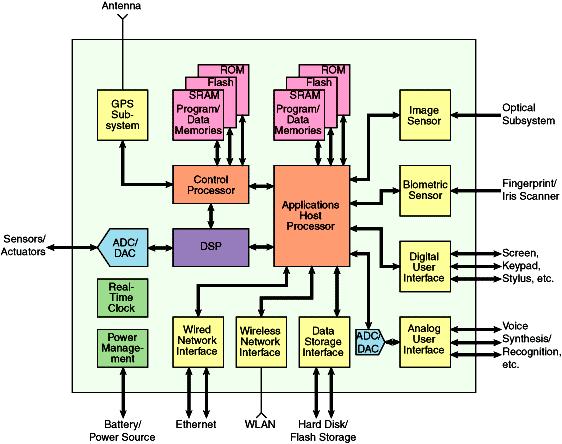
36 A Modern VLSI Device System-on-a-chip (SOC) Data terminal DSP cor e Interface logic RAM ROM Mixedsignal Codec Transmission medium Figure 18.5 (page 605) VLSI Test: Lecture 1 ۳٦
37
38 چالشهاي آزمون SOC ها گستردگي و تنوع در طراحي و تحقق فرآیند آزمون كنترل پذیري رویت پذیري و دسترسي آزمون حجم اطلاعات آزمون ظرفیت كانال آزمونگر مدت زمان آزمون بلوك ھاي بنیادي نامتجانس انجام آزمون در سرعت كاري اتلاف توان در فرآیند آزمون
VLSI Testing. Introduction. Virendra Singh Indian Institute of Science Bangalore
 VLSI Testing Introduction Virendra Singh Indian Institute of Science Bangalore virendra@computer.org E0 286: Test & Verification of SoC Design Lecture - 1 Reading Material Text Book: M.L. Bushnell and
Testing Digital Systems I
 Testing Digital Systems I Lecture 1: Introduction Instructor: M. Tahoori Copyright 2011, M. Tahoori TDS I: Lecture 1 1 Today s Lecture Logistics Course Outline Introduction Copyright 2011, M. Tahoori TDS
VLSI System Testing. Lecture 1 Introduction Class website: people.ee.duke.edu/~krish/teaching/538.html
 ECE 538 VLSI System Testing Krish Chakrabarty Lecture 1: Overview Krish Chakrabarty 1 Lecture 1 Introduction Class website: people.ee.duke.edu/~krish/teaching/538.html VLSI realization process Verification
ENG04057 Teste de Sistema Integrados. Prof. Eric Ericson Fabris (Marcelo Lubaszewski)
") ENG04057 Teste de Sistema Integrados Prof. Eric Ericson Fabris (Marcelo Lubaszewski) Março 2011 Slides adapted from ABRAMOVICI, M.; BREUER, M.; FRIEDMAN, A. Digital Systems Testing and Testable Design.
ENG04057 Teste de Sistema Integrados Prof. Eric Ericson Fabris (Marcelo Lubaszewski) Março 2011 Slides adapted from ABRAMOVICI, M.; BREUER, M.; FRIEDMAN, A. Digital Systems Testing and Testable Design.
EE434 ASIC & Digital Systems Testing
 EE434 ASIC & Digital Systems Testing Spring 2015 Dae Hyun Kim daehyun@eecs.wsu.edu 1 Introduction VLSI realization process Verification and test Ideal and real tests Costs of testing Roles of testing A
Metodologie di progetto HW Il test di circuiti digitali
 Metodologie di progetto HW Il test di circuiti digitali Introduzione Versione del 9/4/8 Metodologie di progetto HW Il test di circuiti digitali Introduction VLSI Realization Process Customer s need Determine
Metodologie di progetto HW Il test di circuiti digitali
 Metodologie di progetto HW Il test di circuiti digitali Introduzione Versione del 9/4/8 Metodologie di progetto HW Il test di circuiti digitali Introduction Pag. 2 VLSI Realization Process Customer s need
About the Instructor
 About the Instructor Kwang-Ting (Tim) Cheng PhD, 1988, Univ. of California, Berkeley 1988-1993: AT&T Bell Labs 1993-Present: Professor, Dept. of ECE, Univ. of California, Santa Barbara 1999-2002: Director,
l Some materials from various sources! Soma 1! l Apply a signal, measure output, compare l 32-bit adder test example:!
 Acknowledgements! Introduction and Overview! Mani Soma! l Some materials from various sources! n Dr. Phil Nigh, IBM! n Principles of Testing Electronic Systems by S. Mourad and Y. Zorian! n Essentials
TESTING AND TESTABLE DESIGN OF DIGITAL SYSTES
 TESTING AND TESTABLE DESIGN OF DIGITAL SYSTES Kewal K. Saluja University of Wisconsin - Madison Motivation, Fault Models and some Callenges Overview Motivation Technology, Test cost, and VLSI realization
COEN-4730 Computer Architecture Lecture 12. Testing and Design for Testability (focus: processors)
") 1 COEN-4730 Computer Architecture Lecture 12 Testing and Design for Testability (focus: processors) Cristinel Ababei Dept. of Electrical and Computer Engineering Marquette University 1 Outline Testing
1 COEN-4730 Computer Architecture Lecture 12 Testing and Design for Testability (focus: processors) Cristinel Ababei Dept. of Electrical and Computer Engineering Marquette University 1 Outline Testing
Hardware Design Environments. Dr. Mahdi Abbasi Computer Engineering Department Bu-Ali Sina University
 Hardware Design Environments Dr. Mahdi Abbasi Computer Engineering Department Bu-Ali Sina University Outline Welcome to COE 405 Digital System Design Design Domains and Levels of Abstractions Synthesis
A Built-in Self-Test for System-on-Chip
 A Built-in Self-Test for System-on-Chip Rashid Rashidzadeh University of Windsor Digital 1 Objective : Design an intellectual property (IP) core which enables low speed Automatic Test Equipment (ATE) to
Chapter 9. Design for Testability
 Chapter 9 Design for Testability Testability CUT = Circuit Under Test A design property that allows: cost-effective development of tests to be applied to the CUT determining the status of the CUT (normal
Digital Integrated Circuits
 Digital Integrated Circuits Lecture Jaeyong Chung System-on-Chips (SoC) Laboratory Incheon National University Design/manufacture Process Chung EPC655 2 Design/manufacture Process Chung EPC655 3 Layout
Lecture 2 VLSI Testing Process and Equipment
 Lecture 2 VLSI Testing Process and Equipment Motivation Types of Testing Test Specifications and Plan Test Programming Test Data Analysis Automatic Test Equipment Parametric Testing Summary VLSI Test:
VLSI Test Technology and Reliability (ET4076)
") VLSI Test Technology and Reliability (ET4076) Lecture 4(part 2) Testability Measurements (Chapter 6) Said Hamdioui Computer Engineering Lab Delft University of Technology 2009-2010 1 Previous lecture What
VLSI Test Technology and Reliability (ET4076) Lecture 4(part 2) Testability Measurements (Chapter 6) Said Hamdioui Computer Engineering Lab Delft University of Technology 2009-2010 1 Previous lecture What
IC Testing and Development in Semiconductor Area
 IC Testing and Development in Semiconductor Area Prepare by Lee Zhang, 2004 Outline 1. Electronic Industry Development 2. Semiconductor Industry Development 4Electronic Industry Development Electronic
VLSI Testing. Virendra Singh. Bangalore E0 286: Test & Verification of SoC Design Lecture - 7. Jan 27,
 VLSI Testing Fault Simulation Virendra Singh Indian Institute t of Science Bangalore virendra@computer.org E 286: Test & Verification of SoC Design Lecture - 7 Jan 27, 2 E-286@SERC Fault Simulation Jan
A Research Paper on Designing a TAP(Test Access Port)
") A Research Paper on Designing a TAP(Test Access Port) 1 Mr. VISHWAS K. CHAUDHARY, 2 Mr. MANISH J. PATEL 1, 2 P. G. Students in M.E.(VLSI & ESD) Gujarat Technological University & Seer-Akademi Ahmedabad,
A Research Paper on Designing a TAP(Test Access Port) 1 Mr. VISHWAS K. CHAUDHARY, 2 Mr. MANISH J. PATEL 1, 2 P. G. Students in M.E.(VLSI & ESD) Gujarat Technological University & Seer-Akademi Ahmedabad,
JTAG TAP CONTROLLER PROGRAMMING USING FPGA BOARD
 JTAG TAP CONTROLLER PROGRAMMING USING FPGA BOARD 1 MOHAMED JEBRAN.P, 2 SHIREEN FATHIMA, 3 JYOTHI M 1,2 Assistant Professor, Department of ECE, HKBKCE, Bangalore-45. 3 Software Engineer, Imspired solutions,
VLSI Test Technology and Reliability (ET4076)
") VLSI Test Technology and Reliability (ET4076) Lecture 8 (1) Delay Test (Chapter 12) Said Hamdioui Computer Engineering Lab Delft University of Technology 2009-2010 1 Learning aims Define a path delay fault
VLSI Test Technology and Reliability (ET4076) Lecture 8 (1) Delay Test (Chapter 12) Said Hamdioui Computer Engineering Lab Delft University of Technology 2009-2010 1 Learning aims Define a path delay fault
Very Large Scale Integration (VLSI)
") Very Large Scale Integration (VLSI) Lecture 10 Dr. Ahmed H. Madian Ah_madian@hotmail.com Dr. Ahmed H. Madian-VLSI 1 Content Manufacturing Defects Wafer defects Chip defects Board defects system defects
Very Large Scale Integration (VLSI) Lecture 10 Dr. Ahmed H. Madian Ah_madian@hotmail.com Dr. Ahmed H. Madian-VLSI 1 Content Manufacturing Defects Wafer defects Chip defects Board defects system defects
VLSI Testing. Fault Simulation. Virendra Singh. Indian Institute of Science Bangalore
 VLSI Testing Fault Simulation Virendra Singh Indian Institute of Science Bangalore virendra@computer.org E0 286: Test & Verification of SoC Design Lecture - 4 Jan 25, 2008 E0-286@SERC 1 Fault Model - Summary
CHAPTER 1 INTRODUCTION
 CHAPTER 1 INTRODUCTION Rapid advances in integrated circuit technology have made it possible to fabricate digital circuits with large number of devices on a single chip. The advantages of integrated circuits
VLSI System Testing. Fault Simulation
 ECE 538 VLSI System Testing Krish Chakrabarty Fault Simulation ECE 538 Krish Chakrabarty Fault Simulation Problem and motivation Fault simulation algorithms Serial Parallel Deductive Concurrent Random
Bibliography. Measuring Software Reuse, Jeffrey S. Poulin, Addison-Wesley, Practical Software Reuse, Donald J. Reifer, Wiley, 1997.
 Bibliography Books on software reuse: 1. 2. Measuring Software Reuse, Jeffrey S. Poulin, Addison-Wesley, 1997. Practical Software Reuse, Donald J. Reifer, Wiley, 1997. Formal specification and verification:
Digital VLSI Testing Prof. Santanu Chattopadhyay Department of Electronics and EC Engineering India Institute of Technology, Kharagpur.
 Digital VLSI Testing Prof. Santanu Chattopadhyay Department of Electronics and EC Engineering India Institute of Technology, Kharagpur Lecture 05 DFT Next we will look into the topic design for testability,
The Boundary - Scan Handbook
 The Boundary - Scan Handbook By Kenneth P. Parker Agilent Technologies * KLUWER ACADEMIC PUBLISHERS Boston / Dordrecht / London TABLE OF CONTENTS List of Figures xiii List of Tables xvi List of Design-for-Test
Testing Principle Verification Testing
 ECE 553: TESTING AND TESTABLE DESIGN OF DIGITAL SYSTES Test Process and Test Equipment Overview Objective Types of testing Verification testing Characterization testing Manufacturing testing Acceptance
Testable SOC Design. Sungho Kang
 Testable SOC Design Sungho Kang 2001.10.5 Outline Introduction SOC Test Challenges IEEE P1500 SOC Test Strategies Conclusion 2 SOC Design Evolution Emergence of very large transistor counts on a single
Mentor Graphics Tools for DFT. DFTAdvisor, FastScan and FlexTest
 Mentor Graphics Tools for DFT DFTAdvisor, FastScan and FlexTest 1 DFT Advisor Synthesis tool capable of doing DRC, Scan Insertion and Test point Synthesis Creates a do file and a test procedure file after
VLSI Testing. Lecture Fall 2003
 VLSI Testing Lecture 25 8-322 Fall 23 Announcement Homework 9 is due next Thursday (/2) Exam II is on Tuesday (/8) in class Review Session: When: Next Monday (/7) afternoon, 4pm 6pm Where: B3, HH 2 Outline
CMOS Testing: Part 1. Outline
 CMOS Testing: Part 1 Introduction Fault models Stuck-line (single and multiple) Bridging Stuck-open Test pattern generation Combinational circuit test generation Sequential circuit test generation ECE
COE 561 Digital System Design & Synthesis Introduction
 1 COE 561 Digital System Design & Synthesis Introduction Dr. Aiman H. El-Maleh Computer Engineering Department King Fahd University of Petroleum & Minerals Outline Course Topics Microelectronics Design
EE 709:Testing & Verification of VLSI Circuits Introduction
 EE 709:Testing & Verification of VLSI Circuits Introduction Virendra Singh Associate Professor Computer Architecture and Dependable Systems Lab Dept. of Electrical Engineering Indian Institute of Technology
Embedded Quality for Test. Yervant Zorian LogicVision, Inc.
 Embedded Quality for Test Yervant Zorian LogicVision, Inc. Electronics Industry Achieved Successful Penetration in Diverse Domains Electronics Industry (cont( cont) Met User Quality Requirements satisfying
INTERCONNECT TESTING WITH BOUNDARY SCAN
 INTERCONNECT TESTING WITH BOUNDARY SCAN Paul Wagner Honeywell, Inc. Solid State Electronics Division 12001 State Highway 55 Plymouth, Minnesota 55441 Abstract Boundary scan is a structured design technique
Graphics: Alexandra Nolte, Gesine Marwedel, Universität Dortmund. RTL Synthesis
 Graphics: Alexandra Nolte, Gesine Marwedel, 2003 Universität Dortmund RTL Synthesis Purpose of HDLs Purpose of Hardware Description Languages: Capture design in Register Transfer Language form i.e. All
Keysight Technologies Expanding IEEE Std Boundary-Scan Architecture Beyond Manufacturing Test of PCBA
 Keysight Technologies Expanding IEEE Std 1149.1 Boundary-Scan Architecture Beyond Manufacturing Test of PCBA Article Reprint This paper was first published in the 2017 IPC APEX Technical Conference, CA,
Design and Synthesis for Test
 TDTS 80 Lecture 6 Design and Synthesis for Test Zebo Peng Embedded Systems Laboratory IDA, Linköping University Testing and its Current Practice To meet user s quality requirements. Testing aims at the
Expanding IEEE Std Boundary-Scan Architecture Beyond Manufacturing Test of Printed Circuit Board Assembly
 Expanding IEEE Std 1149.1 Boundary-Scan Architecture Beyond Manufacturing Test of Printed Circuit Board Assembly Jun Balangue Keysight Technologies Singapore Jun_balangue@keysight.com Abstract This paper
Lecture 28 IEEE JTAG Boundary Scan Standard
 Lecture 28 IEEE 49. JTAG Boundary Scan Standard Motivation Bed-of-nails tester System view of boundary scan hardware Elementary scan cell Test Access Port (TAP) controller Boundary scan instructions Summary
Advanced Digital Logic Design EECS 303
 Advanced igital Logic esign EECS 33 http://ziyang.eecs.northwestern.edu/eecs33/ Teacher: Robert ick Office: L477 Tech Email: dickrp@northwestern.edu Phone: 847 467 2298 Outline. 2. 2 Robert ick Advanced
DFT Trends in the More than Moore Era. Stephen Pateras Mentor Graphics
 DFT Trends in the More than Moore Era Stephen Pateras Mentor Graphics steve_pateras@mentor.com Silicon Valley Test Conference 2011 1 Outline Semiconductor Technology Trends DFT in relation to: Increasing
Built-In Self-Test for Programmable I/O Buffers in FPGAs and SoCs
 Built-In Self-Test for Programmable I/O Buffers in FPGAs and SoCs Sudheer Vemula, Student Member, IEEE, and Charles Stroud, Fellow, IEEE Abstract The first Built-In Self-Test (BIST) approach for the programmable
Chapter 5: ASICs Vs. PLDs
 Chapter 5: ASICs Vs. PLDs 5.1 Introduction A general definition of the term Application Specific Integrated Circuit (ASIC) is virtually every type of chip that is designed to perform a dedicated task.
Lecture 7 Fault Simulation
 Lecture 7 Fault Simulation Problem and motivation Fault simulation algorithms Serial Parallel Deductive Concurrent Random Fault Sampling Summary Copyright 2, Agrawal & Bushnell VLSI Test: Lecture 7 Problem
Contents 1 Basic of Test and Role of HDLs 2 Verilog HDL for Design and Test
 1 Basic of Test and Role of HDLs... 1.1 Design and Test... 1.1.1 RTL Design Process... 1.1.2 Postmanufacturing Test... 1.2 Test Concerns... 1.2.1 Test Methods... 1.2.2 Testability Methods... 1.2.3 Testing
System Verification of Hardware Optimization Based on Edge Detection
 Circuits and Systems, 2013, 4, 293-298 http://dx.doi.org/10.4236/cs.2013.43040 Published Online July 2013 (http://www.scirp.org/journal/cs) System Verification of Hardware Optimization Based on Edge Detection
Evolution of CAD Tools & Verilog HDL Definition
 Evolution of CAD Tools & Verilog HDL Definition K.Sivasankaran Assistant Professor (Senior) VLSI Division School of Electronics Engineering VIT University Outline Evolution of CAD Different CAD Tools for
VLSI Test Technology and Reliability (ET4076)
") VLSI Test Technology and Reliability (ET4076) Lecture 8(2) I DDQ Current Testing (Chapter 13) Said Hamdioui Computer Engineering Lab Delft University of Technology 2009-2010 1 Learning aims Describe the
VLSI Test Technology and Reliability (ET4076) Lecture 8(2) I DDQ Current Testing (Chapter 13) Said Hamdioui Computer Engineering Lab Delft University of Technology 2009-2010 1 Learning aims Describe the
High Quality, Low Cost Test
 Datasheet High Quality, Low Cost Test Overview is a comprehensive synthesis-based test solution for compression and advanced design-for-test that addresses the cost challenges of testing complex designs.
FPGA Based Digital Design Using Verilog HDL
 FPGA Based Digital Design Using Course Designed by: IRFAN FAISAL MIR ( Verilog / FPGA Designer ) irfanfaisalmir@yahoo.com * Organized by Electronics Division Integrated Circuits Uses for digital IC technology
Programmable Logic Devices II
 São José February 2015 Prof. Hoeller, Prof. Moecke (http://www.sj.ifsc.edu.br) 1 / 28 Lecture 01: Complexity Management and the Design of Complex Digital Systems Prof. Arliones Hoeller arliones.hoeller@ifsc.edu.br
DIGITAL DESIGN TECHNOLOGY & TECHNIQUES
 DIGITAL DESIGN TECHNOLOGY & TECHNIQUES CAD for ASIC Design 1 INTEGRATED CIRCUITS (IC) An integrated circuit (IC) consists complex electronic circuitries and their interconnections. William Shockley et
Lecture 3 - Fault Simulation
 Lecture 3 - Fault Simulation Fault simulation Algorithms Serial Parallel Deductive Random Fault Sampling Problem and Motivation Fault simulation Problem: Given A circuit A sequence of test vectors A fault
SoC Design Flow & Tools: SoC Testing
 SoC Design Flow & Tools: SoC Testing Jiun-Lang Huang Graduate Institute of Electronics Engineering Department of Electrical Engineering National Taiwan University Outline l SoC Test Challenges l Test Access
Testability Optimizations for A Time Multiplexed CPLD Implemented on Structured ASIC Technology
 ROMANIAN JOURNAL OF INFORMATION SCIENCE AND TECHNOLOGY Volume 14, Number 4, 2011, 392 398 Testability Optimizations for A Time Multiplexed CPLD Implemented on Structured ASIC Technology Traian TULBURE
Development of a Boundary Scan Test controller creation tool
 Eindhoven University of Technology MASTER'S THESIS Development of a Boundary Scan Test controller creation tool by J.H. Coenen Supervisors: Prof. Ir. M.T.M. Segers Ir. M.N.M. Muris The faculty of Electronical
Impact of DFT Techniques on Wafer Probe
 Impact of DFT Techniques on Wafer Probe Ron Leckie, CEO, INFRASTRUCTURE ron@infras.com Co-author: Charlie McDonald, LogicVision charlie@lvision.com The Embedded Test Company TM Agenda INFRASTRUCTURE Introduction
Department of Electrical and Computer Engineering University of Wisconsin Madison. Fall Midterm Examination CLOSED BOOK
 Department of Electrical and Computer Engineering University of Wisconsin Madison ECE 553: Testing and Testable Design of Digital Systems Fall 2013-2014 Midterm Examination CLOSED BOOK Kewal K. Saluja
Digital Systems Testing
 Digital Systems Testing Verilog HDL for Design and Test Moslem Amiri, Václav Přenosil Embedded Systems Laboratory Faculty of Informatics, Masaryk University Brno, Czech Republic amiri@mail.muni.cz prenosil@fi.muni.cz
Design for Test Methodology Case Study for Motorola C-5e DCP Using the Cadence Incisive Accelerator/Emulator
 Design for Test Methodology Case Study for Motorola C-5e DCP Using the Cadence Incisive Accelerator/Emulator Justin Hernandez SA837/CORP/GSG ZAS37/justin.hernandez@motorola.com Philip Giangarra RU433/SPS/NCSG
Design for Test of Digital Systems TDDC33
 Personnel Design for Test of Digital Systems TDDC33 Erik Larsson - Course leader (examinator) Email: erik.larsson@liu.se Dimitar Nikolov - Course assistant Email: dimitar.nikolov@liu.se Madeleine Häger
Characteristics of the ITC 99 Benchmark Circuits
 Characteristics of the ITC 99 Benchmark Circuits Scott Davidson Sun Microsystems, Inc. ITC 99 Benchmarks - Scott Davidson Page 1 Outline Why Benchmark? Some History. Soliciting Benchmarks Benchmark Characteristics
101-1 Under-Graduate Project Digital IC Design Flow
 101-1 Under-Graduate Project Digital IC Design Flow Speaker: Ming-Chun Hsiao Adviser: Prof. An-Yeu Wu Date: 2012/9/25 ACCESS IC LAB Outline Introduction to Integrated Circuit IC Design Flow Verilog HDL
Faults, Testing & Test Generation
 Faults, Testing & Test Generation Smith Text: Chapter 14.1,14.3, 14.4 Mentor Graphics/Tessent: Scan and ATPG Process Guide ATPG and Failure Diagnosis Tools Reference Manual (access via mgcdocs ) ASIC Design
November 11, 2009 Chang Kim ( 김창식 )
") Test Cost Challenges November 11, 2009 Chang Kim ( 김창식 ) 1 2 Where we are!!! Number of Die per wafer exponentially increasing!! Bigger Wafer Diameter 150mm 200mm 300mm 450mm 2000 2005 2010 2015 1985 1990
Test Cost Challenges November 11, 2009 Chang Kim ( 김창식 ) 1 2 Where we are!!! Number of Die per wafer exponentially increasing!! Bigger Wafer Diameter 150mm 200mm 300mm 450mm 2000 2005 2010 2015 1985 1990
SoC Design Lecture 14: SoC Testing. Shaahin Hessabi Department of Computer Engineering Sharif University of Technology
 SoC Design Lecture 14: SoC Testing Shaahin Hessabi Department of Computer Engineering Sharif University of Technology Outline Introduction to Testing Importance of SoC Testing Challenges of SoC Testing
Outline of Presentation
 Built-In Self-Test for Programmable I/O Buffers in FPGAs and SoCs Sudheer Vemula and Charles Stroud Electrical and Computer Engineering Auburn University presented at 2006 IEEE Southeastern Symp. On System
Accessing On-chip Instruments Through the Life-time of Systems ERIK LARSSON
 Accessing On-chip Instruments Through the Life-time of Systems ERIK LARSSON Motivation We know: Electronics is used everywhere Transistors increase in number and decrease in size It leads to: Many possible
DSP-design ERIK LARSSON
 DSP-design ERIK LRSSON Product we use and depend on .include electronics Integrated circuit Printed-circuit-board System nalog Input Muxing C S S B 2 rray of nalog PSoC Blocks SRM Memory P C S B S 2 Decimator
CAD for VLSI. Debdeep Mukhopadhyay IIT Madras
 CAD for VLSI Debdeep Mukhopadhyay IIT Madras Tentative Syllabus Overall perspective of VLSI Design MOS switch and CMOS, MOS based logic design, the CMOS logic styles, Pass Transistors Introduction to Verilog
Page 1. Outline. A Good Reference and a Caveat. Testing. ECE 254 / CPS 225 Fault Tolerant and Testable Computing Systems. Testing and Design for Test
 Page Outline ECE 254 / CPS 225 Fault Tolerant and Testable Computing Systems Testing and Design for Test Copyright 24 Daniel J. Sorin Duke University Introduction and Terminology Test Generation for Single
EITF35: Introduction to Structured VLSI Design
 EITF35: Introduction to Structured VLSI Design Part 1.1.2: Introduction (Digital VLSI Systems) Liang Liu liang.liu@eit.lth.se 1 Outline Why Digital? History & Roadmap Device Technology & Platforms System
UNIT IV CMOS TESTING
 UNIT IV CMOS TESTING 1. Mention the levels at which testing of a chip can be done? At the wafer level At the packaged-chip level At the board level At the system level In the field 2. What is meant by
Design Verification Lecture 01
 M. Hsiao 1 Design Verification Lecture 01 Course Title: Verification of Digital Systems Professor: Michael Hsiao (355 Durham) Prerequisites: Digital Logic Design, C/C++ Programming, Data Structures, Computer
Synchronization In Digital Systems
 2011 International Conference on Information and Network Technology IPCSIT vol.4 (2011) (2011) IACSIT Press, Singapore Synchronization In Digital Systems Ranjani.M. Narasimhamurthy Lecturer, Dr. Ambedkar
Glossary. ATPG -Automatic Test Pattern Generation. BIST- Built-In Self Test CBA- Cell Based Array
 Glossary ATPG -Automatic Test Pattern Generation BFM - Bus Functional Model BIST- Built-In Self Test CBA- Cell Based Array FSM - Finite State Machine HDL- Hardware Description Language ISA (ISS) - Instruction
Hardware Modeling using Verilog Prof. Indranil Sengupta Department of Computer Science and Engineering Indian Institute of Technology, Kharagpur
 Hardware Modeling using Verilog Prof. Indranil Sengupta Department of Computer Science and Engineering Indian Institute of Technology, Kharagpur Lecture 01 Introduction Welcome to the course on Hardware
IEEE P1500, a Standard for System on Chip DFT
 page 1(6) IEEE P1500, a Standard for System on Chip DFT Kim Petersén HDC, Hardware Design Center 723 50 Västerås Sweden Email: kim.petersen@hdc.se key words: IP, DFT, SoC, BIST, BISR ABSTRACT This document
Y. Tsiatouhas. VLSI Systems and Computer Architecture Lab
 CMOS INTEGRATED CIRCUIT DESIGN TECHNIQUES University of Ioannina VLSI Testing Dept. of Computer Science and Engineering Y. Tsiatouhas CMOS Integrated Circuit Design Techniques Overview 1. VLSI testing
ASIC world. Start Specification Design Verification Layout Validation Finish
 AMS Verification Agenda ASIC world ASIC Industrial Facts Why Verification? Verification Overview Functional Verification Formal Verification Analog Verification Mixed-Signal Verification DFT Verification
01 1 Electronic Design Automation (EDA) the correctness, testability, and compliance of a design is checked by software
 the correctness, testability, and compliance of a design is checked by software") 01 1 Electronic Design Automation (EDA) 01 1 Electronic Design Automation (EDA): (Short Definition) The use of software to automate electronic (digital and analog) design. Electronic Design Automation
01 1 Electronic Design Automation (EDA) 01 1 Electronic Design Automation (EDA): (Short Definition) The use of software to automate electronic (digital and analog) design. Electronic Design Automation
EECS150 - Digital Design Lecture 5 - Verilog Logic Synthesis
 EECS150 - Digital Design Lecture 5 - Verilog Logic Synthesis Jan 31, 2012 John Wawrzynek Spring 2012 EECS150 - Lec05-verilog_synth Page 1 Outline Quick review of essentials of state elements Finite State
Y. Tsiatouhas. VLSI Systems and Computer Architecture Lab. Embedded Core Testing (ΙΕΕΕ SECT std) 2
 2") CMOS INTEGRATED CIRCUIT DESIGN TECHNIQUES University of Ioannina Embedded Testing (ΙΕΕΕ 1500 Std. SECT) Dept. of Computer Science and Engineering Y. Tsiatouhas CMOS Integrated Circuit Design Techniques
CMOS INTEGRATED CIRCUIT DESIGN TECHNIQUES University of Ioannina Embedded Testing (ΙΕΕΕ 1500 Std. SECT) Dept. of Computer Science and Engineering Y. Tsiatouhas CMOS Integrated Circuit Design Techniques
Evaluation of FPGA Resources for Built-In Self-Test of Programmable Logic Blocks
 Evaluation of FPGA Resources for Built-In Self-Test of Programmable Logic Blocks Charles Stroud, Ping Chen, Srinivasa Konala, Dept. of Electrical Engineering University of Kentucky and Miron Abramovici
SCANWORKS TEST DEVELOPMENT STATION BUNDLE
 SCANWORKS TEST DEVELOPMENT STATION BUNDLE The ScanWorks Test Development Station is the most powerful set of boundary-scan test development and application tools available. It not only includes all the
outline Reliable State Machines MER Mission example
 outline Reliable State Machines Dr. Gary R Burke California Institute of Technology Jet Propulsion Laboratory Background JPL MER example JPL FPGA/ASIC Process Procedure Guidelines State machines Traditional
Test and Measurement Challenges for 3D IC Development. R. Robertazzi IBM Research
 Test and Measurement Challenges for 3D IC Development R. Robertazzi IBM Research PFA Bill Price. Pete Sorce. John Ott. David Abraham. Pavan Samudrala Digital Test Kevin Stawaisz. TEL P12 Prober Glen Lansman,
Bulletproofing FSM Verification Automated Approach to Detect Corner Case Issues in an FSM Design
 Bulletproofing FSM Verification Automated Approach to Detect Corner Case Issues in an FSM Design Lisa Piper Technical Marketing Real Intent Inc., Sunnyvale, CA Comprehensive verification of Finite State
BIST-Based Test and Diagnosis of FPGA Logic Blocks
 IEEE TRANSACTIONS ON VERY LARGE SCALE INTEGRATION (VLSI) SYSTEMS, VOL. 9, NO. 1, FEBRUARY 2001 159 BIST-Based Test and Diagnosis of FPGA Logic Blocks Miron Abramovici, Fellow, IEEE, and Charles E. Stroud,
Choosing an Intellectual Property Core
 Choosing an Intellectual Property Core MIPS Technologies, Inc. June 2002 One of the most important product development decisions facing SOC designers today is choosing an intellectual property (IP) core.
Advanced FPGA Design Methodologies with Xilinx Vivado
 Advanced FPGA Design Methodologies with Xilinx Vivado Alexander Jäger Computer Architecture Group Heidelberg University, Germany Abstract With shrinking feature sizes in the ASIC manufacturing technology,
International Journal of Digital Application & Contemporary research Website: (Volume 1, Issue 7, February 2013)
") Programmable FSM based MBIST Architecture Sonal Sharma sonal.sharma30@gmail.com Vishal Moyal vishalmoyal@gmail.com Abstract - SOCs comprise of wide range of memory modules so it is not possible to test
Programmable FSM based MBIST Architecture Sonal Sharma sonal.sharma30@gmail.com Vishal Moyal vishalmoyal@gmail.com Abstract - SOCs comprise of wide range of memory modules so it is not possible to test
Columbia Univerity Department of Electrical Engineering Fall, 2004
 Columbia Univerity Department of Electrical Engineering Fall, 2004 Course: EE E4321. VLSI Circuits. Instructor: Ken Shepard E-mail: shepard@ee.columbia.edu Office: 1019 CEPSR Office hours: MW 4:00-5:00
Digital Design Methodology (Revisited) Design Methodology: Big Picture
 Design Methodology: Big Picture") Digital Design Methodology (Revisited) Design Methodology Design Specification Verification Synthesis Technology Options Full Custom VLSI Standard Cell ASIC FPGA CS 150 Fall 2005 - Lec #25 Design Methodology
Digital Design Methodology (Revisited) Design Methodology Design Specification Verification Synthesis Technology Options Full Custom VLSI Standard Cell ASIC FPGA CS 150 Fall 2005 - Lec #25 Design Methodology
SSoCC'01 4/3/01. Specific BIST Architectures. Gert Jervan Embedded Systems Laboratory (ESLAB) Linköping University
 Linköping University") Specific BIST Architectures Gert Jervan Embedded Systems Laboratory (ESLAB) Linköping University General Concepts Test-per-scan architectures Multiple scan chains Test-per-clock architectures BIST conclusions
Specific BIST Architectures Gert Jervan Embedded Systems Laboratory (ESLAB) Linköping University General Concepts Test-per-scan architectures Multiple scan chains Test-per-clock architectures BIST conclusions
Implementation of FPGA for Decision Making for IC S Library
 Implementation of FPGA for Decision Making for IC S Library Sanjay Chowdhary 1, Shashidhar P.K 2, Manjunathraddi Bentur 3, Sunil Begumpur 4 1, 2, 3, 4 Dept. of Electronic and Communication, SKSVMACET Laxmeshwar,