Graser User Conference Only
|
|
|
- Leslie Knight
- 5 years ago
- Views:
Transcription
 Mika Ho / Graser")
1 High-Speed Interface Driven PCB Design (Net Group, Aixx, Floorplanning etc) Mika Ho / Graser 31/Oct/2014
2 Topic Chapter One An Interface Example DDRx An Example: Timing Relationship for DDR3 Case Description Routing condition Using features Before Interactive Routing You must define well You might need to define well
3 Topic Chapter Two Net Groups CPU[0]_BANK[0] CHNLA_ADDR_CMD CHNLB_ADDR_CMD CHNLA_CLOCKS CHNLB_CLOCKS CHNLA_CTRL CHNLB_CTRL CHNLA_DATA CHNLB_DATA Plan 1 st CLOCKS 2 nd Target Pre-routing 3 rd ADDR CMD & CLTR 4 th DATA Routing Result Conclusion What Else?
4 Topic Chapter Three Routing Flow Optimize Timing vision Auto-interactive Delay Tune (AiDT) Auto-interactive Phase Tune (AiPT) Auto-interactive Add Connect (AiAC) Auto-interactive Convert Corner (AiCC) Auto-interactive Breakout (AiBT) Auto-interactive Trunk Routing (AiTR)
5 Chapter One

6 An Interface Example - DDRx PCB designers need to connect interfaces quickly and easily Today s interfaces cannot be modeled in single-level hierarchy Memory Controller IC byte lane 0 byte lane 1 byte lane 2 byte lane 3 byte lane 4 byte lane 5 byte lane 6 byte lane 7 Memory Devices DATA signals DQ<7..0> byte lane x Strobe signals DQS_P & DQS_N Mask signal DQM

7 Timing closure on advanced highspeed interfaces is iterative, frustrating, and time consuming Market demands products that are faster, have more bandwidth, and use less power Increasing use of standards-based interfaces DDR2 DDR3 DDR4 PCI Express Gen1 Gen2 Gen3 Supply voltage: 1.8V 1.5V 1.2V MEM CTRLR Differential Clock Data Bytelane (5) Differential Clock D I Data Bytelane (5) M M Address / Command / Control Address / Command / Control Differential Clock Data Bytelane (4) V T T VTT VTT D I M M V T T VTT Increasingly sensitive signals Ripples through power supply Crosstalk Complex set of electrical and layout implementation constraints Differential Clock Data Bytelane (4) VTT


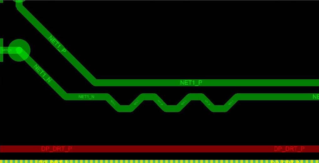
8 An Example: Timing Relationship for DDR3 Data ADDR/CMD CONTROL Strobe CLOCKS CLOCKS CLOCKS Complex matching requirements 4 sets of clocks, 8 sets of strobes Match CLKs, strobes, and data AND Match CLKs, ADDR/CMD, and CONTROL Memory Controller CONTROL ADDR/CMD Clocks DATA ODT DRAM TERMINATION
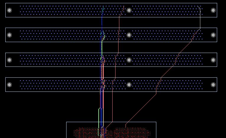
![Case Description Routing Condition : DDR Portion Area: Critical Signal: Net Group: CPU[0]_BANK[0]-CHNLA_ADDR_CMD (24) CPU[0]_BANK[0]-CHNLB_ADDR_CMD (24) CPU[0]_BANK[0]-CHNLA_CLOCKS (8)](/docs-images/87/95587437/images/9-2.jpg "CPU[0]_BANK[0]-CHNLB_CLOCKS (8) CPU[0]_BANK[0]-CHNLA_CTRL (16) CPU[0]_BANK[0]-CHNLB_CTRL (16) CPU[0]_BANK[0]-CHNLA_DATA (90) CPU[0]_BANK[0]-CHNLB_DATA (90) Total: 276 nets Stackup: 12")
9 Case Description Routing Condition : DDR Portion Area: Critical Signal: Net Group: CPU[0]_BANK[0]-CHNLA_ADDR_CMD (24) CPU[0]_BANK[0]-CHNLB_ADDR_CMD (24) CPU[0]_BANK[0]-CHNLA_CLOCKS (8) CPU[0]_BANK[0]-CHNLB_CLOCKS (8) CPU[0]_BANK[0]-CHNLA_CTRL (16) CPU[0]_BANK[0]-CHNLB_CTRL (16) CPU[0]_BANK[0]-CHNLA_DATA (90) CPU[0]_BANK[0]-CHNLB_DATA (90) Total: 276 nets Stackup: 12 layers

10 Case Description Using features Allegro PCB Designer v16.6 s034 Design Planning Option High-Speed Option
11 Before Interactive Routing You must define well Constraints Regions Keep in/out areas Fanout Routing layer You might need to define well Cooper in power plane layers
12 Chapter Two
")
13 Net Groups (Enhanced by QIR#5) CPU[0]_BANK[0]

14 Net Groups CPU[0]_BANK[0]

15 Net Groups CPU[0]_BANK[0] Hierarchy : Top Level
16 Net Groups CPU[0]_BANK[0] Down Hierarchy
17 Net Groups CPU[0]_BANK[0] Down Hierarchy : Mid Level
18 Net Groups CPU[0]_BANK[0] Hierarchy : Bottom Level
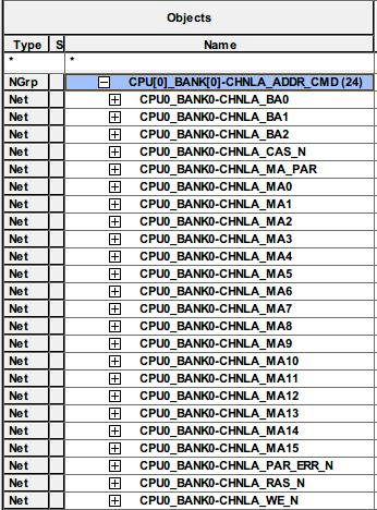
19 Net Groups CPU[0]_BANK[0]-CHNLA_ADDR_CMD
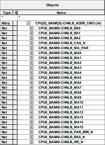
20 Net Groups CPU[0]_BANK[0]-CHNLB_ADDR_CMD
21 Net Groups CPU[0]_BANK[0]-CHNLA_CLOCKS


22 Net Groups CPU[0]_BANK[0]-CHNLB_CLOCKS

23 Net Groups CPU[0]_BANK[0]-CHNLA_CTRL

24 Net Groups CPU[0]_BANK[0]-CHNLB_CTRL

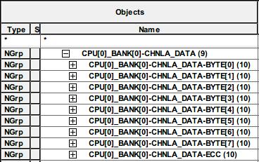
25 Net Groups CPU[0]_BANK[0]-CHNLA_DATA


26 Net Groups CPU[0]_BANK[0]-CHNLB_DATA


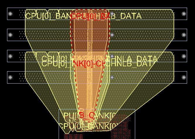
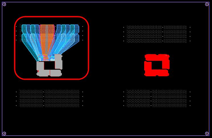
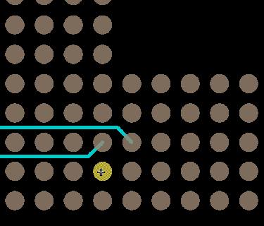
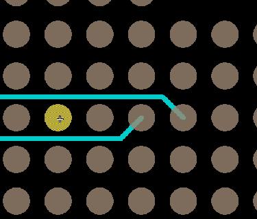
27 Net Groups and Placement Quick and easy way to verify your placement The container gives you a way to visualize the overall routing domain of the interface Visual placement checks let you see parts out-of-place The polygon envelops ALL the pins of nets in the net group TERMINATOR IS OUT OF PLACE TERMINATION BELONGS HERE

 1")

28 Plan (Design Planning Option) 1 st CLOCKS (Channel A & B)


29 Plan (Design Planning Option) 1 st CLOCKS (Channel A & B) - Timing vision (High-Speed option)

 1")


30 Plan (Design Planning Option) 1 st CLOCKS (Channel A & B) - AiPT (High-Speed option)

 2")
31 Plan (Design Planning Option) 2 nd Target pre-routing
")

32 Plan (Design Planning Option) 3 rd ADDR CMD & CTRL (Channel A & B)
 - Timing vision (High-Speed")
33 Plan (Design Planning Option) 3 rd ADDR CMD & CTRL (Channel A & B) - Timing vision (High-Speed option)
 - AiDT(High-Speed")
34 Plan (Design Planning Option) 3 rd ADDR CMD & CTRL (Channel A & B) - AiDT(High-Speed option)
 3 rd ADDR CMD")

35 Plan (Design Planning Option) 3 rd ADDR CMD & CTRL (Channel A & B) - AiDT(High-Speed option)


36 Plan (Design Planning Option) 4 th DATA (Channel A & B)
 -")
37 Plan (Design Planning Option) 4 th DATA (Channel A & B) - Unplanning
 - Manual add connection")
38 Plan (Design Planning Option) 4 th DATA (Channel A & B) - Manual add connection
 - Timing vision (High-Speed option) - DRC Phase")
39 Plan (Design Planning Option) 4 th DATA (Channel A & B) - Timing vision (High-Speed option) - DRC Phase view
 - AiPT(High-Speed")
40 Plan (Design Planning Option) 4 th DATA (Channel A & B) - AiPT(High-Speed option)
 - AiPT(High-Speed")
41 Plan (Design Planning Option) 4 th DATA (Channel A & B) - AiPT(High-Speed option)
 - Manual Phase")
42 Plan (Design Planning Option) 4 th DATA (Channel A & B) - Manual Phase Tuning
 - Timing vision (High-Speed option) - DRC Timing")
43 Plan (Design Planning Option) 4 th DATA (Channel A & B) - Timing vision (High-Speed option) - DRC Timing view
 - AiDT (High-Speed option) -")
44 Plan (Design Planning Option) 4 th DATA (Channel A & B) - AiDT (High-Speed option) - Sig1 layer
 - AiDT (High-Speed option) -")
45 Plan (Design Planning Option) 4 th DATA (Channel A & B) - AiDT (High-Speed option) - Sig1 layer
46 Plan (Design Planning Option) 4 th DATA (Channel A & B) - AiDT (High-Speed option) - Sig2 layer
 - AiDT (High-Speed option) -")
47 Plan (Design Planning Option) 4 th DATA (Channel A & B) - AiDT (High-Speed option) - Sig2 layer
 - AiDT (High-Speed option) -")
48 Plan (Design Planning Option) 4 th DATA (Channel A & B) - AiDT (High-Speed option) - Sig3 layer
 4 th DATA")
 -")
49 Plan (Design Planning Option) 4 th DATA (Channel A & B) - AiDT (High-Speed option) - Sig3 layer
50 Plan (Design Planning Option) 4 th DATA (Channel A & B) - AiDT (High-Speed option) - Sig4 layer
 - AiDT (High-Speed option) -")
51 Plan (Design Planning Option) 4 th DATA (Channel A & B) - AiDT (High-Speed option) - Sig4 layer
52 Plan (Design Planning Option) 4 th DATA (Channel A & B) - AiDT (High-Speed option) - Sig5 layer
 - AiDT (High-Speed option) -")
53 Plan (Design Planning Option) 4 th DATA (Channel A & B) - AiDT (High-Speed option) - Sig5 layer
 4 th DATA")

54 Plan (Design Planning Option) 4 th DATA (Channel A & B) - Manual fine tuning + AiDT - Sig5 layer
 - Manual fine tuning + AiDT -")
55 Plan (Design Planning Option) 4 th DATA (Channel A & B) - Manual fine tuning + AiDT - Sig5 layer
 - AiDT (High-Speed option) -")
56 Plan (Design Planning Option) 4 th DATA (Channel A & B) - AiDT (High-Speed option) - Sig6 layer
 - AiDT (High-Speed option) -")
57 Plan (Design Planning Option) 4 th DATA (Channel A & B) - AiDT (High-Speed option) - Sig6 layer

58 Routing Result Timing view

59 Routing Result Phase view
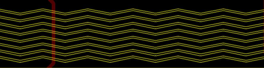
60 Conclusion DDR (276 Nets) Setting Time: About 30 ~ 120 mins Automation Time : About 40 ~ 60 mins Manual Time: About 2 ~ 6 hrs This case : Took 5 hrs

61 What else
62 Chapter Three


63 Routing Flow Fan out Break out Route Plan Route Optimize
 (Enhanced by")
64 Optimize Auto-interactive Delay Tune (AiDT High Speed Option) (Enhanced by QIR#4)


65 Optimize Auto-interactive Phase Tune (AiPT High Speed Option) (Enhanced by QIR#4)


66 Optimize Auto-interactive Add Connect (AiAC PCB Designer) Scribble Mode (Enhanced by QIR#7) Off angle fit Exact fit
 Scribble Mode (Enhanced by")
67 Optimize Auto-interactive Add Connect (AiAC PCB Designer) Scribble Mode (Enhanced by QIR#7)


68 Optimize Auto-interactive Convert Corner (AiCC PCB Designer)


 analysis Canvas-driven inputs for direction, distance, sequence Rat ordering")
69 Optimize Auto-interactive Breakout (AiBT Design Planning Option) (Enhanced by QIR#6) For enterprise customers who design PCBs with high-speed interfaces such as DDR3, PCI Express 3.0, SATA, HDMI, USB 3, XAUI, SFP+ Helps you plan breakout of both components tied to an interface Reduce routing steps and improve efficiency Interface breakout (both ends) analysis Canvas-driven inputs for direction, distance, sequence Rat ordering and layering Split Views allows working on both ends of an interface zoomed-in
 (Enhanced by QIR#7) New Auto-Interactive function")

 3 Accelerates time to breakout and")
70 Optimize Auto-interactive Trunk Routing (AiTR Design Planning Option) (Enhanced by QIR#7) New Auto-Interactive function designed to route the trunk or main section of an interface 1 2 Works with Auto-interactive Breakout Tuning Flow the Bundle Run Auto-Interactive Breakout on both ends Trunk Route follows bundle path (approximately) 3 Accelerates time to breakout and route an interface
Do not hesitate to contact us in case you have questions or need more information
 Working with highspeed PCB Design in OrCAD This guide walks through some of the highspeed PCB Design functionality that is available within OrCAD PCB Editor. The are more functionality available than what
Cadence FPGA System Planner technologies are available in the following product offerings: Allegro FPGA System Planner L, XL, and GXL
 DATASHEET The Cadence FPGA addresses the challenges that engineers encounter when designing one or more large-pin-count FPGAs on the PCB board which includes creating the initial pin assignment, integrating
High-Speed DDR4 Memory Designs and Power Integrity Analysis
 High-Speed DDR4 Memory Designs and Power Integrity Analysis Cuong Nguyen Field Application Engineer cuong@edadirect.com www.edadirect.com 2014 1 PCB Complexity is Accelerating Use of Advanced Technologies
Electrical optimization and simulation of your PCB design
 Electrical optimization and simulation of your PCB design Steve Gascoigne Senior Consultant at Mentor Graphics Zagreb, 10. lipnja 2015. Copyright CADCAM Group 2015 The Challenge of Validating a Design..
Cadence SPB: What s New in 16.6 QIR 8 (HotFix 38)
") Cadence SPB: What s New in 16.6 QIR 8 (HotFix 38) This document describes the new features and enhancements in Cadence SPB products in 16.6 Quarterly Incremental Release (QIR) 8- HotFix38. The products
Cadence SPB: What s New in 16.6 QIR 8 (HotFix 38) This document describes the new features and enhancements in Cadence SPB products in 16.6 Quarterly Incremental Release (QIR) 8- HotFix38. The products
Cadence SPB: What s New in 16.6 Quarterly Incremental Release 003
 Cadence SPB: What s New in 16.6 Quarterly Incremental Release 003 This document describes the new features and enhancements in Cadence SPB products in 16.6 Quarterly Incremental Release (QIR) 3. The products
DDR4 Design And Verification In Hyperlynx LINESIM/Boardsim
 DDR4 Design And Verification In Hyperlynx LINESIM/Boardsim Rod Strange Business Development Manager Teraspeed Consulting A Division of Samtec April 2016 Outline Objective/Goal DDR4 vs. DDR3 from the SI/PI
Introduction to Zynq
 Introduction to Zynq Lab 2 PS Config Part 1 Hello World October 2012 Version 02 Copyright 2012 Avnet Inc. All rights reserved Table of Contents Table of Contents... 2 Lab 2 Objectives... 3 Experiment 1:
Building Differentiated Products Through Shorter, More Predictable Design Cycles
 Building Differentiated Products Through Shorter, More Predictable Design Cycles To position themselves for growth in today s market, systems companies need to build highly differentiated products; reduce
Chip/Package/Board Interface Pathway Design and Optimization. Tom Whipple Product Engineering Architect November 2015
 Chip/Package/Board Interface Pathway Design and Optimization Tom Whipple Product Engineering Architect November 2015 Chip/package/board interface pathway design and optimization PCB design with Allegro
Hardware Design Guidelines for Freescale s High-Performance Digital Signal Processors
 June 2010 Hardware Design Guidelines for Freescale s High-Performance Digital Signal Processors Colin McEwan Systems and Applications Engineer Agenda Introduction and Review Agenda The Freescale AMC ECO-System
Board Design Guidelines for PCI Express Architecture
 Board Design Guidelines for PCI Express Architecture Cliff Lee Staff Engineer Intel Corporation Member, PCI Express Electrical and Card WGs The facts, techniques and applications presented by the following
Designing High-Speed Memory Subsystem DDR. using. Cuong Nguyen. Field Application Engineer
 Designing High-Speed Memory Subsystem using DDR Cuong Nguyen Field Application Engineer cuong@edadirect.com www.edadirect.com 2014 1 Your Design for Excellence Partner Since 1997 EDA Direct has helped
THREE THINGS TO CONSIDER WHEN DESIGNING ELECTRONIC PRODUCTS WITH HIGH-SPEED CONSTRAINTS BY: PATRICK CARRIER, MENTOR GRAPHICS CORP.
 THREE THINGS TO CONSIDER WHEN DESIGNING ELECTRONIC PRODUCTS WITH HIGH-SPEED CONSTRAINTS BY: PATRICK CARRIER, MENTOR GRAPHICS CORP. P A D S W H I T E P A P E R w w w. p a d s. c o m INTRODUCTION Designing
FlowCAD Schweiz AG. Tel Fax STANDARD PROFESSIONAL ALLEGRO. Licensing httpfloating Networked License
 Licensing Floating Networked License : 12 Months Maintenance Support Included In Purchase Price SCHEMATIC ENTRY + DATA MANAGEMENT Graphical, flat and hierarchical page editor and Picture block hierarchy
Technical Note DDR2 (Point-to-Point) Package Sizes and Layout Basics
 Package Sizes and Layout Basics") Introduction Technical Note DDR2 (Point-to-Point) Package Sizes and Layout Basics Introduction Point-to-point designers face many challenges when laying out a new printed circuit board (PCB). The designer
Introduction Technical Note DDR2 (Point-to-Point) Package Sizes and Layout Basics Introduction Point-to-point designers face many challenges when laying out a new printed circuit board (PCB). The designer
HYPERLYNX DDR3 Wizard
 HYPERLYNX DDR3 Wizard w w w. m e n t o r. c o m HyperLynx DDR3 Wizard Virtual Lab Exercise Guide This tutorial outlines the steps for completing a DDR3 Wizard DDR analysis example in HyperLynx BoardSim.
Allegro Sigrity SI Streamlining the creation of high-speed interconnect on digital PCBs and IC packages
 Streamlining the creation of high-speed interconnect on digital PCBs and IC packages The Cadence Allegro Sigrity signal integrity (SI) integrated high-speed design and analysis environment streamlines
High Performance DDR4 interfaces with FPGA Flexibility. Adrian Cosoroaba and Terry Magee Xilinx, Inc.
 High Performance DDR4 interfaces with FPGA Flexibility Adrian Cosoroaba and Terry Magee Xilinx, Inc AGENDA System Requirements for FPGA based systems Higher Bandwidth, Increased Flexibility, Lower Power
HyperLynx DDRx Interface Analysis. Student Workbook
 HyperLynx DDRx Interface Analysis Student Workbook 2017 Mentor Graphics Corporation All rights reserved. This document contains information that is trade secret and proprietary to Mentor Graphics Corporation
Real Time Embedded Systems
 Real Time Embedded Systems " Memories " rene.beuchat@epfl.ch LAP/ISIM/IC/EPFL Chargé de cours LSN/hepia Prof. HES 1998-2008 2 General classification of electronic memories Non-volatile Memories ROM PROM
Symbol Parameter Min Typ Max VDD_CORE Core power 0.9V 1.0V 1. 1V. VDD33 JTAG/FLASH power 2.97V 3.3V 3.63V
 1 Introduction The user guide provides guidelines on how to help you successfully design the CME-M7 board which includes the power supply, configuration, clock, DDR2 or DDR3, high speed USB, LVDS and ADC
Increase Productivity and Quality by New Layout Flow
 Increase Productivity and Quality by New Layout Flow Jonathan / Graser 16 / Oct / 2015 Design Process Introduction CONSTRAINTS PLACEMENT FANOUT BREAKOUT ROUTING DELAY (ATE) NET-GROUP Topology & Delay Physical
IMM64M72D1SCS8AG (Die Revision D) 512MByte (64M x 72 Bit)
 512MByte (64M x 72 Bit)") Product Specification Rev. 1.0 2015 IMM64M72D1SCS8AG (Die Revision D) 512MByte (64M x 72 Bit) RoHS Compliant Product Product Specification 1.0 1 IMM64M72D1SCS8AG Version: Rev. 1.0, MAY 2015 1.0 - Initial
Product Specification Rev. 1.0 2015 IMM64M72D1SCS8AG (Die Revision D) 512MByte (64M x 72 Bit) RoHS Compliant Product Product Specification 1.0 1 IMM64M72D1SCS8AG Version: Rev. 1.0, MAY 2015 1.0 - Initial
ADQVD1B16. DDR2-800+(CL4) 240-Pin EPP U-DIMM 2GB (256M x 64-bits)
 240-Pin EPP U-DIMM 2GB (256M x 64-bits)") General Description ADQVD1B16 DDR2-800+(CL4) 240-Pin EPP U-DIMM 2GB (256M x 64-bits) The ADATA s ADQVD1B16 is a 256Mx64 bits 2GB(2048MB) DDR2-800(CL4) SDRAM EPP memory module, The SPD is programmed to
General Description ADQVD1B16 DDR2-800+(CL4) 240-Pin EPP U-DIMM 2GB (256M x 64-bits) The ADATA s ADQVD1B16 is a 256Mx64 bits 2GB(2048MB) DDR2-800(CL4) SDRAM EPP memory module, The SPD is programmed to
Agilent Bead Probe Technology
 Agilent Bead Probe Technology Page 1 Abstract Lead-free, shrinking geometries, new packages and high-speed signaling present new challenges for ICT. The impact will be more defects, loss of access, lower
Integrating ADS into a High Speed Package Design Process
 Integrating ADS into a High Speed Package Design Process Page 1 Group/Presentation Title Agilent Restricted Month ##, 200X Agenda High Speed SERDES Package Design Requirements Performance Factor and Design
Intel and Intel I/O Processors
 Intel 81341 and Intel 81342 I/O Processors Design Guide May 2007 Order Number: 315054-002US Legal Lines and Disclaimers INFORMATION IN THIS DOCUMENT IS PROVIDED IN CONNECTION WITH INTEL PRODUCTS. NO LICENSE,
FlowCAD Schweiz AG. Tel. +41 (0) Fax +41 (0) OrCAD Professional. Allegro Designer. OrCAD Standard
 Fax +41 (0) OrCAD Professional. Allegro Designer. OrCAD Standard") Licensing Floating Networked License 12 Months Maintenance Support Included In Purchase Price SCHEMATIC ENTRY + DATA MANAGEMENT Graphical, flat and hierarchical page editor and Picture block hierarchy
Licensing Floating Networked License 12 Months Maintenance Support Included In Purchase Price SCHEMATIC ENTRY + DATA MANAGEMENT Graphical, flat and hierarchical page editor and Picture block hierarchy
APPROVAL SHEET. Apacer Technology Inc. Apacer Technology Inc. CUSTOMER: 研華股份有限公司 APPROVED NO. : T0031 PCB PART NO. :
 Apacer Technology Inc. CUSTOMER: 研華股份有限公司 APPROVAL SHEET APPROVED NO. : 90003-T0031 ISSUE DATE MODULE PART NO. : July-28-2011 : 78.02GC6.AF0 PCB PART NO. : 48.18220.090 IC Brand DESCRIPTION : Hynix : DDR3
IMM64M64D1SOD16AG (Die Revision D) 512MByte (64M x 64 Bit)
 512MByte (64M x 64 Bit)") Product Specification Rev. 2.0 2015 IMM64M64D1SOD16AG (Die Revision D) 512MByte (64M x 64 Bit) 512MB DDR Unbuffered SO-DIMM RoHS Compliant Product Product Specification 2.0 1 IMM64M64D1SOD16AG Version:
Product Specification Rev. 2.0 2015 IMM64M64D1SOD16AG (Die Revision D) 512MByte (64M x 64 Bit) 512MB DDR Unbuffered SO-DIMM RoHS Compliant Product Product Specification 2.0 1 IMM64M64D1SOD16AG Version:
AM43xx EMIF Tools. Application Report. Trademarks. Siva Kothamasu
 Application Report Siva Kothamasu ABSTRACT At the center of every application is the need for memory. With limited on-chip processor memory, external memory serves as a solution for large software systems
Features. DDR3 Registered DIMM Spec Sheet
 Features DDR3 functionality and operations supported as defined in the component data sheet 240-pin, Registered Dual In-line Memory Module (RDIMM) Fast data transfer rates: PC3-8500, PC3-10600, PC3-12800
Placement & Routing. Lab 8. Placing Parts
 Placement & Routing Lab 8 Placing Parts 121 Placement and Routing Lab 8: Placing Parts This lesson will show you how to place parts in PADS Layout. Placement can be driven from the schematic or directly
IMM128M72D1SOD8AG (Die Revision F) 1GByte (128M x 72 Bit)
 1GByte (128M x 72 Bit)") Product Specification Rev. 1.0 2015 IMM128M72D1SOD8AG (Die Revision F) 1GByte (128M x 72 Bit) 1GB DDR Unbuffered SO-DIMM RoHS Compliant Product Product Specification 1.0 1 IMM128M72D1SOD8AG Version: Rev.
Product Specification Rev. 1.0 2015 IMM128M72D1SOD8AG (Die Revision F) 1GByte (128M x 72 Bit) 1GB DDR Unbuffered SO-DIMM RoHS Compliant Product Product Specification 1.0 1 IMM128M72D1SOD8AG Version: Rev.
IMM128M64D1DVD8AG (Die Revision F) 1GByte (128M x 64 Bit)
 1GByte (128M x 64 Bit)") Product Specification Rev. 1.0 2015 IMM128M64D1DVD8AG (Die Revision F) 1GByte (128M x 64 Bit) 1GB DDR VLP Unbuffered DIMM RoHS Compliant Product Product Specification 1.0 1 IMM128M64D1DVD8AG Version: Rev.
Product Specification Rev. 1.0 2015 IMM128M64D1DVD8AG (Die Revision F) 1GByte (128M x 64 Bit) 1GB DDR VLP Unbuffered DIMM RoHS Compliant Product Product Specification 1.0 1 IMM128M64D1DVD8AG Version: Rev.
Technical Note LPSDRAM Unterminated Point-to-Point System Design: Layout and Routing Tips
 Introduction Technical Note LPSDRAM Unterminated Point-to-Point System Design: Layout and Routing Tips Introduction Background Low-power (LP) SDRAM, including both low-power double data rate (LPDDR) and
CpE 442. Memory System
 CpE 442 Memory System CPE 442 memory.1 Outline of Today s Lecture Recap and Introduction (5 minutes) Memory System: the BIG Picture? (15 minutes) Memory Technology: SRAM and Register File (25 minutes)
Cadence. High-Speed PCB Layout Flow. Jean-Michel Sainson IT-PS/EAS. (Electronic Applications Support)
") Cadence High-Speed PCB Layout Flow Jean-Michel Sainson IT-PS/EAS (Electronic Applications Support) 1 Cadence High-Speed PCB Layout Flow - CERN Technical Training 17 June 2003 - Training Description Objective
Cadence High-Speed PCB Layout Flow Jean-Michel Sainson IT-PS/EAS (Electronic Applications Support) 1 Cadence High-Speed PCB Layout Flow - CERN Technical Training 17 June 2003 - Training Description Objective
2GB DDR3 SDRAM SODIMM with SPD
 2GB DDR3 SDRAM SODIMM with SPD Ordering Information Part Number Bandwidth Speed Grade Max Frequency CAS Latency Density Organization Component Composition Number of Rank 78.A2GC6.AF1 10.6GB/sec 1333Mbps
ECE 485/585 Microprocessor System Design
 Microprocessor System Design Lecture 6: DDR, DDR2 and DDR-3 SDRAM Memory Modules Zeshan Chishti Electrical and Computer Engineering Dept. Maseeh College of Engineering and Computer Science Source: Lecture
IMM64M64D1DVS8AG (Die Revision D) 512MByte (64M x 64 Bit)
 512MByte (64M x 64 Bit)") Product Specification Rev. 1.0 2015 IMM64M64D1DVS8AG (Die Revision D) 512MByte (64M x 64 Bit) 512MB DDR VLP Unbuffered DIMM RoHS Compliant Product Product Specification 1.0 1 IMM64M64D1DVS8AG Version:
Product Specification Rev. 1.0 2015 IMM64M64D1DVS8AG (Die Revision D) 512MByte (64M x 64 Bit) 512MB DDR VLP Unbuffered DIMM RoHS Compliant Product Product Specification 1.0 1 IMM64M64D1DVS8AG Version:
External Memory Interfaces Intel Arria 10 FPGA IP Design Example User Guide
 External Memory Interfaces Intel Arria 10 FPGA IP Design Example User Guide Updated for Intel Quartus Prime Design Suite: 18.0 Subscribe Send Feedback Latest document on the web: PDF HTML Contents Contents
SC64G1A08. DDR3-1600F(CL7) 240-Pin XMP(ver 2.0) U-DIMM 1GB (128M x 64-bits)
 240-Pin XMP(ver 2.0) U-DIMM 1GB (128M x 64-bits)") SC64G1A08 DDR3-1600F(CL7) 240-Pin XMP(ver 2.0) U-DIMM 1GB (128M x 64-bits) General Description The ADATA s SC64G1A08 is a 128Mx64 bits 1GB(1024MB) DDR3-1600(CL7) SDRAM XMP (ver 2.0) memory module, The
SC64G1A08 DDR3-1600F(CL7) 240-Pin XMP(ver 2.0) U-DIMM 1GB (128M x 64-bits) General Description The ADATA s SC64G1A08 is a 128Mx64 bits 1GB(1024MB) DDR3-1600(CL7) SDRAM XMP (ver 2.0) memory module, The
Cycle through three routing modes (ignore, avoid or push obstacle) Toggle electrical grid on/off
 Toggle electrical grid on/off") PCB Editor Shortcuts Old Content - visit altium.com/documentation Modified by on 13-Sep-2017 Parent article: Shortcut Keys PCB Editor Shortcuts + E + B + PAGE UP + PAGE DOWN Cycle through three routing
PCB Editor Shortcuts Old Content - visit altium.com/documentation Modified by on 13-Sep-2017 Parent article: Shortcut Keys PCB Editor Shortcuts + E + B + PAGE UP + PAGE DOWN Cycle through three routing
OrCAD & Allegro V Comparaison des produits PCB Designer
 & V16.6-2015 Comparaison des produits SCHEMATIC ENTRY + DATA MANAGEMENT Graphical, flat and hierarchical page editor and Picture block hierarchy Capture Market place for Apps, Models, Symbols and more
LE4ASS21PEH 16GB Unbuffered 2048Mx64 DDR4 SO-DIMM 1.2V Up to PC CL
 LE4ASS21PEH 16GB Unbuffered 2048Mx64 DDR4 SO-DIMM 1.2V Up to PC4-2133 CL 15-15-15 General Description This Legacy device is a JEDEC standard unbuffered SO-DIMM module, based on CMOS DDR4 SDRAM technology,
DO-254 AXI 7 Series DDRx (Limited) 1.00a Certifiable Data Package (DAL A) General Description. Features. August 29, 2014, Rev. -
 1.00a Certifiable Data Package (DAL A) General Description. Features. August 29, 2014, Rev. -") August 29, 2014, Rev. - DO-254 AXI 7 Series DDRx (Limited) 1.00a Certifiable Data Package (DAL A) General The AXI 7 Series DDRx (Limited) DO-254 Certifiable Data Package is made up of the artifacts produced
August 29, 2014, Rev. - DO-254 AXI 7 Series DDRx (Limited) 1.00a Certifiable Data Package (DAL A) General The AXI 7 Series DDRx (Limited) DO-254 Certifiable Data Package is made up of the artifacts produced
CS152 Computer Architecture and Engineering Lecture 16: Memory System
 CS152 Computer Architecture and Engineering Lecture 16: System March 15, 1995 Dave Patterson (patterson@cs) and Shing Kong (shing.kong@eng.sun.com) Slides available on http://http.cs.berkeley.edu/~patterson
AN INTRODUCTION TO HYPERLYNX SI/PI TECHNOLOGY
 AN INTRODUCTION TO HYPERLYNX SI/PI TECHNOLOGY BY STEVE KAUFER, MENTOR H I G H S P E E D D E S I G N W H I T E P A P E R OVERVIEW Digital designers are now required to make the leap from time domain to
STRIX-GTX1050TI-4G-GAMING
 OUTSHINE THE COMPETITION!! ASUS Exclusive Innovations STRIX-GTX1050TI-4G-GAMING DIRECTCU II WITH PATENTED WING-BLADE FANS Direct CU II features exclusive direct-gpu contact heat pipes with Patented Wing-Blade
v02.54 (C) Copyright , American Megatrends, Inc. BIOS SETUP UTILITY v02.54 (C) Copyright , American Megatrends, Inc.
 Copyright , American Megatrends, Inc. BIOS SETUP UTILITY v02.54 (C) Copyright , American Megatrends, Inc.") 1 Main OC Tweaker Advanced H/W Monitor Boot Security Exit System Overview System Time System Date BIOS Version Processor Type Processor Speed Microcode Update Cache Size Total Memory DDRII1 DDRII2 DDR3_1
1 Main OC Tweaker Advanced H/W Monitor Boot Security Exit System Overview System Time System Date BIOS Version Processor Type Processor Speed Microcode Update Cache Size Total Memory DDRII1 DDRII2 DDR3_1
8. Migrating Stratix II Device Resources to HardCopy II Devices
 8. Migrating Stratix II Device Resources to HardCopy II Devices H51024-1.3 Introduction Altera HardCopy II devices and Stratix II devices are both manufactured on a 1.2-V, 90-nm process technology and
CSE 431 Computer Architecture Fall Chapter 5A: Exploiting the Memory Hierarchy, Part 1
 CSE 431 Computer Architecture Fall 2008 Chapter 5A: Exploiting the Memory Hierarchy, Part 1 Mary Jane Irwin ( www.cse.psu.edu/~mji ) [Adapted from Computer Organization and Design, 4 th Edition, Patterson
FPGAs & Multi-FPGA Systems. FPGA Abstract Model. Logic cells imbedded in a general routing structure. Logic cells usually contain:
 s & Multi- Systems Fit logic into a prefabricated system Fixed inter-chip routing Fixed on-chip logic & routing XBA Partitioning Global outing Technology Map. XBA XBA Placement outing 23 Abstract Model
BIOS SETUP UTILITY Main OC Tweaker Advanced H/W Monitor Boot Security Exit. v02.54 (C) Copyright , American Megatrends, Inc.
 Copyright , American Megatrends, Inc.") 1 BIOS SETUP UTILITY Main OC Tweaker Advanced H/W Monitor Boot Security Exit System Overview System Time System Date BIOS Version Processor Type Processor Speed Microcode Update Cache Size Total Memory
1 BIOS SETUP UTILITY Main OC Tweaker Advanced H/W Monitor Boot Security Exit System Overview System Time System Date BIOS Version Processor Type Processor Speed Microcode Update Cache Size Total Memory
Intel Cyclone 10 External Memory Interfaces IP Design Example User Guide
 Intel Cyclone 10 External Memory Interfaces IP Design Example User Guide Updated for Intel Quartus Prime Design Suite: 17.1 Subscribe Send Feedback Latest document on the web: PDF HTML Contents Contents
Memory System Overview. DMA & Endian-ness. Technology. Architectural. Problem: The Memory Wall
 The Memory Wall EE 357 Unit 13 Problem: The Memory Wall Processor speeds have been increasing much faster than memory access speeds (Memory technology targets density rather than speed) Large memories
4GB Unbuffered VLP DDR3 SDRAM DIMM with SPD
 4GB Unbuffered VLP DDR3 SDRAM DIMM with SPD Ordering Information Part Number Bandwidth Speed Grade Max Frequency CAS Latency Density Organization Component Composition 78.B1GE3.AFF0C 12.8GB/sec 1600Mbps
Organization Row Address Column Address Bank Address Auto Precharge 128Mx8 (1GB) based module A0-A13 A0-A9 BA0-BA2 A10
 based module A0-A13 A0-A9 BA0-BA2 A10") GENERAL DESCRIPTION The Gigaram is ECC Registered Dual-Die DIMM with 1.25inch (30.00mm) height based on DDR2 technology. DIMMs are available as ECC modules in 256Mx72 (2GByte) organization and density,
GENERAL DESCRIPTION The Gigaram is ECC Registered Dual-Die DIMM with 1.25inch (30.00mm) height based on DDR2 technology. DIMMs are available as ECC modules in 256Mx72 (2GByte) organization and density,
Memory Module Specifications KVR667D2Q8F5K2/8G. 8GB (4GB 512M x 72-Bit x 2 pcs.) PC CL5 ECC 240-Pin FBDIMM Kit DESCRIPTION SPECIFICATIONS
 PC CL5 ECC 240-Pin FBDIMM Kit DESCRIPTION SPECIFICATIONS") Memory Module Specifications KVR667DQ8F5K/8G 8GB (4GB 5M x 7-Bit x pcs.) PC-5300 CL5 ECC 40- FBDIMM Kit DESCRIPTION s KVR667DQ8F5K/8G is a kit of two 4GB (5M x 7-bit) PC-5300 CL5 SDRAM (Synchronous DRAM)
Memory Module Specifications KVR667DQ8F5K/8G 8GB (4GB 5M x 7-Bit x pcs.) PC-5300 CL5 ECC 40- FBDIMM Kit DESCRIPTION s KVR667DQ8F5K/8G is a kit of two 4GB (5M x 7-bit) PC-5300 CL5 SDRAM (Synchronous DRAM)
Interfacing FPGAs with High Speed Memory Devices
 Interfacing FPGAs with High Speed Memory Devices 2002 Agenda Memory Requirements Memory System Bandwidth Do I Need External Memory? Altera External Memory Interface Support Memory Interface Challenges
S2C K7 Prodigy Logic Module Series
 S2C K7 Prodigy Logic Module Series Low-Cost Fifth Generation Rapid FPGA-based Prototyping Hardware The S2C K7 Prodigy Logic Module is equipped with one Xilinx Kintex-7 XC7K410T or XC7K325T FPGA device
Pin Information for the Cyclone EP1C6 Device Version 1.5
 T144 Q240 F256 B1 VREF0B1 IO LVDS14p INIT_DONE 1 1 D4 DM1L B1 VREF0B1 IO LVDS14n CRC_ERROR 2 2 C3 DQ1L0 B1 VREF0B1 IO LVDS13p CLKUSR 3 3 C2 DQ1L1 B1 VREF0B1 IO LVDS13n 4 4 B1 B1 VREF0B1 IO VREF0B1 5 5
Published on Online Documentation for Altium Products (
 Published on Online Documentation for Altium Products (https://www.altium.com/documentation) Home > Coverlay Polygon Using Altium Documentation Modified by Phil Loughhead on Oct 24, 2018 Parent Page: PCB
APPROVAL SHEET. Apacer Technology Inc. Apacer Technology Inc. CUSTOMER: 研華股份有限公司 APPROVED NO. : T0007 PCB PART NO. :
 Apacer Technology Inc. CUSTOMER: 研華股份有限公司 APPROVAL SHEET APPROVED NO. : 90004-T0007 ISSUE DATE MODULE PART NO. : March-2-2012 : 78.A1GAS.403 PCB PART NO. : 48.18193.093 IC Brand DESCRIPTION : Samsung :
Lesson 8: Component Placement
 8 Lesson 8: Component Placement Learning Objectives In this lesson you will: Using floorplanning to organize the placement of components with the same ROOM property Assign reference designators to preplaced
D G28RA 128M x 64 HIGH PERFORMANCE PC UNBUFFERED DDR3 SDRAM SODIMM
 D93 6865G28RA 128M x 64 HIGH PERFORMANCE PC3-10600 UNBUFFERED DDR3 SDRAM SODIMM Features 240- Dual In-Line Memory Module (UDIMM) Inputs and outputs are SSTL-15 compatible V DD = V DDQ = 1.5V ± 0.075V Differential
MCF5307 DRAM CONTROLLER. MCF5307 DRAM CTRL 1-1 Motorola ColdFire
 MCF5307 DRAM CONTROLLER MCF5307 DRAM CTRL 1-1 MCF5307 DRAM CONTROLLER MCF5307 MCF5307 DRAM Controller I Addr Gen Supports 2 banks of DRAM Supports External Masters Programmable Wait States & Refresh Timer
Making Your Most Accurate DDR4 Compliance Measurements. Ai-Lee Kuan OPD Memory Product Manager
 Making Your Most Accurate DDR4 Compliance Measurements Ai-Lee Kuan OPD Memory Product Manager 1 Agenda DDR4 Testing Strategy Probing Analysis Tool Compliance Test Conclusion 2 DDR4 Testing Strategy 1.
Solving the challenges posed by Chip/Package/Board Co-Design
 Solving the challenges posed by Chip/Package/Board Co-Design Identify and locate sources of unwanted coupling Simulation link to EM: Critical Interconnect, Vias, Discontinuities, Embedded Passives, etc
Computer Memory. Textbook: Chapter 1
 Computer Memory Textbook: Chapter 1 ARM Cortex-M4 User Guide (Section 2.2 Memory Model) STM32F4xx Technical Reference Manual: Chapter 2 Memory and Bus Architecture Chapter 3 Flash Memory Chapter 36 Flexible
High Performance Memory in FPGAs
 High Performance Memory in FPGAs Industry Trends and Customer Challenges Packet Processing & Transport > 400G OTN Software Defined Networks Video Over IP Network Function Virtualization Wireless LTE Advanced
Optimization of Modern Memory
 System Design, Verificationand and Optimization of Modern Memory Interfaces (DDR3) Santa Clara, Aug 23 rd 2011 Robert Myoung Sr. Application Engineer 1 Agenda Introduction ECAD Geometry Translation SI/PI
What s New in HyperLynx 8.0
 What s New in HyperLynx 8.0 Copyright Mentor Graphics Corporation 2009 All Rights Reserved. Mentor Graphics, Board Station XE Flow, ViewDraw, Falcon Framework, IdeaStation, ICX and Tau are registered trademarks
DDR Testing:Compliance,Verify and Debug( 一 )
") DDR Testing:Compliance,Verify and Debug( 一 ) Double data-rate (DDR) memory has ruled the roost as the main system memory in PCs for a long time. Of late, it's seeing more usage in embedded systems as well.
DDR Testing:Compliance,Verify and Debug( 一 ) Double data-rate (DDR) memory has ruled the roost as the main system memory in PCs for a long time. Of late, it's seeing more usage in embedded systems as well.
- create new schematic to the new project, PCB design begins with a schematic diagram, which present how components are connected
 Eagle 8.x tutorial - create a new project, Eagle designs are organized as projects - create new schematic to the new project, PCB design begins with a schematic diagram, which present how components are
New Data Center and Transport Interconnect Technology
 New Data Center and Transport Interconnect Technology Tom McDermott Fujitsu Network Communications, Inc. October 30, 2014 Changing Requirements Datacenters are expanding in size. Continued need for 100m
Msystems Ltd. P8H61-M. Specifications. REV New H61 B3 Revision Compact and powrful ASUS H61 with igpu graphics boost
 P8H61-M REV 3.0 - New H61 B3 Revision Compact and powrful ASUS H61 with igpu graphics boost GPU Boost - Instant igpu Level Up! EPU - Energy Efficiency All Around TurboV - Easy, Real-Time O.C. Tunings Protect
Intel Stratix 10 External Memory Interfaces IP Design Example User Guide
 Intel Stratix 10 External Memory Interfaces IP Design Example User Guide Updated for Intel Quartus Prime Design Suite: 17.1 Subscribe Send Feedback Latest document on the web: PDF HTML Contents Contents
OrCAD & Allegro V Comparaison des produits PCB Designer
 & V17.2-2016 Comparaison des produits SCHEMATIC ENTRY + DATA MANAGEMENT Graphical, flat and hierarchical page editor and Picture block hierarchy Capture Market place for Apps, Models, Symbols and more
PC2-6400/PC2-5300/PC2-4200/PC Registered DIMM Design Specification Revision 3.40 August 2006
 JEDEC Standard No. 21C Page 4.20.10-1 4.20.10-240-Pin PC-6400/PC2-5300/PC2-4200/PC2-3200 DDR2 SDRAM ed DIMM Design Specification PC2-6400/PC2-5300/PC2-4200/PC2-3200 ed DIMM Design Specification Revision
The Fast Track to PCIe 5.0
 WHITE PAPER The Fast Track to PCIe 5.0 Doubling the Throughput of PCIe 4.0 to 32 GT/s Data center operators need to embrace next-generation technologies to support the response times and high bandwidth
RML1531MH48D8F-667A. Ver1.0/Oct,05 1/8
 DESCRIPTION The Ramaxel RML1531MH48D8F memory module family are low profile Unbuffered DIMM modules with 30.48mm height based DDR2 technology. DIMMs are available as ECC (x72) modules. The module family
PC2-5300/PC DDR2 SDRAM Unbuffered DIMM Design Specification Revision 3.1 October 2008
 Page 4.20.13-1 4.20.13-240-Pin PC2-5300/PC2-6400 DDR2 SDRAM Unbuffered DIMM Design Specification PC2-5300/PC2-6400 DDR2 SDRAM Unbuffered DIMM Design Specification Revision 3.1 October 2008 JEDED Standard
Introduction...2 Prerequisites...2 What is a Global Net?...2 Net Scope...2 Defining Global Nets...3 Establishing Connectivity...5 Propagation...
 AppNote 10770 A P P N O T E S SM Managing Global Nets in DxDesigner 2007 By: Robert Davies Last Modified: November 6, 2009 Table of contents Introduction...2 Prerequisites...2 What is a Global Net?...2
Moving Forward Native PCIe Interface SSD for Industrial Applications
 Author: Precyan Lee precyan.lee@advatech.com.tw Keyword: NVMe SSD, PCIe SSD, Industrial SSD Moving Forward Native PCIe Interface SSD for Industrial Applications SSD performance is one of the biggest considerations
Lesson 2: Managing the OrCAD and Allegro PCB Editor Work Environment
 2 Lesson 2: Managing the OrCAD and Allegro PCB Editor Work Environment Learning Objectives In this lesson you will: Control the color and visibility of objects Create and use scripts Use the Control Panel
Technical Note. GDDR5X: The Next-Generation Graphics DRAM. Introduction. TN-ED-02: GDDR5X: The Next-Generation Graphics DRAM.
 Technical Note TN-ED-02: GDDR5X: The Next-Generation Graphics DRAM Introduction GDDR5X: The Next-Generation Graphics DRAM Introduction Since its market introduction in 2008, GDDR5 SGRAM has been the choice
QDR II SRAM Board Design Guidelines
 8 emi_dg_007 Subscribe The following topics provide guidelines for you to improve your system's signal integrity and layout guidelines to help successfully implement a QDR II or QDR II+ SRAM interface
APPROVAL SHEET. Apacer Technology Inc. Apacer Technology Inc. CUSTOMER: 研華股份有限公司 APPROVED NO. : T0026 PCB PART NO. :
 Apacer Technology Inc. CUSTOMER: 研華股份有限公司 APPROVAL SHEET APPROVED NO. : 90004-T0026 ISSUE DATE MODULE PART NO. : July-26-2012 : 78.A1GDR.AF00C PCB PART NO. : 48.16221.090 IC Brand DESCRIPTION : Hynix :
4GB Unbuffered DDR3 SDRAM SODIMM
 INDÚSTRIA ELETRÔNICA S/A 4GB Unbuffered DDR3 SDRAM SODIMM HB3SU004GFM8DMB33 (512M words x 64bits, 2 Rank) Documento No. HBS- HB3SU004GFM8DMB33-1-E-10020. Publicação: Setembro de 2010 EK DATA SHEET 4GB
PADS-PowerPCB 4 Tutorial (with Blazeroute)
") PADS-PowerPCB 4 Tutorial (with Blazeroute) PADS-PowerPCB is the ultimate design environment for complex, high-speed printed circuit boards. PROCEDURE FOR SIMULATION IN SCHEMATICS 1. Importing Design Data
PADS-PowerPCB 4 Tutorial (with Blazeroute) PADS-PowerPCB is the ultimate design environment for complex, high-speed printed circuit boards. PROCEDURE FOR SIMULATION IN SCHEMATICS 1. Importing Design Data
Speedster22i Memory PHY User Guide UG043 April 26, 2014
 Speedster22i Memory PHY User Guide UG043 April 26, 2014 UG043, April 26, 2014 1 Copyright Info Copyright 2013 Achronix Semiconductor Corporation. All rights reserved. Achronix is a trademark and Speedster
2GB DDR3 SDRAM 72bit SO-DIMM
 2GB 72bit SO-DIMM Speed Max CAS Component Number of Part Number Bandwidth Density Organization Grade Frequency Latency Composition Rank 78.A2GCF.AF10C 10.6GB/sec 1333Mbps 666MHz CL9 2GB 256Mx72 256Mx8
MB86297A Carmine PCB Design Guide
 Application Note MB86297A Carmine PCB Design Guide Fujitsu Microelectronics Europe GmbH History Date Author Version Comment 11.08.2005 MM 1.00 First version 16.08.2005 MM 1.10 Power consumption values
Breakthrough Insight into DDR4/LPDDR4 Memory Greater Than 2400 Mb/s
 Breakthrough Insight into DDR4/LPDDR4 Memory Greater Than 2400 Mb/s January 2015 Jennie Grosslight Product Manager Agenda Overview Benefits and challenges for DDR4 and LPDDR4 >2400Mb/s Breakthrough Insight
Expert Layout Editor. Technical Description
 Expert Layout Editor Technical Description Agenda Expert Layout Editor Overview General Layout Editing Features Technology File Setup Multi-user Project Library Setup Advanced Programmable Features Schematic
BIOS SETUP UTILITY. v02.54 (C) Copyright , American Megatrends, Inc.
 Copyright , American Megatrends, Inc.") 1 BIOS SETUP UTILITY Main OC Tweaker Advanced H/W Monitor Boot Security Exit System Overview System Time System Date BIOS Version Processor Type Processor Speed : 1200MHz Microcode Update : 1067A/A07 Cache
1 BIOS SETUP UTILITY Main OC Tweaker Advanced H/W Monitor Boot Security Exit System Overview System Time System Date BIOS Version Processor Type Processor Speed : 1200MHz Microcode Update : 1067A/A07 Cache