Solving the challenges posed by Chip/Package/Board Co-Design
|
|
|
- Julie Parker
- 5 years ago
- Views:
Transcription

1 Solving the challenges posed by Chip/Package/Board Co-Design Identify and locate sources of unwanted coupling Simulation link to EM: Critical Interconnect, Vias, Discontinuities, Embedded Passives, etc
2 Solving the challenges posed by Chip/Package/Board Co-Design 1. Electromagnetic effects must be captured as passive and causal Spice circuit models 2. Adding IC, Package, and PCB physical layout effects create increasingly larger and more complex circuits
3 Model Order Reduction (MOR) A linear system can be described by a transfer function Time Domain or Frequency Domain () t x( τ ) h( t τ )dt which are related to each other through the Laplace Transform y = 0 ( s) X ( s) H ( s) Y = Y () () st s y t e dt = 0
4 Transfer Function The transfer function H(s) can be represented by a rational function H ( s) = b q 1 a q ( s - z )( ) ( ) q 1 s - zq 2... s - z1 ( s - p )( s - p )... ( s - p ) q q 1 where (z i, p i ) are the zeros and the poles of the system J. E. Bracken, D. K. Sun and Z. J. Cendes, S-domain methods for simultaneous time and frequency characterization of electromagnetic devices, IEEE Transactions on Microwave Theory and Techniques, Vol. 46, No. 9, pp , September
5 S-Parameters from FWS Field solver S-parameters Full-wave Spice (Rational Function Fitting) S 11 n ( jω) jω n k p n (Usually passive) Spice Subcircuit Spice model S-parameters (May not be passive!)
6 Passivity A circuit is called passive if it cannot generate energy Conditions for a passive 1-port:, or S 11 ( ) 0 Re Z 11 1 (for all frequencies from DC to infinity) It s a bit more complex for an N-port: max ( SVD( ( f ))) 1 S for 0 f SVD = singular value decomposition
7 Passivity Enforcement Given: a rational function model that may not be passive S 11 ( ) n jω jω n Keep the poles fixed and optimize the residues so the passivity constraint is met k p n Optimize these
8 Causality FR4, 10 cm line, far end Constant tan δ Djordjevic model New model
9 Zoomed-In View Constant tan δ Djordjevic model New model

")
10 S-Parameters and W-Elements Import any s-parameter file Superior s-parameter handling State-space models Verification & enforcement of Causality & Passivity (user choice) Parameterizable through NMF
11 What does this mean for circuit simulation? Frequency domain models S-parameter algorithms Time Frequency Mixed Frequency-Time Engine Time domain models Unify disparate circuit simulation sciences

12 Example: Power Integrity PCI_VIO PCI_VIO pullup logic_in OUT in1 out1 0 pulldown pullup logic_in OUT in2 out2 57 pullup logic_in OUT 0 pulldown net_ pulldown pullup logic_in OUT net_33 net_45 57 pullup logic_in OUT 0 pulldown net_ pulldown pullup logic_in OUT net_34 net_47 57 pullup logic_in OUT 0 pulldown net_ pulldown pullup logic_in OUT net_35 net_49 57 pullup logic_in OUT 0 pulldown net_ pulldown PCI_VIO Vref Vterm ref Port S-parameter block DC to 5GHz source V V IBIS Drivers 0 0 0


13 Transient Analysis using Nexxim 18 IBIS Drivers 57 Port S-parameter model Transient simulation time: 366s

14 Chip and Package Design Circuit simulation in DesignerSI 44-port S-parameter From SIwave Silicon Driver Models More accurate than IBIS Also more complex


15 Chip and Package Design 64-bit Nexxim 44 port S-parameter model 148,000 MOSFETs 1.7 Million Capacitors 500,000 Resistors Other simulators cannot solve this problem! Nexxim solution time: 36 hrs

16 PCI Express Originally developed by PCISIG Intel was a major contributor 1st specification released at Q2, 2002 Movement towards communication industry technology Why serial and not parallel bus? Parallel I/O interconnects limited Serial bus architecture More bandwidth per pin Scales easier to higher bandwidth Enables network point to point links Instead of multi-drops Flexible, scalable, high-speed serial point to to point hot pluggable & swappable interconnect Courtesy of Intel Corporation


17 PCI Express Electrical Specifications Each PCI Express lane has two CML Tx/Rx pairs 2.5 Gb/s per lane Current Mode Logic Each data lane uses 8B/10B encoding 8 bit byte is translated to 10 bit character Equalizes numbers of 1's and 0's Selectable multiple line widths 1, 2, 4, 8, 16 or 32 lanes Accommodates higher bandwidths Tx Rx Tx Rx Lane 0 Lane 1 Rx Tx Rx Tx Specification is is focused on on "card" type connections, as as opposed to to cable connections

18 Existing Intel "DOE" Design Flow Create DOE Create "Translation" Table Planar EM? VB Script Interim Table Created Create Text File Template Many.sp files One large.alter file S-Parameters? PERL Script HFSS? Design Of Experiments Analyze Output Data

19 Fully integrated Any geometry Integrated Planar EM Variable stackups, dielectric constants


20 Planar EM Simulations Simulate within circuit or separate Same project Fields & currents Observe crosstalk & ground current Fully integrated No re-solving on changing parameters Auto-interpolation View Surface Currents Parameterized Geometry Sweeps


21 Integrated HFSS Simulations Fully integrated Any geometry Fully parameterizable


22 HFSS Full 3D Simulations Cosimulation separate or within circuit View fields or surface currents Dynamically linked No re-solving on changing parameters Auto-interpolation Parameterized Geometry Sweeps View Surface Currents, fields, EMI, etc.
23 Block Diagram of Gigabit Serial Channel Buffer Buffer Circuitry Circuitry Circuit Circuit model model Transmission Transmission Lines Lines W-Element W-Element Models Models Agressor Agressor & Victim Victim Data Data S-Parameter S-Parameter circuits; circuits; Connectors, Connectors, etc. etc. HFSS HFSS Dynamiclly Dynamiclly linked linked Circuit Circuit Planar Planar EM EM Simulations Simulations


24 Intel s New Design Flow DOE and "Translation" file files can be be text format "Single Button Click" Solution Designer: Reads DOE file file Reads "Translation" files Processes Information Performs simulations Outputs/ Post processes data Output Data files Or Or Process Data in in GUI Important! Parameterized HFSS circuits parameterized Planar EM circuits "Variable" S-Parameters Can now be be includedin in DOE analyses!


25 Design Flow DOE Example Choose project, Design, etc. Press "Start DOE" Designer Automatically Runs Saves each iteration in a Data file Post process in Designer or aftermarket tool


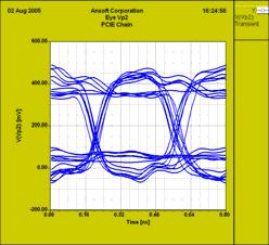
26 Allows Rapid What if Analyses All components "Active"


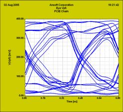
27 Allows Rapid What if Analyses Connector In In Circuit Connector "Bypassed" The connector has the largest effect on closing the eye

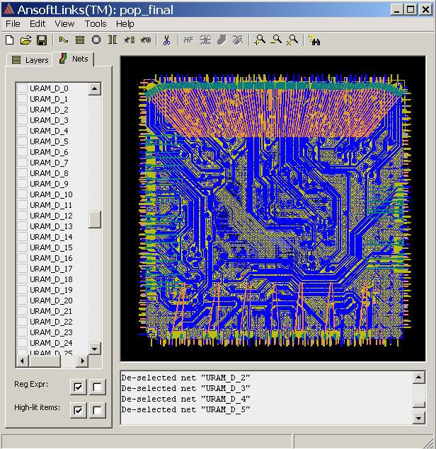
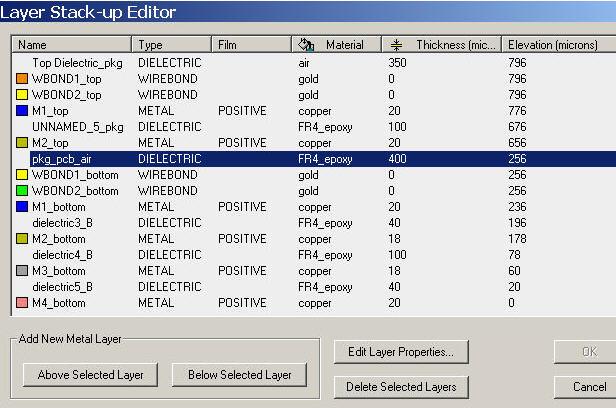
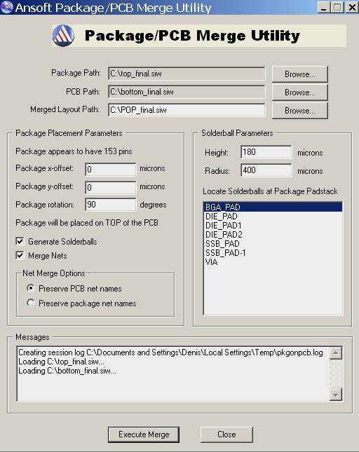
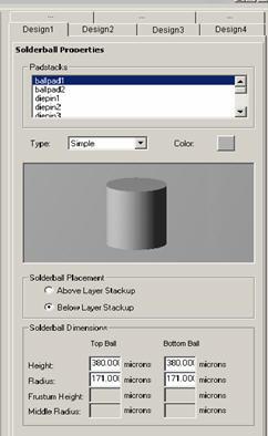
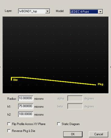
28 Package/Package Merge Utility


29 Package on Package/View
Enabling SI Productivity Part 2. Venkatesh Seetharam Aaron Edwards
 Enabling SI Productivity Part 2 Venkatesh Seetharam Aaron Edwards 1 Problem Statement SI engineers use simulation software to squeeze the most performance out of their design. They will tend to focus on
Package on Board Simulation with 3-D Electromagnetic Simulation
 White Paper Package on Board Simulation with 3-D Electromagnetic Simulation For many years, designers have taken into account the effect of package parasitics in simulation, from using simple first-order
Optimization of Modern Memory
 System Design, Verificationand and Optimization of Modern Memory Interfaces (DDR3) Santa Clara, Aug 23 rd 2011 Robert Myoung Sr. Application Engineer 1 Agenda Introduction ECAD Geometry Translation SI/PI
HFSS Solver-On-Demand for Package and PCB Characterization Using Cadence Greg Pitner
 HFSS Solver-On-Demand for Package and PCB Characterization Using Cadence Greg Pitner 1 ANSYS, Inc. September 14, Problem Statement Usually SI engineers extract only the package or the pcb due to the trade-offs
HFSS Solver On Demand for Package and PCB Characterization Using Cadence. Greg Pitner
 HFSS Solver On Demand for Package and PCB Characterization Using Cadence Greg Pitner 1 Problem Statement Usually SI engineers extract only the package or the pcb due to the trade offs between capacity
Electromagnetics. R14 Update. Greg Pitner ANSYS, Inc. February 24, 2012
 Electromagnetics R14 Update Greg Pitner 1 HFSS Version 14 2 HFSS Overview Advanced Integrated Solver Technologies Finite Arrays with Domain Decomposition Hybrid solving: FEBI, IE Regions Physical Optics
Modern Memory Interfaces (DDR3) Design with ANSYS Virtual Prototype approach
 Design with ANSYS Virtual Prototype approach") Modern Memory Interfaces (DDR3) Design with ANSYS Virtual Prototype approach 1 ANSYS, Inc. Proprietary 2012 ANSYS, Inc. November 14, 2012 1-1 Agenda DDR Design Challenges How does simulation solve these
Modern Memory Interfaces (DDR3) Design with ANSYS Virtual Prototype approach 1 ANSYS, Inc. Proprietary 2012 ANSYS, Inc. November 14, 2012 1-1 Agenda DDR Design Challenges How does simulation solve these
Allegro Sigrity SI Streamlining the creation of high-speed interconnect on digital PCBs and IC packages
 Streamlining the creation of high-speed interconnect on digital PCBs and IC packages The Cadence Allegro Sigrity signal integrity (SI) integrated high-speed design and analysis environment streamlines
A Modular Platform for Accurate Multi- Gigabit Serial Channel Validation
 A Modular Platform for Accurate Multi- Gigabit Serial Channel Validation Presenter: Andrew Byers Ansoft Corporation High Performance Electronics: Technical Challenges Faster data rates in increasingly
Electrical optimization and simulation of your PCB design
 Electrical optimization and simulation of your PCB design Steve Gascoigne Senior Consultant at Mentor Graphics Zagreb, 10. lipnja 2015. Copyright CADCAM Group 2015 The Challenge of Validating a Design..
HFSS 14 Update for SI and RF Applications Markus Kopp Product Manager, Electronics ANSYS, Inc.
 HFSS 14 Update for SI and RF Applications Markus Kopp Product Manager, Electronics ANSYS, Inc. 1 ANSYS, Inc. September 21, Advanced Solvers: Finite Arrays with DDM 2 ANSYS, Inc. September 21, Finite Arrays
Advanced SI Analysis Layout Driven Assembly. Tom MacDonald RF/SI Applications Engineer II
 Advanced SI Analysis Layout Driven Assembly 1 Tom MacDonald RF/SI Applications Engineer II Abstract As the voracious appetite for technology continually grows, so too does the need for fast turn around
SEAM-RA/SEAF-RA Series Final Inch Designs in PCI Express Applications Generation GT/s
 SEAM-RA/SEAF-RA Series Final Inch Designs in PCI Express Applications Generation 3-8.0 GT/s Copyrights and Trademarks Copyright 2011 Samtec, Inc. Developed in conjunction with Teraspeed Consulting Group
Application Note. PCIE-EM Series Final Inch Designs in PCI Express Applications Generation GT/s
 PCIE-EM Series Final Inch Designs in PCI Express Applications Generation 3-8.0 GT/s Copyrights and Trademarks Copyright 2015, Inc. COPYRIGHTS, TRADEMARKS, and PATENTS Final Inch is a trademark of, Inc.
Board Design Guidelines for PCI Express Architecture
 Board Design Guidelines for PCI Express Architecture Cliff Lee Staff Engineer Intel Corporation Member, PCI Express Electrical and Card WGs The facts, techniques and applications presented by the following
Realize Your Product Promise. DesignerRF
 Realize Your Product Promise DesignerRF Four-element antenna array showing current distribution and far-field gain, created in DesignerRF using layout editor and solved via HFSS with Solver on Demand technology
Application Note. PCIE-RA Series Final Inch Designs in PCI Express Applications Generation GT/s
 PCIE-RA Series Final Inch Designs in PCI Express Applications Generation 3-8.0 GT/s Copyrights and Trademarks Copyright 2012, Inc. COPYRIGHTS, TRADEMARKS, and PATENTS Final Inch is a trademark of, Inc.
ANSYS HFSS: Layout Driven Assembly in ANSYS Electronics Desktop
 Application Brief ANSYS HFSS: Layout Driven Assembly The ANSYS Electronics Desktop (AEDT) is an integrated environment with an easy-to-use interface that provides a streamlined workflow between ANSYS EM
What s New in HyperLynx 8.0
 What s New in HyperLynx 8.0 Copyright Mentor Graphics Corporation 2009 All Rights Reserved. Mentor Graphics, Board Station XE Flow, ViewDraw, Falcon Framework, IdeaStation, ICX and Tau are registered trademarks
Integrating ADS into a High Speed Package Design Process
 Integrating ADS into a High Speed Package Design Process Page 1 Group/Presentation Title Agilent Restricted Month ##, 200X Agenda High Speed SERDES Package Design Requirements Performance Factor and Design
PCIEC PCI Express Jumper High Speed Designs in PCI Express Applications Generation GT/s
 PCIEC PCI Express Jumper High Speed Designs in PCI Express Applications Generation 3-8.0 GT/s Mated with PCIE-RA Series PCB Connectors Copyrights and Trademarks Copyright 2015, Inc. COPYRIGHTS, TRADEMARKS,
Model Connection Protocol extensions for Mixed Signal SiP
 Model Connection Protocol extensions for Mixed Signal SiP Taranjit Kukal (kukal@cadence.com) Dr. Wenliang Dai (wldai@cadence.com) Brad Brim (bradb@sigrity.com) Presented by: Yukio Masuko Cadence Note:
An Innovative Simulation Workflow for Debugging High-Speed Digital Designs using Jitter Separation
 An Innovative Simulation Workflow for Debugging High-Speed Digital Designs using Jitter Separation C. Chastang, A. Amédéo V. Poisson, P. Grison, F. Demuynck C. Gautier, F. Costa Thales Communications &
Using Sonnet in a Cadence Virtuoso Design Flow
 Using Sonnet in a Cadence Virtuoso Design Flow Purpose of this document: This document describes the Sonnet plug-in integration for the Cadence Virtuoso design flow, for silicon accurate EM modelling of
QUEST 3D RLCG Extraction Depending on Frequency. RF Structures Parasitic Extractor
 QUEST 3D RLCG Extraction Depending on Frequency RF Structures Parasitic Extractor Introduction Type of Simulation Inputs / Outputs Graphical Interface Technology Process Layout Field Solver Output DOE
Large-Scale Full-Wave Simulation
 Large-Scale Full-Wave Simulation Sharad Kapur and David Long Integrand Software, Inc. Areas of interest Consistent trends in IC design Increasing operating frequencies Modeling of passive structures (components,
HFSS for ECAD: Package Modeling, MMIC and on-die extraction
 HFSS for ECAD: Package Modeling, MMIC and on-die extraction Alain Michel Technical Director, Europe 2010 ANSYS, Inc. All rights reserved. 1 ANSYS, Inc. Proprietary Agenda Introduction HFSS integrated Solver
RiseUp RU8-DP-DV Series 19mm Stack Height Final Inch Designs in PCI Express Applications. Revision Date: March 18, 2005
 RiseUp RU8-DP-DV Series 19mm Stack Height Final Inch Designs in PCI Express Applications Revision Date: March 18, 2005 Copyrights and Trademarks Copyright 2005 Samtec, Inc. Developed in conjunction with
Simulation and Modeling for Signal Integrity and EMC
 Simulation and Modeling for Signal Integrity and EMC Lynne Green Sr. Member of Consulting Staff Cadence Design Systems, Inc. 320 120th Ave NE Bellevue, WA 98005 USA (425) 990-1288 http://www.cadence.com
Q Pairs QTE/QSE-DP Final Inch Designs In PCI Express Applications 16 mm Stack Height
 Application Note Q Pairs QTE/QSE-DP Final Inch Designs In PCI Express Applications 16 mm Stack Height Copyrights and Trademarks Copyright 2004 Samtec, Inc. Developed in conjunction with Teraspeed Consulting
A Proposal for Developing S2IBISv3
 A Proposal for Developing S2IBISv3 Paul Franzon Michael Steer Automated Design Tools for Integrated Mixed Signal Microsystems (NeoCAD) Outline Background DARPA Program NeoCad Program Objectives Program
Implementing Multi-Gigabit Serial Links in a System of PCBs
 Implementing Multi-Gigabit Serial Links in a System of PCBs Donald Telian April 2002 rev. 1.2 About the Author Donald Telian Technologist, Cadence Design Systems Donald has been involved in high-speed
Explore your design space including IBIS AMI models with Advanced Channel Simulation
 Explore your design space including IBIS AMI models with Advanced Channel Simulation Heidi Barnes Vincent Poisson Presenter: May, 2013 Agenda How good is my PHY? Channel Simulation Options Spice (Circuit
Ansys Designer RF Training Lecture 2: Introduction to the Designer GUI
 Ansys Designer RF Solutions for RF/Microwave Component and System Design 7. 0 Release Ansys Designer RF Training Lecture 2: Introduction to the Designer GUI Ansoft Designer Desktop Menu bar Toolbars Schematic
Proposal for SAS 2.x Specification to Enable Support for Active Cables
 08-052r2 Proposal for SAS 2.x Specification to Enable Support for Active Cables Gourgen Oganessyan QUELLAN March 7, 2008 Introduction Inclusion of active cable interconnect option into the SAS specification
designs with signals operating in the multi-gigahertz (MGH) frequency range. It
 frequency range. It") DATASHEET ALLEGRO PCB SI GXL Cadence Allegro PCB SI GXL provides a virtual prototyping environment for designs with signals operating in the multi-gigahertz (MGH) frequency range. It offers a completely
DATASHEET ALLEGRO PCB SI GXL Cadence Allegro PCB SI GXL provides a virtual prototyping environment for designs with signals operating in the multi-gigahertz (MGH) frequency range. It offers a completely
Introducing Virtuoso RF Designer (RFD) For RFIC Designs
 For RFIC Designs") A seminar on Cadence Virtuoso RF Designer is scheduled for March 5, 2008. To know more, write to Brajesh Heda at brajesh@cadence.com Introducing Virtuoso RF Designer (RFD) For RFIC Designs Introduction
A seminar on Cadence Virtuoso RF Designer is scheduled for March 5, 2008. To know more, write to Brajesh Heda at brajesh@cadence.com Introducing Virtuoso RF Designer (RFD) For RFIC Designs Introduction
Optimum Placement of Decoupling Capacitors on Packages and Printed Circuit Boards Under the Guidance of Electromagnetic Field Simulation
 Optimum Placement of Decoupling Capacitors on Packages and Printed Circuit Boards Under the Guidance of Electromagnetic Field Simulation Yuzhe Chen, Zhaoqing Chen and Jiayuan Fang Department of Electrical
PI2EQX6874ZFE 4-lane SAS/SATA ReDriver Application Information
 Contents General Introduction How to use pin strap and I2C control External Components Requirement Layout Design Guide Power Supply Bypassing Power Supply Sequencing Equalization Setting Output Swing Setting
EM Analysis of High Frequency Printed Circuit Boards. Dr.-Ing. Volker Mühlhaus
 EM Analysis of High Frequency Printed Circuit Boards Dr.-Ing. Volker Mühlhaus volker@muehlhaus.com Agenda EM tools overview When to use EM analysis Application examples: Filters The importance of meshing
QPairs QTE/QSE-DP Multi-connector Stack Designs In PCI Express Applications 16 mm Connector Stack Height REVISION DATE: OCTOBER 13, 2004
 Application Note QPairs QTE/QSE-DP Multi-connector Stack Designs In PCI Express Applications 16 mm Connector Stack Height REVISION DATE: OCTOBER 13, 2004 Copyrights and Trademarks Copyright 2004 Samtec,
O N C A D E N C E V I R T U O S O. CHEN, Jason Application Engineer, Keysight Technologies
 O N C A D E N C E V I R T U O S O CHEN, Jason 2018.05.08 Application Engineer, Keysight Technologies Introduction to Momentum Momentum Features for RFIC Design Circuit/EM Cosimulation Flow on Cadence Virtuoso
High-Speed DDR4 Memory Designs and Power Integrity Analysis
 High-Speed DDR4 Memory Designs and Power Integrity Analysis Cuong Nguyen Field Application Engineer cuong@edadirect.com www.edadirect.com 2014 1 PCB Complexity is Accelerating Use of Advanced Technologies
I N T E R C O N N E C T A P P L I C A T I O N N O T E. Advanced Mezzanine Card (AMC) Connector Routing. Report # 26GC011-1 September 21 st, 2006 v1.
 Connector Routing. Report # 26GC011-1 September 21 st, 2006 v1.") I N T E R C O N N E C T A P P L I C A T I O N N O T E Advanced Mezzanine Card (AMC) Connector Routing Report # 26GC011-1 September 21 st, 2006 v1.0 Advanced Mezzanine Card (AMC) Connector Copyright 2006
I N T E R C O N N E C T A P P L I C A T I O N N O T E Advanced Mezzanine Card (AMC) Connector Routing Report # 26GC011-1 September 21 st, 2006 v1.0 Advanced Mezzanine Card (AMC) Connector Copyright 2006
PI2EQX6804-ANJE Four-lane SAS/SATA ReDriver Application Information May 13, 2011
 Contents General Introduction How to use pin strap and I2C control External Components Requirement Layout Design Guide Power Supply Bypassing Power Supply Sequencing Equalization Setting Output Swing Setting
Genesys 2012 Tutorial - Using Momentum Analysis for Microwave Planar Circuits
 Genesys 2012 Tutorial - Using Momentum Analysis for Microwave Planar Circuits Create the following schematics in Figure 1 with Genesys s schematic editor, which depicts two sections of a cascaded microstrip
89HPES24T3G2 Hardware Design Guide
 89H Hardware Design Guide Notes Introduction This document provides system design guidelines for IDT 89H PCI Express (PCIe ) 2. base specification compliant switch device. The letters "G2" within the device
I N T E R C O N N E C T A P P L I C A T I O N N O T E. STRADA Whisper 4.5mm Connector Enhanced Backplane and Daughtercard Footprint Routing Guide
 I N T E R C O N N E C T A P P L I C A T I O N N O T E STRADA Whisper 4.5mm Connector Enhanced Backplane and Daughtercard Footprint Routing Guide Report # 32GC001 01/26/2015 Rev 3.0 STRADA Whisper Connector
Modeling of Connector to PCB Interfaces. CST User Group Meeting, September 14, 2007 Thomas Gneiting, AdMOS GmbH
 Modeling of Connector to PCB Interfaces CST User Group Meeting, September 14, 2007 Thomas Gneiting, AdMOS GmbH thomas.gneiting@admos.de Table of Content Introduction Parametric CST model of connector to
ANSYS, Inc. March 3, 2016 PCB 板极电热耦合分析及对电子设备热设计的影响
 1 2015 ANSYS, Inc. March 3, 2016 PCB 板极电热耦合分析及对电子设备热设计的影响 Printed Circuit Board Reliability Real world operating conditions = Multiphysics environment Electrical Reliability Power and Signal Integrity
Q2 QMS/QFS 16mm Stack Height Final Inch Designs In PCI Express Applications Generation Gbps. Revision Date: February 13, 2009
 Q2 QMS/QFS 16mm Stack Height Final Inch Designs In PCI Express Applications Generation 2 5.0 Gbps Revision Date: February 13, 2009 Copyrights and Trademarks Copyright 2009 Samtec, Inc. Developed in conjunction
Outline. Darren Wang ADS Momentum P2
 Outline Momentum Basics: Microstrip Meander Line Momentum RF Mode: RFIC Launch Designing with Momentum: Via Fed Patch Antenna Momentum Techniques: 3dB Splitter Look-alike Momentum Optimization: 3 GHz Band
An Overview of High-Speed Serial Bus Simulation Technologies
 An Overview of High-Speed Serial Bus Simulation Technologies Asian IBIS Summit, Beijing, China September 11, 27.25.2.15.1.5 -.5 -.1 Arpad Muranyi arpad_muranyi@mentor.com Vladimir Dmitriev-Zdorov -.15
Tsi384 Board Design Guidelines
 Tsi384 Board Design Guidelines September 2009 6024 Silver Creek Valley Road, San Jose, California 95138 Telephone: (800) 345-7015 (408) 284-8200 FAX: (408) 284-2775 Printed in U.S.A. 2009, Inc. GENERAL
TABLE OF CONTENTS 1.0 PURPOSE INTRODUCTION ESD CHECKS THROUGHOUT IC DESIGN FLOW... 2
 TABLE OF CONTENTS 1.0 PURPOSE... 1 2.0 INTRODUCTION... 1 3.0 ESD CHECKS THROUGHOUT IC DESIGN FLOW... 2 3.1 PRODUCT DEFINITION PHASE... 3 3.2 CHIP ARCHITECTURE PHASE... 4 3.3 MODULE AND FULL IC DESIGN PHASE...
Advances in Measurement Based Transient Simulation
 Time Domain Simulation in ADS, Slide - 1 Advances in Measurement Based Transient Simulation Presented by GigaTest Labs Gary Otonari and Orlando Bell March, 2008 1 Time Domain Simulation in ADS, Slide -
Proposal for SAS 2.x Specification to Enable Support for Active Cables
 08-052r5 Proposal for SAS 2.x Specification to Enable Support for Active Cables Gourgen Oganessyan QUELLAN June 5, 2008 Introduction Inclusion of active cable interconnect option into the SAS specification
IDT PEB383 QFP Board Design Guidelines
 IDT PEB383 QFP Board Design Guidelines February 2010 6024 Silver Creek Valley Road, San Jose, California 95138 Telephone: (800) 345-7015 (408) 284-8200 FAX: (408) 284-2775 Printed in U.S.A. 2009 GENERAL
Tsi381 Board Design Guidelines
 Tsi381 Board Design Guidelines September 2009 6024 Silver Creek Valley Road, San Jose, California 95138 Telephone: (800) 345-7015 (408) 284-8200 FAX: (408) 284-2775 Printed in U.S.A. 2009, Inc. GENERAL
APDS Wizard v4 for Nexxim/Designer 4.0 Specially optimized for DDR2/3 SI. Ansoft Korea Team
 APDS Wizard v4 for Nexxim/Designer 4.0 Specially optimized for DDR2/3 SI Ansoft Korea Team APDS Wizard v4 All-Renewed, Enhanced Wizard. Version 4 means this new wizard would work with Designer/Nexxim v4
EECE 615: High-Frequency Design Techniques
 Department of Electrical and Computer Engineering EECE 615: High-Frequency Design Techniques Prerequisites: EECE 417, PHYS 204C Required for all MSEE majors Catalog Description:Study of the problems associated
ASIX USB-to-LAN Applications Layout Guide
 ASIX USB-to-LAN Applications Revision 1.0 Dec. 11th, 2007 1 Revision Date Description 1.0 2007/12/11 New release. ASIX USB-to-LAN Applications Revision History 2 Content 1. Introduction...4 2. 4-Layer
Baseband IC Design Kits for Rapid System Realization
 Baseband IC Design Kits for Rapid System Realization Lanbing Chen Cadence Design Systems Engineering Director John Rowland Spreadtrum Communications SVP of Hardware Engineering Agenda How to Speed Up IC
Optimal Management of System Clock Networks
 Optimal Management of System Networks 2002 Introduction System Management Is More Challenging No Longer One Synchronous per System or Card Must Design Source-Synchronous or CDR Interfaces with Multiple
Introduction Electrical Considerations Data Transfer Synchronization Bus Arbitration VME Bus Local Buses PCI Bus PCI Bus Variants Serial Buses
 Introduction Electrical Considerations Data Transfer Synchronization Bus Arbitration VME Bus Local Buses PCI Bus PCI Bus Variants Serial Buses 1 Most of the integrated I/O subsystems are connected to the
REV CHANGE DESCRIPTION NAME DATE. A Release B Increased +1.2V Capacitor Value & VDD12A Cap Requirement
 REV CHANGE DESCRIPTION NAME DATE A Release 1-20-16 B Increased +1.2V Capacitor Value & VDD12A Cap Requirement 1-16-17 Any assistance, services, comments, information, or suggestions provided by Microchip
Advanced Modeling and Simulation Strategies for Power Integrity in High-Speed Designs
 Advanced Modeling and Simulation Strategies for Power Integrity in High-Speed Designs Ramachandra Achar Carleton University 5170ME, Dept. of Electronics Ottawa, Ont, Canada K1S 5B6 *Email: achar@doe.carleton.ca;
Agilent Bead Probe Technology
 Agilent Bead Probe Technology Page 1 Abstract Lead-free, shrinking geometries, new packages and high-speed signaling present new challenges for ICT. The impact will be more defects, loss of access, lower
HFSS 14 Update for SI and RF Applications. Presenter: Senior Application Engineer Jeff Tharp, Ph.D.
 HFSS 14 Update for SI and RF Applications Presenter: Senior Application Engineer Jeff Tharp, Ph.D. 1 Overview Advanced Integrated Solver Technologies Finite Arrays with Domain Decomposition Hybrid solving
Signal Integrity Comparisons Between Stratix II and Virtex-4 FPGAs
 White Paper Introduction Signal Integrity Comparisons Between Stratix II and Virtex-4 FPGAs Signal integrity has become a critical issue in the design of high-speed systems. Poor signal integrity can mean
ALLEGRO PCB SI 630 DATASHEET VIRTUAL PROTOTYPING ENVIRONMENT FOR DESIGNS WITH MULTI-GIGAHERTZ SIGNALS THE ALLEGRO SYSTEM INTERCONNECT DESIGN PLATFORM
 DATASHEET ALLEGRO PCB SI 630 VIRTUAL PROTOTYPING ENVIRONMENT FOR DESIGNS WITH MULTI-GIGAHERTZ SIGNALS Cadence Allegro PCB SI 630 a key PCB Signal Integrity tool within the Allegro system interconnect design
3D EM Simulation in the Design Flow of High-Speed Multi-Pin Connectors
 3D EM Simulation in the Design Flow of High-Speed Multi-Pin Connectors Application and Simulation courtesy of Thomas Gneiting, AdMOS GmbH, Frickenhausen, Germany. This article describes the design flow
THREE THINGS TO CONSIDER WHEN DESIGNING ELECTRONIC PRODUCTS WITH HIGH-SPEED CONSTRAINTS BY: PATRICK CARRIER, MENTOR GRAPHICS CORP.
 THREE THINGS TO CONSIDER WHEN DESIGNING ELECTRONIC PRODUCTS WITH HIGH-SPEED CONSTRAINTS BY: PATRICK CARRIER, MENTOR GRAPHICS CORP. P A D S W H I T E P A P E R w w w. p a d s. c o m INTRODUCTION Designing
High Speed and High Power Connector Design
 High Speed and High Power Connector Design Taiwan User Conference 2014 Introduction High speed connector: Electrically small Using differential signaling Data rate >100Mbps High power connector: Static
AWR. White Paper. Exactly How Electromagnetic Should Be Part of a Design Flow! introduction
 Extract Flow introduction Modern RF/microwave design flows make extensive use of electromagnetic (EM) analysis in many ways, and its co-existence and concurrency with circuit design and analysis can not
Homework 6: Printed Circuit Board Layout Design Narrative
 Homework 6: Printed Circuit Board Layout Design Narrative Team Code Name: Home Kinection Group No. 1 Team Member Completing This Homework: Stephen Larew E-mail Address of Team Member: sglarew @ purdue.edu
W5100 Layout Guide version 1.0
 version 1.0 2009 WIZnet Co., Inc. All Rights Reserved. For more information, visit our website at http://www.wiznet.co.kr Copyright 2009 WIZnet Co., Inc. All rights reserved. Table of Contents 1 Goal...
PEX 8505 Quick Start Hardware Design Guide
 PEX 8505 Quick Start Hardware Design Guide Version 1.0 November 2007 Website: http://www.plxtech.com Email: apps@plxtech.com Phone: 408 774-9060 800 759-3735 Fax: 408 774-2169 PLX Technology, Inc. retains
Virtuoso Custom Design Platform GXL. Open Database. PDKs. Constraint Management. Customer IP
 Virtuoso Custom Design Platform GL The Cadence Virtuoso custom design platform is the industry s leading design system for complete front-to-back analog, RF, mixed-signal, and custom digital design. The
Signal Integrity Analysis for 56G-PAM4 Channel of 400G Switch
 Signal Integrity Analysis for 56G-PAM4 Channel of 400G Switch Sophia Feng/Vincent Wen of Celestica sopfeng@celestica.com Asian IBIS Summit Shanghai, PRC November 13, 2017 Agenda Background 200GBASE-KR4
New Technologies in CST STUDIO SUITE CST COMPUTER SIMULATION TECHNOLOGY
 New Technologies in CST STUDIO SUITE 2016 Outline Design Tools & Modeling Antenna Magus Filter Designer 2D/3D Modeling 3D EM Solver Technology Cable / Circuit / PCB Systems Multiphysics CST Design Tools
Understanding 3M Ultra Hard Metric (UHM) Connectors
 Connectors") 3M Electronic Solutions Division 3MUHMWEBID_100809 Understanding 3M Ultra Hard Metric (UHM) Connectors Enabling performance of next generation 2 mm Hard Metric systems 3M Electronic Solutions Division
3M Electronic Solutions Division 3MUHMWEBID_100809 Understanding 3M Ultra Hard Metric (UHM) Connectors Enabling performance of next generation 2 mm Hard Metric systems 3M Electronic Solutions Division
A Practical Approach to Preventing Simultaneous Switching Noise and Ground Bounce Problems in IO Rings
 A Practical Approach to Preventing Simultaneous Switching Noise and Ground Bounce Problems in IO Rings Dr. Osman Ersed Akcasu, Jerry Tallinger, Kerem Akcasu OEA International, Inc. 155 East Main Avenue,
Advances in 3D Simulations of Chip/Package/PCB Co-Design
 Advances in 3D Simulations of Chip/Package/PCB Co-Design Richard Sjiariel, CST AG Co-design environment Signal Integrity and timing Thermal analysis and stress Power Integrity and noise analysis EMC/EMI
XSFP-T-RJ Base-T Copper SFP Transceiver
 Product Overview The electrical Small Form Factor Pluggable (SFP) transceiver module is specifically designed for the high performance integrated full duplex data link at 1.25Gbps over four pair Category
GIGALIGHT CXP-CXP Active Optical Cable GCX-DO151G-XXXC
 GIGALIGHT CXP-CXP Active Optical Cable GCX-DO151G-XXXC Features Full duplex 12 channel 850nm parallel active optical cable Transmission data rate up to 12.5Gbit/s per channel Hot pluggable electrical interface
HIPEX Full-Chip Parasitic Extraction. Summer 2004 Status
 HIPEX Full-Chip Parasitic Extraction Summer 2004 Status What is HIPEX? HIPEX Full-Chip Parasitic Extraction products perform 3D-accurate and 2D-fast extraction of parasitic capacitors and resistors from
AXIEM EM Simulation/Verification of a Cadence Allegro PCB
 Application Example AXIEM EM Simulation/Verification of a Cadence Allegro PCB Overview This application example outlines the electromagnetic (EM) simulation and verification flow that exists between Cadence
MDI for 4x25G Copper and Fiber Optic IO. Quadra (CFP4 proposal) Connector System
 Connector System") MDI for 4x25G Copper and Fiber Optic IO Quadra (CFP4 proposal) Connector System Nov 7, 2011 Nathan Tracy, TE Connectivity Tom Palkert, Molex 4x25Gb/s MDI Potential Requirements Critical Needs: Excellent
MDI for 4x25G Copper and Fiber Optic IO Quadra (CFP4 proposal) Connector System Nov 7, 2011 Nathan Tracy, TE Connectivity Tom Palkert, Molex 4x25Gb/s MDI Potential Requirements Critical Needs: Excellent
CENG 4480 Lecture 11: PCB
 CENG 4480 Lecture 11: PCB Bei Yu Reference: Chapter 5 of Ground Planes and Layer Stacking High speed digital design by Johnson and Graham 1 Introduction What is a PCB Why we need one? For large scale production/repeatable
Simulation Strategies for Massively Parallel Supercomputer Design
 Simulation Strategies for Massively Parallel Supercomputer Design Authored by: Ansoft Corporation Special Thanks to: Cray Presentation #2 Ansoft 2003 / Global Seminars: Delivering Performance Introduction
Hipex Full-Chip Parasitic Extraction
 What is Hipex? products perform 3D-accurate and 2D-fast extraction of parasitic capacitors and resistors from hierarchical layouts into hierarchical transistor-level netlists using nanometer process technology
SV3C DPRX MIPI D-PHY Analyzer. Data Sheet
 SV3C DPRX MIPI D-PHY Analyzer Data Sheet Table of Contents Table of Contents Table of Contents... 1 List of Figures... 2 List of Tables... 2 Introduction... 3 Overview... 3 Key Benefits... 3 Applications...
AN INTRODUCTION TO HYPERLYNX SI/PI TECHNOLOGY
 AN INTRODUCTION TO HYPERLYNX SI/PI TECHNOLOGY BY STEVE KAUFER, MENTOR H I G H S P E E D D E S I G N W H I T E P A P E R OVERVIEW Digital designers are now required to make the leap from time domain to
New Enhanced Possibilities of Netlist Comparison in Guardian LVS
 Application Note New Enhanced Possibilities of Netlist Comparison in Guardian LVS 1. Introduction The Guardian LVS (Layout versus Schematic) netlist comparison tool compares two SPICE netlists. One of
Designing and Verifying Future High Speed Busses
 Designing and Verifying Future High Speed Busses Perry Keller Agilent Technologies Gregg Buzard December 12, 2000 Agenda Bus Technology Trends and Challenges Making the transition: Design and Test of DDR
High-Speed Layout Guidelines for Reducing EMI for LVDS SerDes Designs. I.K. Anyiam
 High-Speed Layout Guidelines for Reducing EMI for LVDS SerDes Designs I.K. Anyiam 1 Introduction LVDS SerDes helps to reduce radiated emissions, but does not completely eliminate them EMI prevention must
HMC7545AxLP Gbps 4-Channel Asynchronous Signal Conditioner Evaluation Board (EVB) User Guide
 User Guide") HMC7545AxLP47 14.2 Gbps 4-Channel Asynchronous Signal Conditioner Evaluation Board (EVB) User Guide User Guide Part # ECN# CP140238 Hittite Microwave Corporation 2 Elizabeth Dr Chelmsford, MA 01824 United
HMC7545AxLP47 14.2 Gbps 4-Channel Asynchronous Signal Conditioner Evaluation Board (EVB) User Guide User Guide Part # ECN# CP140238 Hittite Microwave Corporation 2 Elizabeth Dr Chelmsford, MA 01824 United
MIPI D-PHY REFERENCE TERMINATION BOARD (RTB) OVERVIEW AND DATASHEET
 OVERVIEW AND DATASHEET") The InterOperability Laboratory MIPI D-PHY REFERENCE TERMINATION BOARD (RTB) OVERVIEW AND DATASHEET Abstract: This document serves as the primary documentation for the MIPI D-PHY Reference Termination
The InterOperability Laboratory MIPI D-PHY REFERENCE TERMINATION BOARD (RTB) OVERVIEW AND DATASHEET Abstract: This document serves as the primary documentation for the MIPI D-PHY Reference Termination
Proposal for SAS 2.1 Specification to Enable Support for Active Cables
 08-358r3 Proposal for SAS 2.1 Specification to Enable Support for Active Cables Revision 13 Gourgen Oganessyan QUELLAN January 12, 2009 Introduction Inclusion of active cable interconnect option into the