Embedded Memory Alternatives
|
|
|
- Brian Cunningham
- 5 years ago
- Views:
Transcription

1 EE241 - Spring 2005 Advanced Digital Integrated Circuits Lecture 26: Embedded Memory - Flash Slides Courtesy of Randy McKee, TI Embedded Memory Alternatives Courtesy Randy McKee, TI 2 1
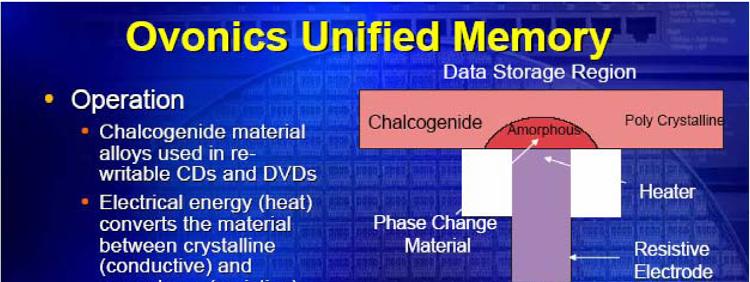


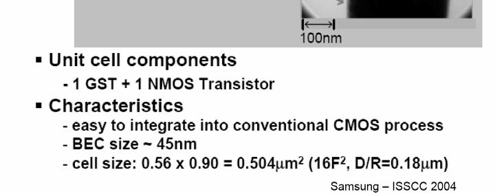
2 3 4 2
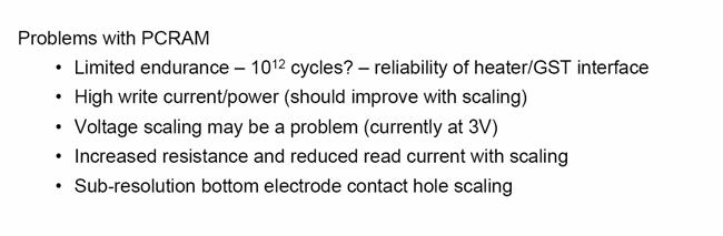
3 5 SRAM 3


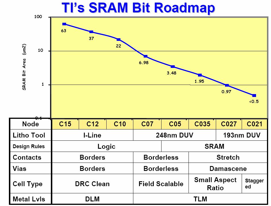
4 90 nm SRAM cell sizes 7 The art of making small cells 8 4
5 9 10 5
6 SRAM Yield Limitations Read Stability Cell can flip due to increase in the 0 storage node above the trip voltage of the other inverter during a read. Hold Stability Data retention current not able to compensate the leakage currents. Access Time Time required to produce a pre-specified V between the bit lines is higher than the maximum tolerable limit. Write Stability 1 Storage node may not be reduced below the trip point of the other inverter before WL is discharged. Mukhopadhyay et al, Read Stability F1( VL) = V F2( V L S = F2( V S) = V L L + c L S + c S) F1( VL) Bhavnagarwala et al, 2001 F1( VL) F2( VL SNM) = 0 VL VL 12 6
7 Hold Stability Similar to Read Stability analysis without access transistor. PR must provide enough leakage to compensate for leakage in NMOS pull-down and access transistors. 13 Read Access Must provide V between the bit lines within maximum tolerable time limit. Limited to floating bit-line implementation with voltage sensing amplifiers. Sum BL currents and integrate. T ACCESS = VDD VBL, R VMIN VDD C dv IBL, L BL, L BL, L = VDD VBL, R VDD C dv IBL, R BL, R BL, R Mukhopadhyay et al,
 dvr )( VR) Iout( R) ( VR) < T WL for write stability.")
8 Write Stability Need V WRITE < V TRIP for writability. T WRITE VTRIP = VDD I in( R CR( VR) dvr )( VR) Iout( R) ( VR) < T WL for write stability. Mukhopadhyay et al,
9

 20")
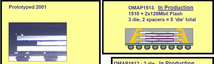

10 19 Some stacked solutions (TI) 20 10


11 21 Semiconductor Memory Trends From [Itoh01] 22 11
![Trends in Memory Cell Area From [Itoh01] 23 Flash](/docs-images/82/84759041/images/12-0.jpg "Memory Slides adapted from Ken Takeuchi, Toshiba")
12 Trends in Memory Cell Area From [Itoh01] 23 Flash Memory Slides adapted from Ken Takeuchi, Toshiba 12
13 Flash EEPROM Control gate Floating gate erasure n + source programming p- substrate Thin tunneling oxide n + drain Many other options 25 Basic Operations in a NOR Flash Memory Erase 26 13
14 Basic Operations in a NOR Flash Memory Write 27 Basic Operations in a NOR Flash Memory Read 28 14
15 History of Flash Memories PRESENT SanDisk-type SanDisk-type FLASH MEMORY Invention NANDtype ACEEtype X AND-type NAND-type AND-type File- Storage NOR-type NOR-type Split-gate-type X SST-type SST-type Code- Storage DiNOR-type DiNOR-type 29 Flash Memory Comparison - Code vs File Storage - Code Storage Applications Program storage for - Cellular Phone -DVD -Set TOP Box BIOS for - PC and peripherals Performance Important : High speed random access Byte programming Acceptable : Slow programming Slow erasing Type of Flash memory NOR Intel / Sharp AMD / Fujitsu / Toshiba DINOR Mitsubishi File Storage Small form factor card for - Digital Still Camera - Silicon Audio - PDA... etc Mass storage as - Silicon Disk Drive Important : High speed programming High speed erasing High speed serial read Acceptable : Slow random access NAND Toshiba / Samsung AND Hitachi SanDisk: NOR 30 15
16 Requirements for File Storage Memory Low Bit Cost <$.2/MByte High Density >256MByte High Speed Programming >6MByte/sec and Erasing <3msec/block High Speed Serial Read Low Power Consumption Good Program/Erase Endurance >1 million cycles 31 Cell Array Comparison NOR SanDisk AND NAND Bit line(metal) Bit line /Source line(metal) Word line(poly) Contact Erase gate(poly) Word line(poly) Word line(poly) Word line(poly) Source line (Diff. Layer) Sub Bit line (Diff. Layer) 10F 2 Unit Cell Unit Cell Unit Cell 9F 2 Unit Cell 8F 2 4F 2 Source line (Diff. Layer) Source line (Diff. Layer) Simplest wiring Smallest area 32 16
17 NAND Cell Array (Top view) Select transistor Word lines Active area STI Bit line contact Source line contact 33 NAND Cell Array (Cross sectional view) Word line A A A Bit line A Word line Select gate Source line 34 17
18 Cell Size Shrink by Self-Aligned STI LOCOS_NAND LOCOS_NAND :: 6F 6F+ 2 2 Floating Gate 3 Word Line STI_NAND STI_NAND :: 4F 4F+ 2 2 F Current F 35 NAND Cell Array (Cross sectional view) 2 nd floating gate Word line 1 st floating gate B B Word line STI Si B B 36 18
 Control")
19 NAND Cell Trend NOR-type Cell NAND-type Cell (Contactless) Self-Aligned STI Cell Self-Aligned STI Cell + Multi Level Cell 3.5F 2F 2F 2F 3F 3F Cell Size 10-11F 2 6-7F 2 4-5F F 2 Isolation LOCOS LOCOS SA-STI SA-STI 2F 2F Floating Gate Control Gate Floating Gate Control Gate LOCOS STI 37 NAND Flash Cell Size Trend 10 LOCOS SA-STI MLC 1 SA-STI Cell Size ( um 2 ) Control Gate Tunnel Oxide Floating Gate ONO LOCOS WSi 0.25um Multi Level Cell 0.1 Control Gate Floating Gate Tunnel Oxide ONO STI WSi 0.175um 0.13um 0.10um 0.01 Jan- Jan- Jan- Jan- Jan- Jan- Jan- Jan- Jan- Jan- Jan- Jan Start of Mass Production 38 19
20 That s all Folks Thanks for the fun semester. See you next Monday 39 20
Flash TOSHIBA TOSHIBA
 Flash VOLATILE Mobile Application Low Power SDRAM Pseudo SRAM High Speed Application embedded edram PLEDM FBC memory Low Power Low Power SRAM QDR SRAM DDR SRAM Sigma RAM FeRAM High Speed MRAM OUM Universal
ECE321 Electronics I
 ECE321 Electronics I Lecture 28: DRAM & Flash Memories Payman Zarkesh-Ha Office: ECE Bldg. 230B Office hours: Tuesday 2:00-3:00PM or by appointment E-mail: payman@ece.unm.edu Slide: 1 Review of Last Lecture
Advanced Information Storage 11
 Advanced Information Storage 11 Atsufumi Hirohata Department of Electronics 16:00 11/November/2013 Monday (P/L 002) Quick Review over the Last Lecture Shingled write recording : * Bit patterned media (BPM)
NAND Flash Memory. Jinkyu Jeong Computer Systems Laboratory Sungkyunkwan University
 NAND Flash Memory Jinkyu Jeong (Jinkyu@skku.edu) Computer Systems Laboratory Sungkyunkwan University http://csl.skku.edu ICE3028: Embedded Systems Design, Fall 2018, Jinkyu Jeong (jinkyu@skku.edu) Flash
EE141-Fall 2007 Digital Integrated Circuits. ROM and Flash. Announcements. Read-Only Memory Cells. Class Material. Semiconductor Memory Classification
 EE4-Fall 2007 igital Integrated Circuits Lecture 29 ROM, Flash, and RAM ROM and Flash 4 4 Announcements Final ec. 20 th Room TBA Final review sessions: Mon. ec. 7 th 3:30pm, 550 Cory Tues. ec. 7 th 3:30pm,
NAND Flash Memory: Basics, Key Scaling Challenges and Future Outlook. Pranav Kalavade Intel Corporation
 NAND Flash Memory: Basics, Key Scaling Challenges and Future Outlook Pranav Kalavade Intel Corporation pranav.kalavade@intel.com October 2012 Outline Flash Memory Product Trends Flash Memory Device Primer
+1 (479)
") Memory Courtesy of Dr. Daehyun Lim@WSU, Dr. Harris@HMC, Dr. Shmuel Wimer@BIU and Dr. Choi@PSU http://csce.uark.edu +1 (479) 575-6043 yrpeng@uark.edu Memory Arrays Memory Arrays Random Access Memory Serial
Memory Courtesy of Dr. Daehyun Lim@WSU, Dr. Harris@HMC, Dr. Shmuel Wimer@BIU and Dr. Choi@PSU http://csce.uark.edu +1 (479) 575-6043 yrpeng@uark.edu Memory Arrays Memory Arrays Random Access Memory Serial
Memory Design I. Array-Structured Memory Architecture. Professor Chris H. Kim. Dept. of ECE.
 Memory Design I Professor Chris H. Kim University of Minnesota Dept. of ECE chriskim@ece.umn.edu Array-Structured Memory Architecture 2 1 Semiconductor Memory Classification Read-Write Wi Memory Non-Volatile
Embedded System Application
 Laboratory Embedded System Application 4190.303C 2010 Spring Semester ROMs, Non-volatile and Flash Memories ELPL Naehyuck Chang Dept. of EECS/CSE Seoul National University naehyuck@snu.ac.kr Revisit Previous
Introduction to CMOS VLSI Design. Semiconductor Memory Harris and Weste, Chapter October 2018
 Introduction to CMOS VLSI Design Semiconductor Memory Harris and Weste, Chapter 12 25 October 2018 J. J. Nahas and P. M. Kogge Modified from slides by Jay Brockman 2008 [Including slides from Harris &
Memory Design I. Semiconductor Memory Classification. Read-Write Memories (RWM) Memory Scaling Trend. Memory Scaling Trend
 Memory Scaling Trend. Memory Scaling Trend") Array-Structured Memory Architecture Memory Design I Professor hris H. Kim University of Minnesota Dept. of EE chriskim@ece.umn.edu 2 Semiconductor Memory lassification Read-Write Memory Non-Volatile Read-Write
Array-Structured Memory Architecture Memory Design I Professor hris H. Kim University of Minnesota Dept. of EE chriskim@ece.umn.edu 2 Semiconductor Memory lassification Read-Write Memory Non-Volatile Read-Write
EE241 - Spring 2007 Advanced Digital Integrated Circuits. Announcements
 EE241 - Spring 2007 Advanced Digital Integrated Circuits Lecture 22: SRAM Announcements Homework #4 due today Final exam on May 8 in class Project presentations on May 3, 1-5pm 2 1 Class Material Last
NAND Flash: Where we are, where are we going?
 NAND Flash: Where we are, where are we going? Pranav Kalavade Intel Corporation Outline Introduction 3D NAND Floating Gate 3D NAND Technology CMOS Under Array Cell Characteristics Summary Cell Size [um
Flash ( p.531)
") Introduction to CMOS VLSI Design Flash (12.4.3.531) J. J. Nahas and P. M. Kogge Modified from slides by Jay Brockman 2008, 2015,2018 [Including slides from Harris & Weste, Ed 4, Adated from Mary Jane Irwin
Introduction to CMOS VLSI Design Flash (12.4.3.531) J. J. Nahas and P. M. Kogge Modified from slides by Jay Brockman 2008, 2015,2018 [Including slides from Harris & Weste, Ed 4, Adated from Mary Jane Irwin
ΔΙΑΛΕΞΗ 5: FPGA Programming Technologies (aka: how to connect/disconnect wires/gates)
") ΗΜΥ 408 ΨΗΦΙΑΚΟΣ ΣΧΕΔΙΑΣΜΟΣ ΜΕ FPGAs Χειμερινό Εξάμηνο 2018 ΔΙΑΛΕΞΗ 5: FPGA Programming Technologies (aka: how to connect/disconnect wires/gates) (ack: Jurriaan Schmitz, Semiconductor Components) ΧΑΡΗΣ
ΗΜΥ 408 ΨΗΦΙΑΚΟΣ ΣΧΕΔΙΑΣΜΟΣ ΜΕ FPGAs Χειμερινό Εξάμηνο 2018 ΔΙΑΛΕΞΗ 5: FPGA Programming Technologies (aka: how to connect/disconnect wires/gates) (ack: Jurriaan Schmitz, Semiconductor Components) ΧΑΡΗΣ
EECS 427 Lecture 17: Memory Reliability and Power Readings: 12.4,12.5. EECS 427 F09 Lecture Reminders
 EECS 427 Lecture 17: Memory Reliability and Power Readings: 12.4,12.5 1 Reminders Deadlines HW4 is due Tuesday 11/17 at 11:59 pm (email submission) CAD8 is due Saturday 11/21 at 11:59 pm Quiz 2 is on Wednesday
Advanced Digital Integrated Circuits. Lecture 9: SRAM. Announcements. Homework 1 due on Wednesday Quiz #1 next Monday, March 7
 EE241 - Spring 2011 Advanced Digital Integrated Circuits Lecture 9: SRAM Announcements Homework 1 due on Wednesday Quiz #1 next Monday, March 7 2 1 Outline Last lecture Variability This lecture SRAM 3
Advanced Digital Integrated Circuits. Lecture 9: SRAM. Announcements. Homework 1 due on Wednesday Quiz #1 next Monday, March 7
 EE24 - Spring 20 Advanced Digital Integrated Circuits Lecture 9: SRAM Announcements Homework due on Wednesday Quiz # next Monday, March 7 2 Outline Last lecture Variability This lecture SRAM 3 Practical
COMP3221: Microprocessors and. and Embedded Systems. Overview. Lecture 23: Memory Systems (I)
") COMP3221: Microprocessors and Embedded Systems Lecture 23: Memory Systems (I) Overview Memory System Hierarchy RAM, ROM, EPROM, EEPROM and FLASH http://www.cse.unsw.edu.au/~cs3221 Lecturer: Hui Wu Session
COMP3221: Microprocessors and Embedded Systems Lecture 23: Memory Systems (I) Overview Memory System Hierarchy RAM, ROM, EPROM, EEPROM and FLASH http://www.cse.unsw.edu.au/~cs3221 Lecturer: Hui Wu Session
Chapter 3 Semiconductor Memories. Jin-Fu Li Department of Electrical Engineering National Central University Jungli, Taiwan
 Chapter 3 Semiconductor Memories Jin-Fu Li Department of Electrical Engineering National Central University Jungli, Taiwan Outline Introduction Random Access Memories Content Addressable Memories Read
Memory Classification revisited. Slide 3
 Slide 1 Topics q Introduction to memory q SRAM : Basic memory element q Operations and modes of failure q Cell optimization q SRAM peripherals q Memory architecture and folding Slide 2 Memory Classification
Flash Memory. Gary J. Minden November 12, 2013
 Flash Memory Gary J. Minden November 12, 2013 1 Memory Types Static Random Access Memory (SRAM) Register File Cache Memory on Processor Dynamic Random Access Memory (DRAM, SDRAM) Disk Solid State Disk
Memory. Outline. ECEN454 Digital Integrated Circuit Design. Memory Arrays. SRAM Architecture DRAM. Serial Access Memories ROM
 ECEN454 Digital Integrated Circuit Design Memory ECEN 454 Memory Arrays SRAM Architecture SRAM Cell Decoders Column Circuitry Multiple Ports DRAM Outline Serial Access Memories ROM ECEN 454 12.2 1 Memory
CS311 Lecture 21: SRAM/DRAM/FLASH
 S 14 L21-1 2014 CS311 Lecture 21: SRAM/DRAM/FLASH DARM part based on ISCA 2002 tutorial DRAM: Architectures, Interfaces, and Systems by Bruce Jacob and David Wang Jangwoo Kim (POSTECH) Thomas Wenisch (University
Introduction to SRAM. Jasur Hanbaba
 Introduction to SRAM Jasur Hanbaba Outline Memory Arrays SRAM Architecture SRAM Cell Decoders Column Circuitry Non-volatile Memory Manufacturing Flow Memory Arrays Memory Arrays Random Access Memory Serial
Lecture 13: SRAM. Slides courtesy of Deming Chen. Slides based on the initial set from David Harris. 4th Ed.
 Lecture 13: SRAM Slides courtesy of Deming Chen Slides based on the initial set from David Harris CMOS VLSI Design Outline Memory Arrays SRAM Architecture SRAM Cell Decoders Column Circuitry Multiple Ports
Information Storage and Spintronics 10
 Information Storage and Spintronics 10 Atsufumi Hirohata Department of Electronic Engineering 09:00 Tuesday, 30/October/2018 (J/Q 004) Quick Review over the Last Lecture Flash memory : NAND-flash writing
Sense Amplifiers 6 T Cell. M PC is the precharge transistor whose purpose is to force the latch to operate at the unstable point.
 Announcements (Crude) notes for switching speed example from lecture last week posted. Schedule Final Project demo with TAs. Written project report to include written evaluation section. Send me suggestions
Flash Memories. Ramin Roosta Dept. of Computer Engineering. EE 595 EDA / ASIC Design Lab
 Flash Memories Ramin Roosta Dept. of Computer Engineering EE 595 EDA / ASIC Design Lab Content Non-volatile memories Flash applications Industry standards Architectures Main reliability issues New cells
Data Retention in MLC NAND Flash Memory: Characterization, Optimization, and Recovery
 Data Retention in MLC NAND Flash Memory: Characterization, Optimization, and Recovery Yu Cai, Yixin Luo, Erich F. Haratsch*, Ken Mai, Onur Mutlu Carnegie Mellon University, *LSI Corporation 1 Many use
ELE 455/555 Computer System Engineering. Section 1 Review and Foundations Class 3 Technology
 ELE 455/555 Computer System Engineering Section 1 Review and Foundations Class 3 MOSFETs MOSFET Terminology Metal Oxide Semiconductor Field Effect Transistor 4 terminal device Source, Gate, Drain, Body
SLC vs MLC: Considering the Most Optimal Storage Capacity
 White Paper SLC vs MLC: Considering the Most Optimal Storage Capacity SLC vs MLC: Considering the Most Optimal Storage Capacity P. 1 Introduction Proficiency should be a priority for the storage in computers.
Introduction 1. GENERAL TRENDS. 1. The technology scale down DEEP SUBMICRON CMOS DESIGN
 1 Introduction The evolution of integrated circuit (IC) fabrication techniques is a unique fact in the history of modern industry. The improvements in terms of speed, density and cost have kept constant
Semiconductor Memory Classification
 ESE37: Circuit-Level Modeling, Design, and Optimization for Digital Systems Lec 6: November, 7 Memory Overview Today! Memory " Classification " Architecture " Memory core " Periphery (time permitting)!
ECEN 449 Microprocessor System Design. Memories
 ECEN 449 Microprocessor System Design Memories 1 Objectives of this Lecture Unit Learn about different types of memories SRAM/DRAM/CAM /C Flash 2 1 SRAM Static Random Access Memory 3 SRAM Static Random
Z-RAM Ultra-Dense Memory for 90nm and Below. Hot Chips David E. Fisch, Anant Singh, Greg Popov Innovative Silicon Inc.
 Z-RAM Ultra-Dense Memory for 90nm and Below Hot Chips 2006 David E. Fisch, Anant Singh, Greg Popov Innovative Silicon Inc. Outline Device Overview Operation Architecture Features Challenges Z-RAM Performance
Integrated Circuits & Systems
 Federal University of Santa Catarina Center for Technology Computer Science & Electronics Engineering Integrated Circuits & Systems INE 5442 Lecture 23-1 guntzel@inf.ufsc.br Semiconductor Memory Classification
Content courtesy of Wikipedia.org. David Harrison, CEO/Design Engineer for Model Sounds Inc.
 Content courtesy of Wikipedia.org David Harrison, CEO/Design Engineer for Model Sounds Inc. Common FLASH Memory SD cards + mini, micro versions serial interface slower Compact Flash - parallel interface
Lecture 14. Advanced Technologies on SRAM. Fundamentals of SRAM State-of-the-Art SRAM Performance FinFET-based SRAM Issues SRAM Alternatives
 Source: Intel the area ratio of SRAM over logic increases Lecture 14 Advanced Technologies on SRAM Fundamentals of SRAM State-of-the-Art SRAM Performance FinFET-based SRAM Issues SRAM Alternatives Reading:
EECS 598: Integrating Emerging Technologies with Computer Architecture. Lecture 10: Three-Dimensional (3D) Integration
 Integration") 1 EECS 598: Integrating Emerging Technologies with Computer Architecture Lecture 10: Three-Dimensional (3D) Integration Instructor: Ron Dreslinski Winter 2016 University of Michigan 1 1 1 Announcements
1 EECS 598: Integrating Emerging Technologies with Computer Architecture Lecture 10: Three-Dimensional (3D) Integration Instructor: Ron Dreslinski Winter 2016 University of Michigan 1 1 1 Announcements
Very Large Scale Integration (VLSI)
") Very Large Scale Integration (VLSI) Lecture 8 Dr. Ahmed H. Madian ah_madian@hotmail.com Content Array Subsystems Introduction General memory array architecture SRAM (6-T cell) CAM Read only memory Introduction
Very Large Scale Integration (VLSI) Lecture 8 Dr. Ahmed H. Madian ah_madian@hotmail.com Content Array Subsystems Introduction General memory array architecture SRAM (6-T cell) CAM Read only memory Introduction
Digital Integrated Circuits (83-313) Lecture 7: SRAM. Semester B, Lecturer: Dr. Adam Teman Itamar Levi, Robert Giterman.
 Lecture 7: SRAM. Semester B, Lecturer: Dr. Adam Teman Itamar Levi, Robert Giterman.") Digital Integrated Circuits (83-313) Lecture 7: SRAM Semester B, 2016-17 Lecturer: Dr. Adam Teman TAs: Itamar Levi, Robert Giterman 16 May 2017 Disclaimer: This course was prepared, in its entirety, by
Digital Integrated Circuits (83-313) Lecture 7: SRAM Semester B, 2016-17 Lecturer: Dr. Adam Teman TAs: Itamar Levi, Robert Giterman 16 May 2017 Disclaimer: This course was prepared, in its entirety, by
When it comes to double-density Flash memory, some pairs are just better.
 MirrorBit Flash When it comes to double-density Flash memory, some pairs are just better. AMD pairs high-performance with reliability in a single Flash memory cell, with revolutionary results. Introducing
NAND Flash Basics & Error Characteristics
 NAND Flash Basics & Error Characteristics Why Do We Need Smart Controllers? Thomas Parnell, Roman Pletka IBM Research - Zurich Santa Clara, CA 1 Agenda Part I. NAND Flash Basics Device Architecture (2D
Advanced 1 Transistor DRAM Cells
 Trench DRAM Cell Bitline Wordline n+ - Si SiO 2 Polysilicon p-si Depletion Zone Inversion at SiO 2 /Si Interface [IC1] Address Transistor Memory Capacitor SoC - Memory - 18 Advanced 1 Transistor DRAM Cells
Deep Sub-Micron Cache Design
 Cache Design Challenges in Deep Sub-Micron Process Technologies L2 COE Carl Dietz May 25, 2007 Deep Sub-Micron Cache Design Agenda Bitcell Design Array Design SOI Considerations Surviving in the corporate
Samsung K9GAG08U0M-PCB0 16 Gbit Multi-Level Cell (MLC) 51 nm Process Technology NAND Flash Memory
 51 nm Process Technology NAND Flash Memory") Samsung K9GAG08U0M-PCB0 16 Gbit Multi-Level Cell (MLC) 51 nm Process Technology NAND Flash Memory Structural Analysis with Additional Layout Feature Analysis For comments, questions, or more information
Samsung K9GAG08U0M-PCB0 16 Gbit Multi-Level Cell (MLC) 51 nm Process Technology NAND Flash Memory Structural Analysis with Additional Layout Feature Analysis For comments, questions, or more information
250nm Technology Based Low Power SRAM Memory
 IOSR Journal of VLSI and Signal Processing (IOSR-JVSP) Volume 5, Issue 1, Ver. I (Jan - Feb. 2015), PP 01-10 e-issn: 2319 4200, p-issn No. : 2319 4197 www.iosrjournals.org 250nm Technology Based Low Power
Digital Systems. Semiconductor memories. Departamentul de Bazele Electronicii
 Digital Systems Semiconductor memories Departamentul de Bazele Electronicii Outline ROM memories ROM memories PROM memories EPROM memories EEPROM, Flash, MLC memories Applications with ROM memories extending
Hardware Design with VHDL PLDs I ECE 443. FPGAs can be configured at least once, many are reprogrammable.
 PLDs, ASICs and FPGAs FPGA definition: Digital integrated circuit that contains configurable blocks of logic and configurable interconnects between these blocks. Key points: Manufacturer does NOT determine
8 Mbit / 16 Mbit SPI Serial Flash SST25VF080 / SST25VF016
 FEATURES: 8 Mbit / 16 Mbit SPI Serial Flash SST25VF080 / 0168Mb / 16Mb Serial Peripheral Interface (SPI) flash memory Single 2.7-3.6V Read and Write Operations Serial Interface Architecture SPI Compatible:
Motivation for Lecture. Market for Memories. Example: FFT Design. Sequential Circuits & D flip-flop. Latches and Registers.
 Motivation for Lecture Design Methodologies Storage (registers and memories) Computational platforms Design Methodologies Memories is a crucial part of most designs: What different type of memories are
FPGA Programming Technology
 FPGA Programming Technology Static RAM: This Xilinx SRAM configuration cell is constructed from two cross-coupled inverters and uses a standard CMOS process. The configuration cell drives the gates of
CENG 4480 L09 Memory 3
 CENG 4480 L09 Memory 3 Bei Yu Chapter 11 Memories Reference: CMOS VLSI Design A Circuits and Systems Perspective by H.E.Weste and D.M.Harris 1 Memory Arrays Memory Arrays Random Access Memory Serial Access
Magnetic core memory (1951) cm 2 ( bit)
 cm 2 ( bit)") Magnetic core memory (1951) 16 16 cm 2 (128 128 bit) Semiconductor Memory Classification Read-Write Memory Non-Volatile Read-Write Memory Read-Only Memory Random Access Non-Random Access EPROM E 2 PROM
Magnetic core memory (1951) 16 16 cm 2 (128 128 bit) Semiconductor Memory Classification Read-Write Memory Non-Volatile Read-Write Memory Read-Only Memory Random Access Non-Random Access EPROM E 2 PROM
ESE370: Circuit-Level Modeling, Design, and Optimization for Digital Systems
 ESE370: Circuit-Level Modeling, Design, and Optimization for Digital Systems Lec 26: November 9, 2018 Memory Overview Dynamic OR4! Precharge time?! Driving input " With R 0 /2 inverter! Driving inverter
CHAPTER 12 ARRAY SUBSYSTEMS [ ] MANJARI S. KULKARNI
![CHAPTER 12 ARRAY SUBSYSTEMS [ ] MANJARI S. KULKARNI](/thumbs/76/73997056.jpg "CHAPTER 12 ARRAY SUBSYSTEMS [ ] MANJARI S. KULKARNI") CHAPTER 2 ARRAY SUBSYSTEMS [2.4-2.9] MANJARI S. KULKARNI OVERVIEW Array classification Non volatile memory Design and Layout Read-Only Memory (ROM) Pseudo nmos and NAND ROMs Programmable ROMS PROMS, EPROMs,
CHAPTER 2 ARRAY SUBSYSTEMS [2.4-2.9] MANJARI S. KULKARNI OVERVIEW Array classification Non volatile memory Design and Layout Read-Only Memory (ROM) Pseudo nmos and NAND ROMs Programmable ROMS PROMS, EPROMs,
! Memory Overview. ! ROM Memories. ! RAM Memory " SRAM " DRAM. ! This is done because we can build. " large, slow memories OR
 ESE 57: Digital Integrated Circuits and VLSI Fundamentals Lec 2: April 5, 26 Memory Overview, Memory Core Cells Lecture Outline! Memory Overview! ROM Memories! RAM Memory " SRAM " DRAM 2 Memory Overview
From Silicon to Solutions: Getting the Right Memory Mix for the Application
 From Silicon to Solutions: Getting the Right Memory Mix for the Application Ed Doller Numonyx CTO Flash Memory Summit 2008 Legal Notices and Important Information Regarding this Presentation Numonyx may
Lecture 11 SRAM Zhuo Feng. Z. Feng MTU EE4800 CMOS Digital IC Design & Analysis 2010
 EE4800 CMOS Digital IC Design & Analysis Lecture 11 SRAM Zhuo Feng 11.1 Memory Arrays SRAM Architecture SRAM Cell Decoders Column Circuitryit Multiple Ports Outline Serial Access Memories 11.2 Memory Arrays
CENG 4480 L09 Memory 2
 CENG 4480 L09 Memory 2 Bei Yu Reference: Chapter 11 Memories CMOS VLSI Design A Circuits and Systems Perspective by H.E.Weste and D.M.Harris 1 v.s. CENG3420 CENG3420: architecture perspective memory coherent
6T- SRAM for Low Power Consumption. Professor, Dept. of ExTC, PRMIT &R, Badnera, Amravati, Maharashtra, India 1
 6T- SRAM for Low Power Consumption Mrs. J.N.Ingole 1, Ms.P.A.Mirge 2 Professor, Dept. of ExTC, PRMIT &R, Badnera, Amravati, Maharashtra, India 1 PG Student [Digital Electronics], Dept. of ExTC, PRMIT&R,
Memory technology and optimizations ( 2.3) Main Memory
 Main Memory") Memory technology and optimizations ( 2.3) 47 Main Memory Performance of Main Memory: Latency: affects Cache Miss Penalty» Access Time: time between request and word arrival» Cycle Time: minimum time between
Memory technology and optimizations ( 2.3) 47 Main Memory Performance of Main Memory: Latency: affects Cache Miss Penalty» Access Time: time between request and word arrival» Cycle Time: minimum time between
512 Kbit / 1 Mbit / 2 Mbit / 4 Mbit SPI Serial Flash SST25VF512 / SST25VF010 / SST25VF020 / SST25VF040
 FEATURES: SST25VF512 / 010 / 020 / 040512Kb / 1Mb / 2Mb / 4Mb Serial Peripheral Interface (SPI) flash memory Single 2.7-3.6V Read and Write Operations Serial Interface Architecture SPI Compatible: Mode
Announcements. Advanced Digital Integrated Circuits. No office hour next Monday. Lecture 2: Scaling Trends
 EE4 - Spring 008 Advanced Digital Integrated Circuits Lecture : Scaling Trends Announcements No office hour next Monday Extra office hours Tuesday and Thursday -3pm CMOS Scaling Rules Voltage, V / α tox/α
SLC vs. MLC: An Analysis of Flash Memory
 SLC vs. MLC: An Analysis of Flash Memory Examining the Quality of Memory: Understanding the Differences between Flash Grades Table of Contents Abstract... 3 Introduction... 4 Flash Memory Explained...
Design and Analysis of 32 bit SRAM architecture in 90nm CMOS Technology
 Design and Analysis of 32 bit SRAM architecture in 90nm CMOS Technology Jesal P. Gajjar 1, Aesha S. Zala 2, Sandeep K. Aggarwal 3 1Research intern, GTU-CDAC, Pune, India 2 Research intern, GTU-CDAC, Pune,
NAND Flash Memory. Jin-Soo Kim Computer Systems Laboratory Sungkyunkwan University
 NAND Flash Memory Jin-Soo Kim (jinsookim@skku.edu) Computer Systems Laboratory Sungkyunkwan University http://csl.skku.edu Flash Memory Memory Types EPROM FLASH High-density Low-cost High-speed Low-power
FLASH DATA RETENTION
 FLASH DATA RETENTION Document #AN0011 Viking Rev. B Purpose of this Document This application note was prepared to help OEM system designers evaluate the performance of Viking solid state drive solutions
SFF HDD and Flash Memories. Coexistence or Competition?
 SFF HDD and Flash Memories Coexistence or Competition? A Summary of IDEMA Symposium February 17, 2005 Westin Hotel, Santa Clara, CA Vs. Dr. Ed Grochowski DISKCON AP Rama Gardens Hotel Bangkok March 14,
International Journal of Emerging Technologies in Computational and Applied Sciences (IJETCAS)
") International Association of Scientific Innovation and Research (IASIR) (An Association Unifying the Sciences, Engineering, and Applied Research) ISSN (Print): 2279-0047 ISSN (Online): 2279-0055 International
International Association of Scientific Innovation and Research (IASIR) (An Association Unifying the Sciences, Engineering, and Applied Research) ISSN (Print): 2279-0047 ISSN (Online): 2279-0055 International
COMPUTER ARCHITECTURE
 COMPUTER ARCHITECTURE 8 Memory Types & Technologies RA - 8 2018, Škraba, Rozman, FRI Memory types & technologies - objectives 8 Memory types & technologies - objectives: Basic understanding of: The speed
CMPEN 411 VLSI Digital Circuits Spring Lecture 22: Memery, ROM
 CMPEN 411 VLSI Digital Circuits Spring 2011 Lecture 22: Memery, ROM [Adapted from Rabaey s Digital Integrated Circuits, Second Edition, 2003 J. Rabaey, A. Chandrakasan, B. Nikolic] Sp11 CMPEN 411 L22 S.1
Introduction to CMOS VLSI Design Lecture 13: SRAM
 Introduction to CMOS VLSI Design Lecture 13: SRAM David Harris Harvey Mudd College Spring 2004 1 Outline Memory Arrays SRAM Architecture SRAM Cell Decoders Column Circuitry Multiple Ports Serial Access
Semiconductor Memory II Future Memory Trend
 Semiconductor Memory II Future Memory Trend Seong-Ook Jung 2010. 4. 2. sjung@yonsei.ac.kr VLSI SYSTEM LAB, YONSEI University School of Electrical & Electronic Engineering Contents 1. Future memory trend
COMPARITIVE ANALYSIS OF SRAM CELL TOPOLOGIES AT 65nm TECHNOLOGY
 COMPARITIVE ANALYSIS OF SRAM CELL TOPOLOGIES AT 65nm TECHNOLOGY Manish Verma 1, Shubham Yadav 2, Manish Kurre 3 1,2,3,Assistant professor, Department of Electrical Engineering, Kalinga University, Naya
CMOS Logic Circuit Design Link( リンク ): センター教官講義ノートの下 CMOS 論理回路設計
: センター教官講義ノートの下 CMOS 論理回路設計") CMOS Logic Circuit Design http://www.rcns.hiroshima-u.ac.jp Link( リンク ): センター教官講義ノートの下 CMOS 論理回路設計 Memory Circuits (Part 1) Overview of Memory Types Memory with Address-Based Access Principle of Data Access
CMOS Logic Circuit Design http://www.rcns.hiroshima-u.ac.jp Link( リンク ): センター教官講義ノートの下 CMOS 論理回路設計 Memory Circuits (Part 1) Overview of Memory Types Memory with Address-Based Access Principle of Data Access
A Novel Architecture of SRAM Cell Using Single Bit-Line
 A Novel Architecture of SRAM Cell Using Single Bit-Line G.Kalaiarasi, V.Indhumaraghathavalli, A.Manoranjitham, P.Narmatha Asst. Prof, Department of ECE, Jay Shriram Group of Institutions, Tirupur-2, Tamilnadu,
International Journal of Scientific & Engineering Research, Volume 5, Issue 2, February ISSN
 International Journal of Scientific & Engineering Research, Volume 5, Issue 2, February-2014 938 LOW POWER SRAM ARCHITECTURE AT DEEP SUBMICRON CMOS TECHNOLOGY T.SANKARARAO STUDENT OF GITAS, S.SEKHAR DILEEP
Lecture 20: CAMs, ROMs, PLAs
 Lecture 2: CAMs, ROMs, PLAs Outline Content-Addressable Memories Read-Only Memories Programmable Logic Arrays 2: CAMs, ROMs, and PLAs CMOS VLSI Design 4th Ed. 2 CAMs Extension of ordinary memory (e.g.
! Memory. " RAM Memory. " Serial Access Memories. ! Cell size accounts for most of memory array size. ! 6T SRAM Cell. " Used in most commercial chips
 ESE 57: Digital Integrated Circuits and VLSI Fundamentals Lec : April 5, 8 Memory: Periphery circuits Today! Memory " RAM Memory " Architecture " Memory core " SRAM " DRAM " Periphery " Serial Access Memories
NOR Flash and SF-HDD: Complementary Technologies? Charles R. Lee Systems Engineering Flash Products Group Intel Corporation
 NOR Flash and SF-HDD: Complementary Technologies? Charles R. Lee Systems Engineering Flash Products Group Intel Corporation IDEMA February 17 th, 2005 Agenda Moore s s Law continues with NOR Flash The
Solid State Drives (SSDs) Jin-Soo Kim Computer Systems Laboratory Sungkyunkwan University
 Jin-Soo Kim Computer Systems Laboratory Sungkyunkwan University") Solid State Drives (SSDs) Jin-Soo Kim (jinsookim@skku.edu) Computer Systems Laboratory Sungkyunkwan University http://csl.skku.edu Memory Types FLASH High-density Low-cost High-speed Low-power High reliability
Solid State Drives (SSDs) Jin-Soo Kim (jinsookim@skku.edu) Computer Systems Laboratory Sungkyunkwan University http://csl.skku.edu Memory Types FLASH High-density Low-cost High-speed Low-power High reliability
Design and Simulation of Low Power 6TSRAM and Control its Leakage Current Using Sleepy Keeper Approach in different Topology
 Vol. 3, Issue. 3, May.-June. 2013 pp-1475-1481 ISSN: 2249-6645 Design and Simulation of Low Power 6TSRAM and Control its Leakage Current Using Sleepy Keeper Approach in different Topology Bikash Khandal,
Based on slides/material by. Topic 7-4. Memory and Array Circuits. Outline. Semiconductor Memory Classification
 Based on slides/material by Topic 7 Memory and Array Circuits K. Masselos http://cas.ee.ic.ac.uk/~kostas J. Rabaey http://bwrc.eecs.berkeley.edu/classes/icbook/instructors.html Digital Integrated Circuits:
DESIGN AND PERFORMANCE ANALYSIS OF A NONVOLATILE MEMORY CELL
 DESIGN AND PERFORMANCE ANALYSIS OF A NONVOLATILE MEMORY CELL 1 M. Vasudha, 2 B. Sri Pravallika, 3 Ch. Sai Kiran, 4 P. Subhani, 5 G. Rakesh Chowdary, 6 M Durga Prakash, 7 K Hari Kishore, 8 T.V. Ramakrishna
Introduction to ICs and Transistor Fundamentals
 Introduction to ICs and Transistor Fundamentals A Brief History 1958: First integrated circuit Flip-flop using two transistors Built by Jack Kilby at Texas Instruments 2003 Intel Pentium 4 mprocessor (55
Comparative Analysis of Contemporary Cache Power Reduction Techniques
 Comparative Analysis of Contemporary Cache Power Reduction Techniques Ph.D. Dissertation Proposal Samuel V. Rodriguez Motivation Power dissipation is important across the board, not just portable devices!!
Memory Arrays. Array Architecture. Chapter 16 Memory Circuits and Chapter 12 Array Subsystems from CMOS VLSI Design by Weste and Harris, 4 th Edition
 Chapter 6 Memory Circuits and Chapter rray Subsystems from CMOS VLSI Design by Weste and Harris, th Edition E E 80 Introduction to nalog and Digital VLSI Paul M. Furth New Mexico State University Static
ECEN 449 Microprocessor System Design. Memories. Texas A&M University
 ECEN 449 Microprocessor System Design Memories 1 Objectives of this Lecture Unit Learn about different types of memories SRAM/DRAM/CAM Flash 2 SRAM Static Random Access Memory 3 SRAM Static Random Access
Frequently asked questions from the previous class survey
 CS 370: OPERATING SYSTEMS [MASS STORAGE] Shrideep Pallickara Computer Science Colorado State University L29.1 Frequently asked questions from the previous class survey How does NTFS compare with UFS? L29.2
Programmable Logic Devices Introduction CMPE 415. Programmable Logic Devices
 Instructor: Professor Jim Plusquellic Programmable Logic Devices Text: The Design Warrior s Guide to FPGAs, Devices, Tools and Flows, Clive "Max" Maxfield, ISBN: 0-7506-7604-3 Modeling, Synthesis and Rapid
SSD (Solid State Disk)
") SSD (Solid State Disk) http://en.wikipedia.org/wiki/solid-state_drive SSD (Solid State Disk) drives Most SSD drives gives very good performance 4x ~ 100x No noise, low weight, power and heat generation
SSD (Solid State Disk) http://en.wikipedia.org/wiki/solid-state_drive SSD (Solid State Disk) drives Most SSD drives gives very good performance 4x ~ 100x No noise, low weight, power and heat generation
Semiconductor Memory Classification. Today. ESE 570: Digital Integrated Circuits and VLSI Fundamentals. CPU Memory Hierarchy.
 ESE 57: Digital Integrated Circuits and VLSI Fundamentals Lec : April 4, 7 Memory Overview, Memory Core Cells Today! Memory " Classification " ROM Memories " RAM Memory " Architecture " Memory core " SRAM
Test and Reliability of Emerging Non-Volatile Memories
 Test and Reliability of Emerging Non-Volatile Memories Elena Ioana Vătăjelu, Lorena Anghel TIMA Laboratory, Grenoble, France Outline Emerging Non-Volatile Memories Defects and Fault Models Test Algorithms
Embedded 28-nm Charge-Trap NVM Technology
 Embedded 28-nm Charge-Trap NVM Technology Igor Kouznetsov Santa Clara, CA 1 Outline Embedded NVM applications Charge-trap NVM at Cypress Scaling Key Flash macro specs 28-nm Flash memory reliability Conclusions
External Memory. Computer Architecture. Magnetic Disk. Outline. Data Organization and Formatting. Write and Read Mechanisms
 Computer Architecture Prof. Dr. Nizamettin AYDIN naydin@yildiz.edu.tr nizamettinaydin@gmail.com External Memory http://www.yildiz.edu.tr/~naydin 1 2 Outline Types of External Memory Magnetic Disk Magnetic
New Embedded NVM architectures
 New Embedded NVM architectures for Secure & Low Power Microcontrollers Jean DEVIN, Bruno LECONTE Microcontrollers, Memories & Smartcard Group STMicroelectronics 11 th LETI Annual review, June 24th, 2009
Unleashing the Power of Embedded DRAM
 Copyright 2005 Design And Reuse S.A. All rights reserved. Unleashing the Power of Embedded DRAM by Peter Gillingham, MOSAID Technologies Incorporated Ottawa, Canada Abstract Embedded DRAM technology offers
Cell-phone ASIC complexity and cost
 Memories Cell-phone ASIC compleity and cost Viktor Öwall Dept. of Electrical and Information Technology Lund University Parts of this material was adapted from the instructor material to Jan M. Rabaey,